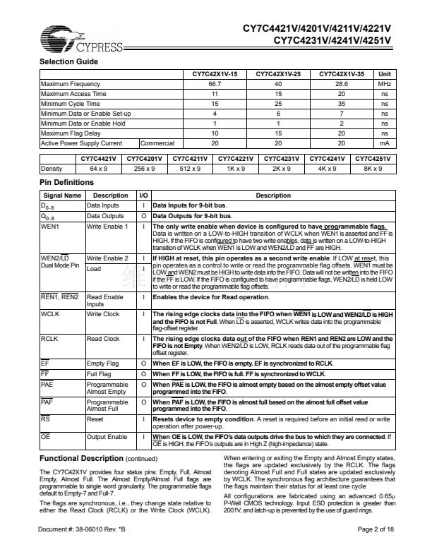
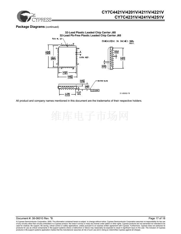
鈥?/div>
32-pin PLCC
鈥?Available in Pb-Free Packages
Functional Description
The CY7C42X1V are high-speed, low-power, FIFO memories
with clocked read and write interfaces. All are nine bits wide.
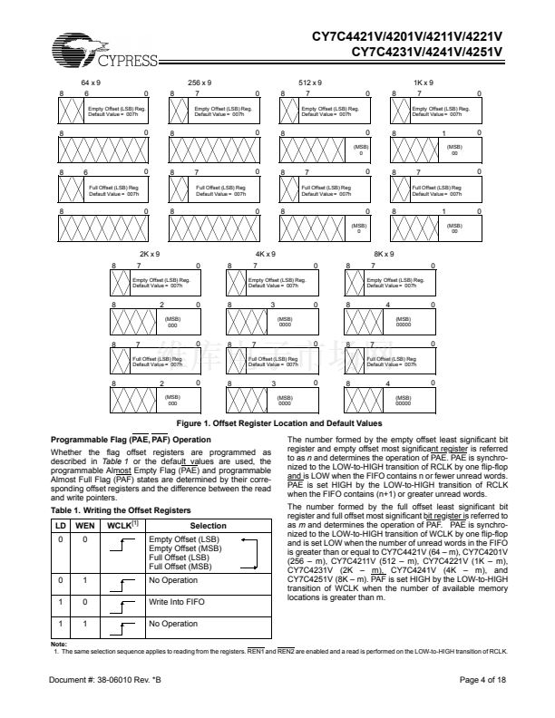
Programmable features include Almost Full/Almost Empty
flags. These FIFOs provide solutions for a wide variety of data
buffering needs, including high-speed data acquisition, multi-
processor interfaces, and communications buffering.
These FIFOs have 9-bit input and output ports that are
controlled by separate clock and enable signals. The input port
is controlled by a Free-Running Clock (WCLK) and two Write
Enable pins (WEN1, WEN2/LD).
When WEN1 is LOW and WEN2/LD is HIGH, data is written
into the FIFO on the rising edge of the WCLK signal. While
WEN1, WEN2/LD is held active, data is continually written into
the FIFO on each WCLK cycle. The output port is controlled in
a similar manner by a Free-Running Read Clock (RCLK) and
two Read Enable Pins (REN1, REN2). In addition, the
CY7C42X1V has an Output Enable Pin (OE). The Read
(RCLK) and Write (WCLK) clocks may be tied together for
single-clock operation or the two clocks may be run indepen-
dently for asynchronous read/write applications. Clock
frequencies up to 66 MHz are achievable.
Depth expansion is possible using one enable input for system
control, while the other enable is controlled by expansion logic
to direct the flow of data.
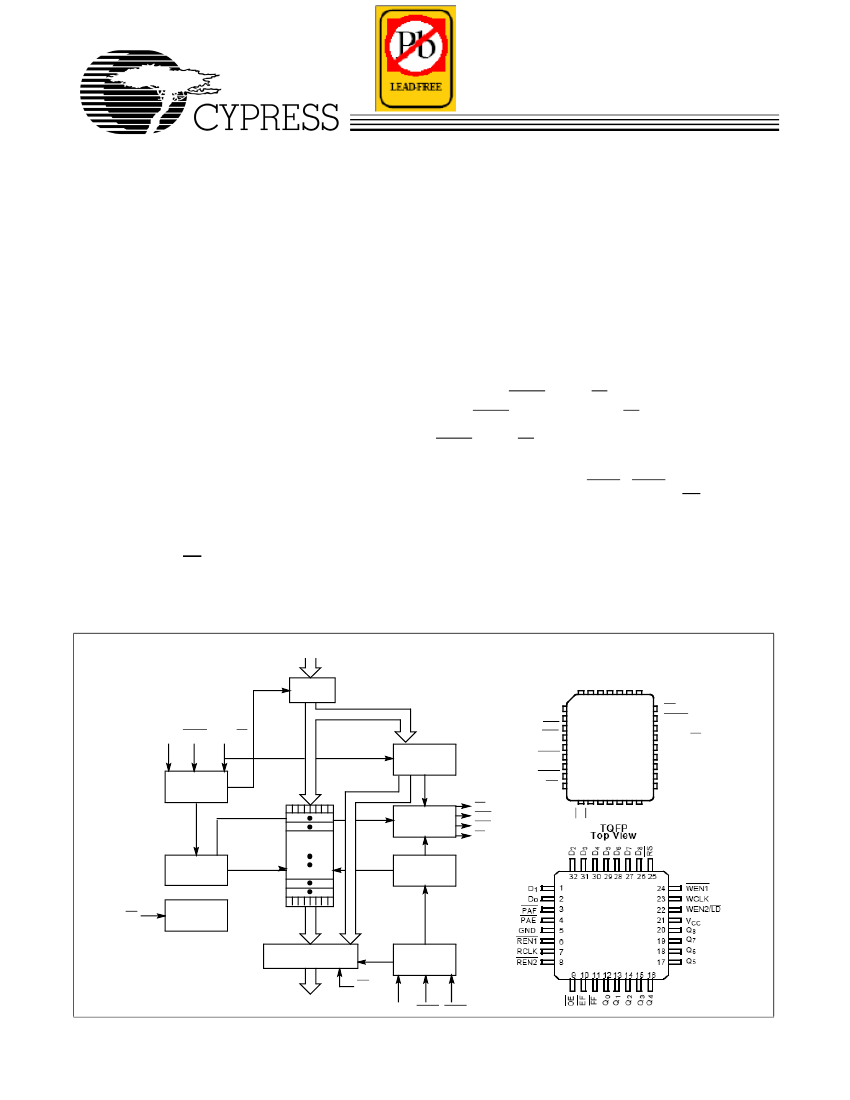
Logic Block Diagram
D0
鈭?/div>
8
Pin Configuration
PLCC
Top View
4 3 2 1 32 3130
29
5
28
6
27
7
26
8
9
25
10
24
11
23
22
12
21
13
14151617181920
EF
FF
Q
0
Q
1
Q
2
Q
3
Q
4
D
2
D
3
D
4
D
5
D
6
D
7
D
8
FLAG
PROGRAM
REGISTER
D
1
D
0
PAF
PAE
GND
REN1
RCLK
REN2
OE
EF
PAE
PAF
FF
RS
WEN1
WCLK
WEN2/LD
V
CC
Q
8
Q
7
Q
6
Q
5
FLAG
LOGIC
READ
POINTER
READ
CONTROL
OE
RCLK REN1 REN2
INPUT
REGISTER
WCLK WEN1 WEN2/LD
WRITE
CONTROL
Dual Port
RAM Array
64 x 9
WRITE
POINTER
8Kx 9
RS
RESET
LOGIC
THREE-ST
ATE
OUTPUTREGISTER
Q0
鈭?/div>
8
Cypress Semiconductor Corporation
Document #: 38-06010 Rev. *B
鈥?/div>
3901 North First Street
鈥?/div>
San Jose
,
CA 95134
鈥?/div>
408-943-2600
Revised July 14, 2005
CY7C4231V-25AXC PDF文件相关型号
CY7C4241V-15JXC,CY7C4251V-25AXC
CY7C4231V-25AXC 产品属性
250
集成电路 (IC)
逻辑 - FIFO
CY7C
同步
18K(2K x 9)
100MHz
15ns
3 V ~ 3.6 V
-40°C ~ 85°C
表面贴装
32-TQFP
32-TQFP(7x7)
管件
CY7C4231V-25AXC相关型号PDF文件下载
-
型号
版本
描述
厂商
下载
-
英文版
16K x 8/9 Dual-Port Static RAM with Sem, Int, Busy
Cypress
-
英文版
32K x 8/9 Dual-Port Static RAM
Cypress
-
英文版
64K/128K x 8/9 Dual-Port Static RAM
CYPRESS
-
英文版
64K/128K x 8/9 Dual-Port Static RAM
CYPRESS [C...
-
英文版
64K/128K x 8/9 Dual-Port Static RAM
CYPRESS
-
英文版
64K/128K x 8/9 Dual-Port Static RAM
CYPRESS [C...
-
英文版
4K x 16/18 and 8K x 16/18 Dual-Port Static RAM with SEM, INT...
CYPRESS
-
英文版
4K x 16/18 and 8K x 16/18 Dual-Port Static RAM with SEM, INT...
CYPRESS [C...
-
英文版
4K x 16/18 and 8K x 16/18 Dual-Port Static RAM with Sem, Int...
Cypress
-
英文版
16K x 16/18 Dual-Port Static RAM
Cypress
-
英文版
32K/64K x 16/18 Dual-Port Static RAM
CYPRESS
-
英文版
32K/64K x 16/18 Dual-Port Static RAM
CYPRESS [C...
-
英文版
32K/64K x 16/18 Dual-Port Static RAM
CYPRESS
-
英文版
32K/64K x 16/18 Dual-Port Static RAM
CYPRESS [C...


 1
1
 2
2
 3
3
 4
4
 5
5
 6
6
 7
7
 8
8
 9
9
 10
10
 11
11
 12
12
 13
13
 14
14
 15
15
 16
16
 17
17
 18
18
