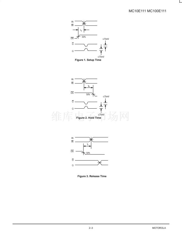
鈥?/div>
Low Skew
Guarateed Skew Spec
Differential Design
VBB Output
Enable
Extended 100E VEE Range of 鈥?.2 to 鈥?.46V
75k鈩?Input Pulldown Resistors
The device is specifically designed, modeled and produced with low
skew as the key goal. Optimal design and layout serve to minimize gate to
gate skew within-device, and empirical modeling is used to determine
process control limits that ensure consistent tpd distributions from lot to
lot. The net result is a dependable, guaranteed low skew device.
To ensure that the tight skew specification is met it is necessary that
both sides of the differential output are terminated into 50鈩? even if only
one side is being used. In most applications, all nine differential pairs will
be used and therefore terminated. In the case where fewer than nine
pairs are used, it is necessary to terminate at least the output pairs on the
same package side (i.e. sharing the same VCCO) as the pair(s) being
used on that side, in order to maintain minimum skew. Failure to do this
will result in small degradations of propagation delay (on the order of
10鈥?0ps) of the output(s) being used which, while not being catastrophic
to most designs, will mean a loss of skew margin.
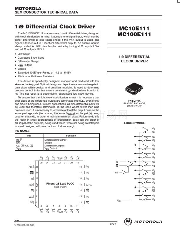
PIN NAMES
Pin
IN, IN
EN
Q0, Q0鈥換8, Q8
VBB
Function
Differential Input Pair
Enable
Differential Outputs
VBB Output
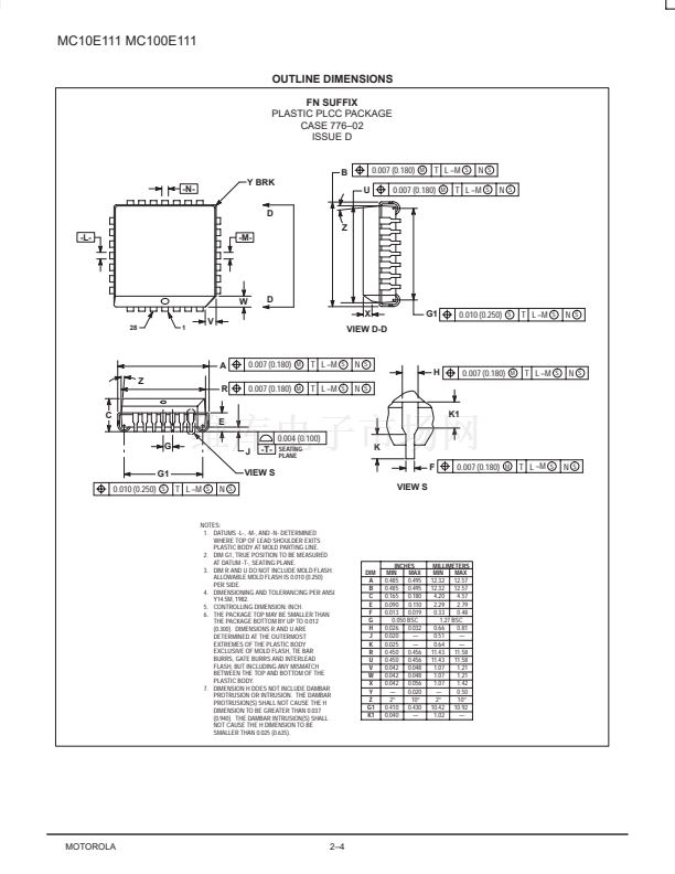
FN SUFFIX
PLASTIC PACKAGE
CASE 776-02
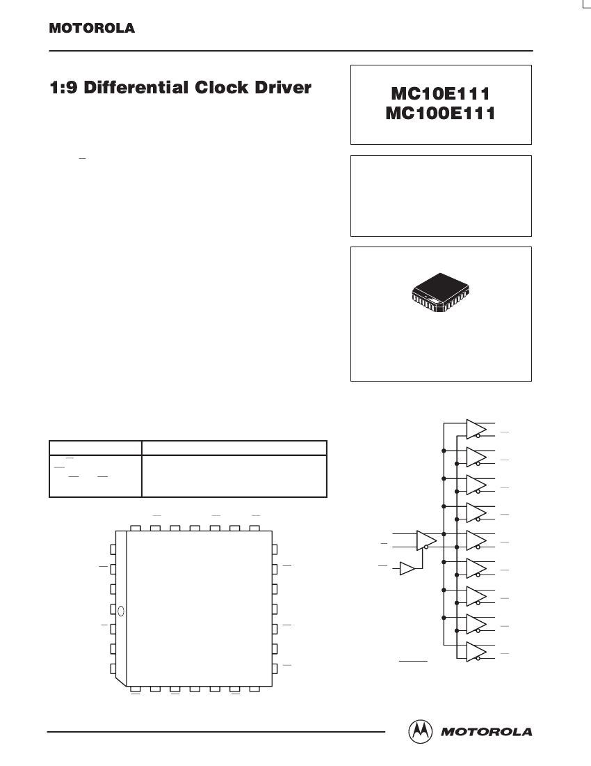
LOGIC SYMBOL
Q0
Q0
Q1
Q1
Q2
Q2
Q0
25
VEE
EN
IN
VCC
IN
VBB
NC
26
27
28
1
2
3
4
5
Q8
Q0
24
Q1 VCCO Q1
23
22
21
Q2
20
Q2
19
18
17
16
Q3
Q3
Q4
VCCO
Q4
Q5
Q5
VBB
IN
IN
EN
Q3
Q3
Q4
Q4
Q5
Q5
Q6
Q6
Q7
Q7
Q8
Q8
Pinout: 28-Lead PLCC
(Top View)
15
14
13
12
6
Q8
7
Q7
8
9
10
Q6
11
Q6
VCCO Q7
5/95
漏
Motorola, Inc. 1996
2鈥?
REV 3


 1
1
 2
2
 3
3
 4
4
 5
5
