SN54AHC367, SN74AHC367
HEX BUFFERS AND LINE DRIVERS
WITH 3-STATE OUTPUTS
SCLS424E 鈥?JUNE 1998 鈥?REVISED FEBRUARY 2002
D
D
D
Operating Range 2-V to 5.5-V V
CC
Latch-Up Performance Exceeds 100 mA Per
JESD 78, Class II
ESD Protection Exceeds JESD 22
鈥?2000-V Human-Body Model (A114-A)
鈥?200-V Machine Model (A115-A)
鈥?1000-V Charged-Device Model (C101)
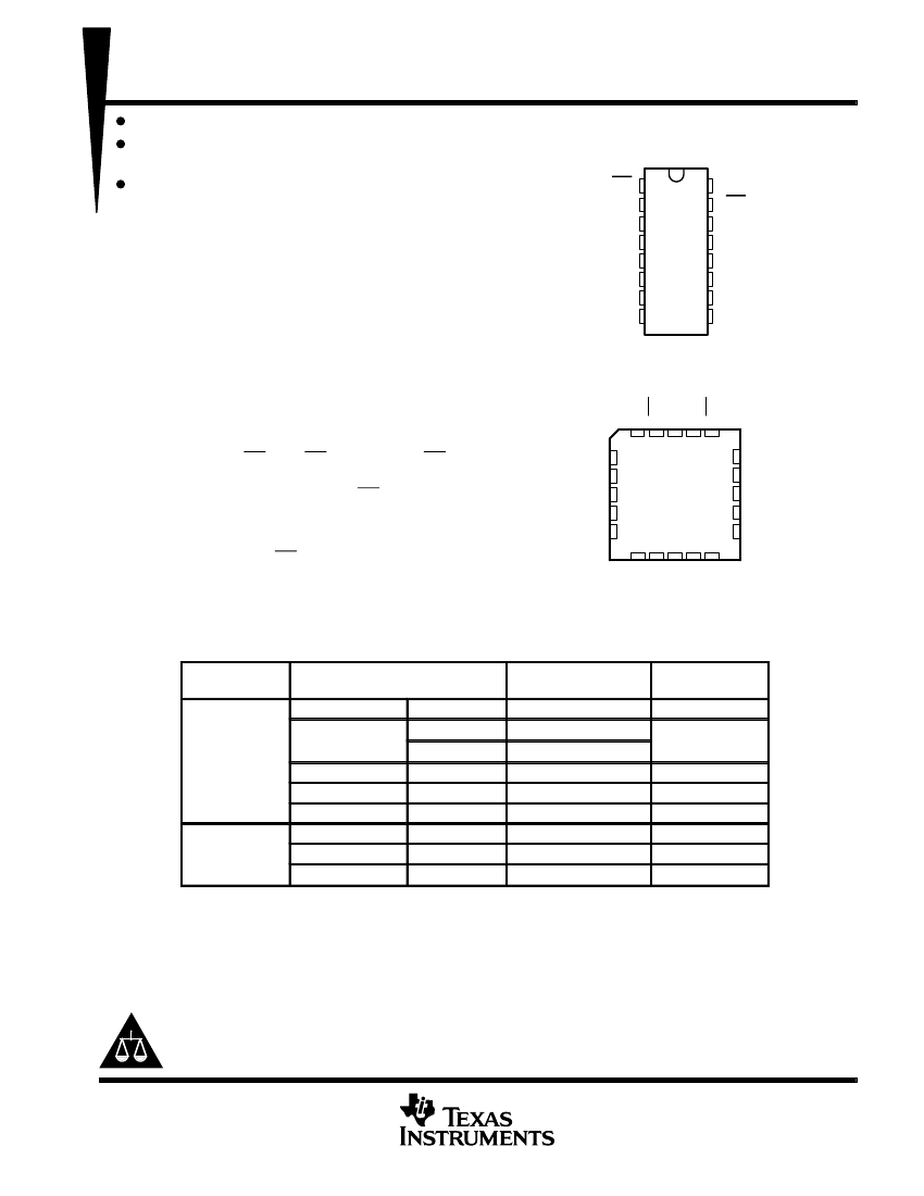
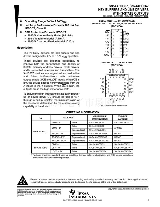
SN54AHC367 . . . J OR W PACKAGE
SN74AHC367 . . . D, DB, DGV, N, OR PW PACKAGE
(TOP VIEW)
description
The 鈥橝HC367 devices are hex buffers and line
drivers designed for 2-V to 5.5-V V
CC
operation.
These devices are designed specifically to
improve both the performance and density of
3-state memory address drivers, clock drivers,
and bus-oriented receivers and transmitters. The
鈥橝HC367 devices are organized as dual 4-line
and 2-line buffers/drivers with active-low
output-enable (1OE and 2OE) inputs. When OE is
low, the device passes noninverted data from the
A inputs to the Y outputs. When OE is high, the
outputs are in the high-impedance state.
To ensure the high-impedance state during power
up or power down, OE should be tied to V
CC
through a pullup resistor; the minimum value of
the resistor is determined by the current-sinking
capability of the driver.
ORDERING INFORMATION
TA
PDIP 鈥?N
SOIC 鈥?D
鈥?0掳C to 85掳C
SSOP 鈥?DB
TSSOP 鈥?PW
TVSOP 鈥?DGV
CDIP 鈥?J
鈥?5掳C to 125掳C
CFP 鈥?W
LCCC 鈥?FK
PACKAGE鈥?/div>
Tube
Tube
Tape and reel
Tape and reel
Tape and reel
Tape and reel
Tube
Tube
Tube
1OE
1A1
1Y1
1A2
1Y2
1A3
1Y3
GND
1
2
3
4
5
6
7
8
16
15
14
13
12
11
10
9
V
CC
2OE
2A2
2Y2
2A1
2Y1
1A4
1Y4
SN54AHC367 . . . FK PACKAGE
(TOP VIEW)
1A1
1OE
NC
V
CC
2OE
1Y1
1A2
NC
1Y2
1A3
4
5
6
7
8
3 2 1 20 19
18
17
16
15
14
9 10 11 12 13
2A2
2Y2
NC
2A1
2Y1
NC 鈥?No internal connection
ORDERABLE
PART NUMBER
SN74AHC367N
SN74AHC367D
SN74AHC367DR
SN74AHC367DBR
SN74AHC367PWR
SN74AHC367DGVR
SNJ54AHC367J
SNJ54AHC367W
SNJ54AHC367FK
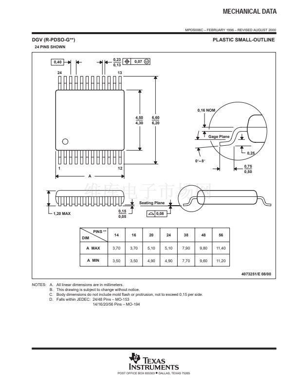
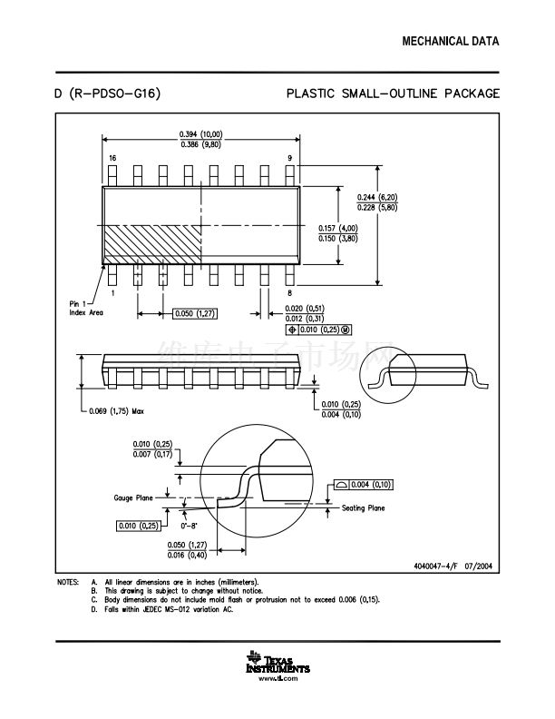
鈥?Package drawings, standard packing quantities, thermal data, symbolization, and PCB design guidelines
are available at www.ti.com/sc/package.
Please be aware that an important notice concerning availability, standard warranty, and use in critical applications of
Texas Instruments semiconductor products and disclaimers thereto appears at the end of this data sheet.
Copyright
铮?/div>
2002, Texas Instruments Incorporated
UNLESS OTHERWISE NOTED this document contains PRODUCTION
DATA information current as of publication date. Products conform to
specifications per the terms of Texas Instruments standard warranty.
Production processing does not necessarily include testing of all
parameters.
POST OFFICE BOX 655303
鈥?/div>
DALLAS, TEXAS 75265
1Y3
GND
NC
1Y4
1A4
TOP-SIDE
MARKING
SN74AHC367N
AHC367
HA367
HA367
HA367
SNJ54AHC367J
SNJ54AHC367W
SNJ54AHC367FK
1


 1
1
 2
2
 3
3
 4
4
 5
5
 6
6
 7
7
 8
8
 9
9
 10
10
 11
11
 12
12
