CY7C4421V/4201V/4211V/4221V
CY7C4231V/4241V/4251V
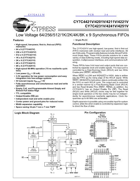
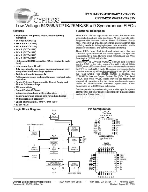
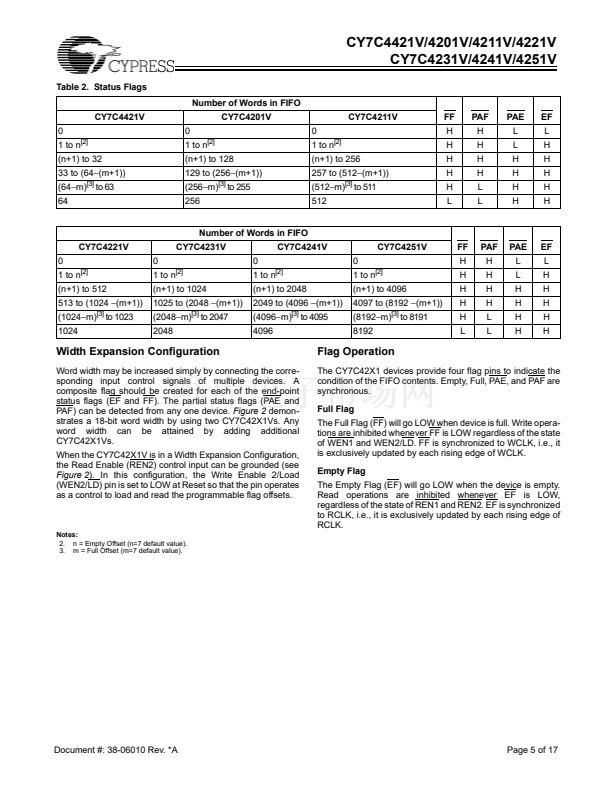
Architecture
The CY7C42X1V consists of an array of 64 to 8K words of nine
bits each (implemented by a dual-port array of SRAM cells),
a read pointer, a write pointer, control signals (RCLK, WCLK,
REN1, REN2, WEN1, WEN2, RS), and flags (EF, PAE, PAF,
FF.)
Write Enable 2/Load (WEN2/LD).
This is a dual-purpose pin.
The FIFO is configured at Reset to have programmable flags
or to have two write enables, which allows for depth
expansion. If Write Enable 2/Load (WEN2/LD) is set active
HIGH at Reset (RS=LOW), this pin operates as a second write
enable pin.
If the FIFO is configured to have two write enables, when Write
Enable (WEN1) is LOW and Write Enable 2/Load (WEN2/LD)
is HIGH, data can be loaded into the input register and RAM
array on the LOW-to-HIGH transition of every write clock
(WCLK.) Data is stored in the RAM array sequentially and
independently of any on-going read operation.
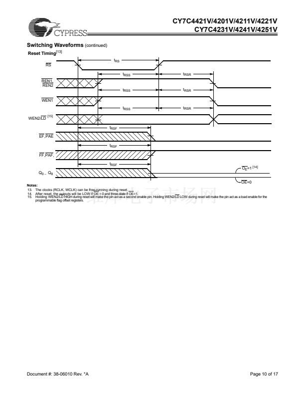
Resetting the FIFO
Upon power-up, the FIFO must be reset with a Reset (RS)
cycle. This causes the FIFO to enter the Empty condition
signified by EF being LOW. All data outputs (Q
0-8
) go LOW
t
RSF
after the rising edge of RS. In order for the FIFO to reset
to its default state, a falling edge must occur on RS and the
user must not read or write while RS is LOW. All flags are
guaranteed to be valid t
RSF
after RS is taken LOW.
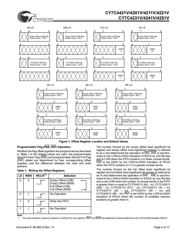
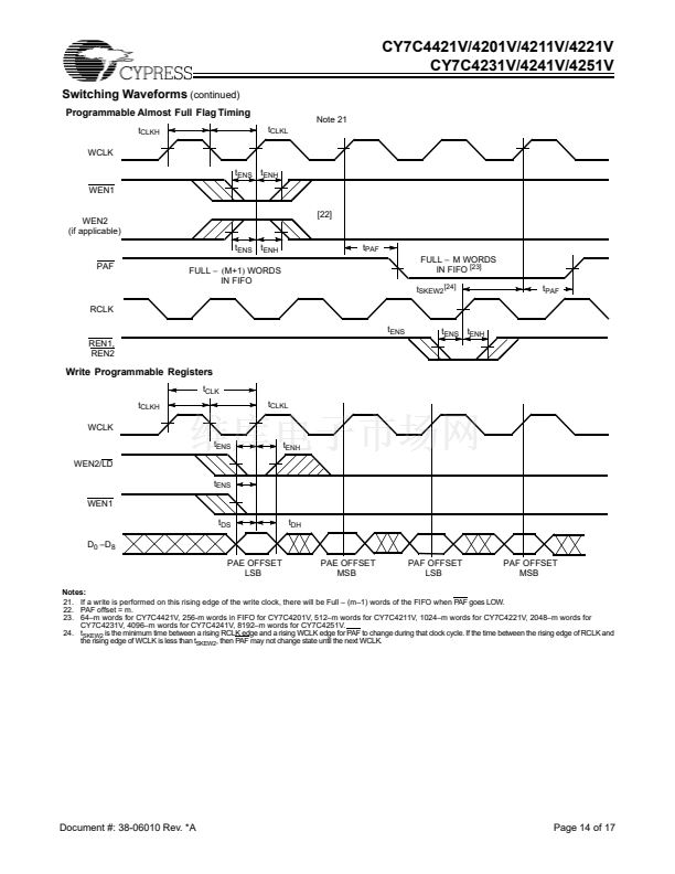
Programming
When WEN2/LD is held LOW during Reset, this pin is the load
(LD) enable for flag offset programming. In this configuration,
WEN2/LD can be used to access the four 8-bit offset registers
contained in the CY7C42X1V for writing or reading data to
these registers.
When the device is configured for programmable flags and
both WEN2/LD and WEN1 are LOW, the first LOW-to-HIGH
transition of WCLK writes data from the data inputs to the
empty offset Least Significant Bit (LSB) register. The second,
third, and fourth LOW-to-HIGH transitions of WCLK store data
in the empty offset Most Significant Bit (MSB) register, full
offset LSB register, and full offset MSB register, respectively,
when WEN2/LD and WEN1 are LOW. The fifth LOW-to-HIGH
transition of WCLK while WEN2/LD and WEN1 are LOW
writes data to the empty LSB register again.
Figure 1
shows
the register sizes and default values for the various device
types.
It is not necessary to write to all the offset registers at one time.
A subset of the offset registers can be written; then by bringing
the WEN2/LD input HIGH, the FIFO is returned to normal read
and write operation. The next time WEN2/LD is brought LOW,
a write operation stores data in the next offset register in
sequence.
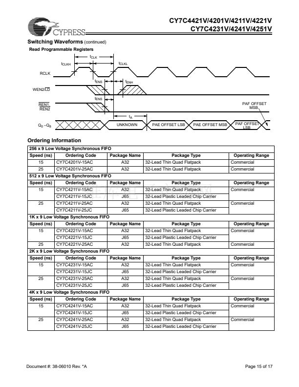
The contents of the offset registers can be read to the data
outputs when WEN2/LD is LOW and both REN1 and REN2
are LOW. LOW-to-HIGH transitions of RCLK read register
contents to the data outputs. Writes and reads should not be
performed simultaneously on the offset registers.
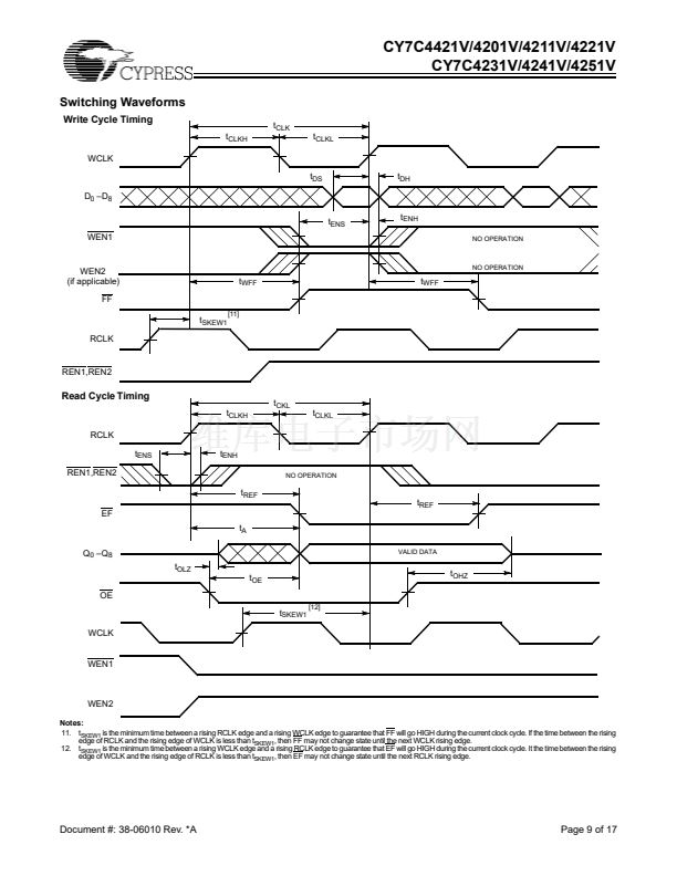
FIFO Operation
When the WEN1 signal is active LOW and WEN2 is active HIGH,
data present on the D
0-8
pins is written into the FIFO on each
rising edge of the WCLK signal. Similarly, when the REN1 and
REN2 signals are active LOW, data in the FIFO memory will
be presented on the Q
0-8
outputs. New data will be presented
on each rising edge of RCLK while REN1 and REN2 are
active. REN1 and REN2 must set up t
ENS
before RCLK for it
to be a valid read function. WEN1 and WEN2 must occur t
ENS
before WCLK for it to be a valid write function.
An Output Enable (OE) pin is provided to three-state the Q
0-8
outputs when OE is asserted. When OE is enabled (LOW), data
in the output register will be available to the Q
0-8
outputs after t
OE
.
The FIFO contains overflow circuitry to disallow additional
writes when the FIFO is full, and underflow circuitry to disallow
additional reads when the FIFO is empty. An empty FIFO
maintains the data of the last valid read on its Q
0-8
outputs
even after additional reads occur.
Write Enable 1 (WEN1).
If the FIFO is configured for program-
mable flags, Write Enable 1 (WEN1) is the only write enable
control pin. In this configuration, when Write Enable 1 (WEN1)
is LOW, data can be loaded into the input register and RAM
array on the LOW-to-HIGH transition of every write clock
(WCLK). Data is stored is the RAM array sequentially and
independently of any on-going read operation.
Document #: 38-06010 Rev. *A
Page 3 of 17


 1
1
 2
2
 3
3
 4
4
 5
5
 6
6
 7
7
 8
8
 9
9
 10
10
 11
11
 12
12
 13
13
 14
14
 15
15
 16
16
 17
17
