CY7C4421V/4201V/4211V/4221V
CY7C4231V/4241V/4251V
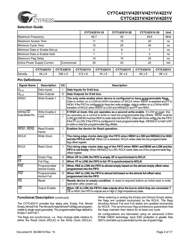
Selection Guide
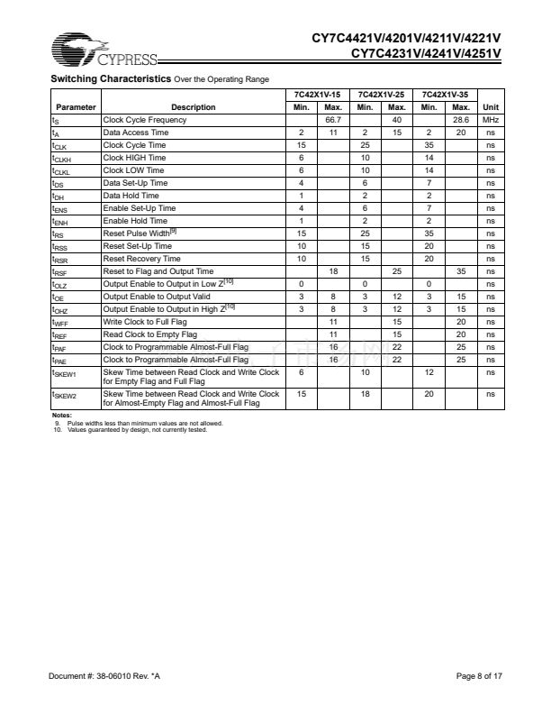
CY7C42X1V-15
Maximum Frequency
Maximum Access Time
Minimum Cycle Time
Minimum Data or Enable Set-up
Minimum Data or Enable Hold
Maximum Flag Delay
Active Power Supply Current
CY7C4421V
Density
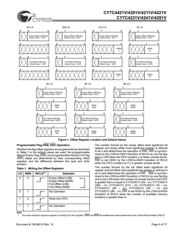
64 x 9
Commercial
CY7C4201V
256 x 9
CY7C4211V
512 x 9
66.7
11
15
4
1
10
20
CY7C4221V
1K x 9
CY7C42X1V-25
40
15
25
6
1
15
20
CY7C4231V
2K x 9
CY7C42X1V-35
28.6
20
35
7
2
20
20
CY7C4241V
4K x 9
Unit
MHz
ns
ns
ns
ns
ns
mA
CY7C4251V
8K x 9
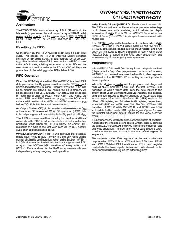
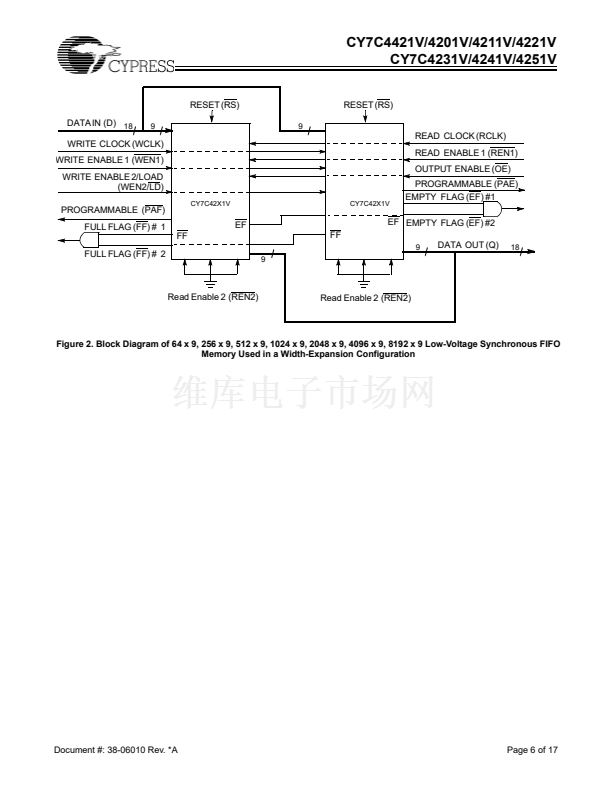
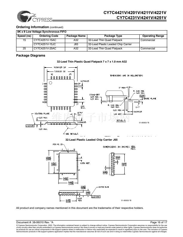
Pin Definitions
Signal Name
D
0鈭?
Q
0鈭?
WEN1
Description
Data Inputs
Data Outputs
Write Enable 1
I/O
I
O
I
Data Inputs for 9-bit bus.
Data Outputs for 9-bit bus.
The only write enable when device is configured to have programmable flags.
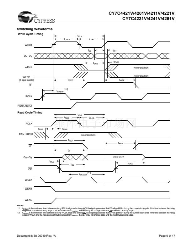
Data is written on a LOW-to-HIGH transition of WCLK when WEN1 is asserted and FF is
HIGH. If the FIFO is configured to have two write enables, data is written on a LOW-to-HIGH
transition of WCLK when WEN1 is LOW and WEN2/LD and FF are HIGH.
If HIGH at reset, this pin operates as a second write enable.
If LOW at reset, this
pin operates as a control to write or read the programmable flag offsets. WEN1 must be
LOW and WEN2 must be HIGH to write data into the FIFO. Data will not be written into the FIFO
if the FF is LOW. If the FIFO is configured to have programmable flags, WEN2/LD is held LOW
to write or read the programmable flag offsets.
Enables the device for Read operation.
The rising edge clocks data into the FIFO when WEN1 is LOW and WEN2/LD is HIGH
and the FIFO is not Full.
When LD is asserted, WCLK writes data into the programmable
flag-offset register.
The rising edge clocks data out of the FIFO when REN1 and REN2 are LOW and the
FIFO is not Empty.
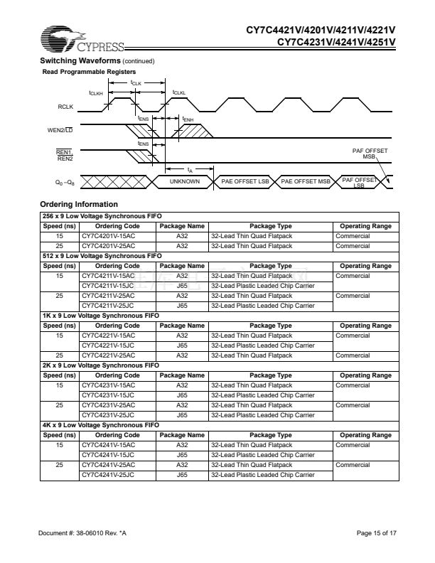
When WEN2/LD is LOW, RCLK reads data out of the programmable flag
offset register.
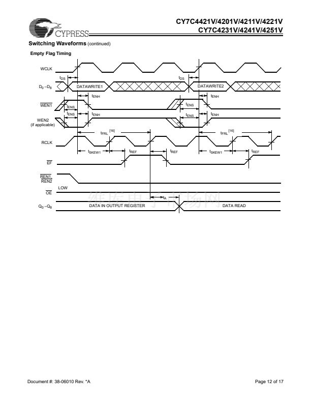
When EF is LOW, the FIFO is empty. EF is synchronized to RCLK.
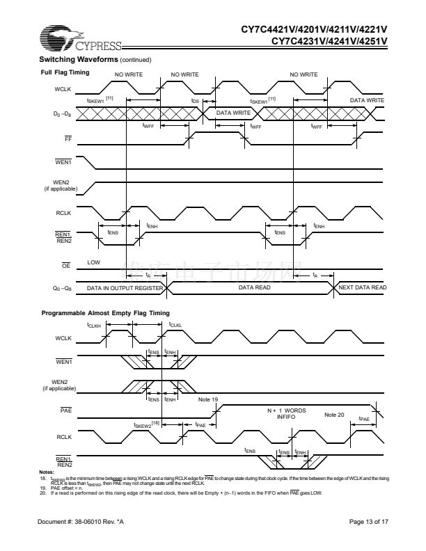
When FF is LOW, the FIFO is full. FF is synchronized to WCLK.
When PAE is LOW, the FIFO is almost empty based on the almost empty offset value
programmed into the FIFO.
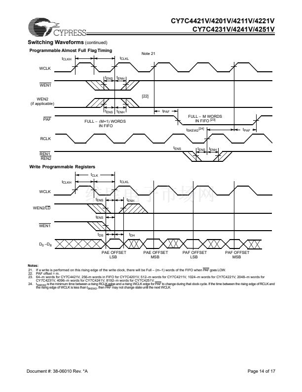
When PAF is LOW, the FIFO is almost full based on the almost full offset value
programmed into the FIFO.
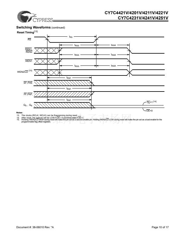
Resets device to empty condition.
A reset is required before an initial read or write
operation after power-up.
When OE is LOW, the FIFO鈥檚 data outputs drive the bus to which they are connected.
If
OE is HIGH, the FIFO鈥檚 outputs are in High Z (high-impedance) state.
When entering or exiting the Empty and Almost Empty states,
the flags are updated exclusively by the RCLK. The flags
denoting Almost Full and Full states are updated exclusively
by WCLK. The synchronous flag architecture guarantees that
the flags maintain their status for at least one cycle
All configurations are fabricated using an advanced 0.65m
P-Well CMOS technology. Input ESD protection is greater than
2001V, and latch-up is prevented by the use of guard rings.
Description
WEN2/LD
Dual Mode Pin
Write Enable 2
Load
I
I
REN1, REN2
WCLK
Read Enable
Inputs
Write Clock
I
I
RCLK
Read Clock
I
EF
FF
PAE
PAF
RS
OE
Empty Flag
Full Flag
Programmable
Almost Empty
Programmable
Almost Full
Reset
Output Enable
O
O
O
O
I
I
Functional Description
(continued)
The CY7C42X1V provides four status pins: Empty, Full, Almost
Empty, Almost Full. The Almost Empty/Almost Full flags are program-
mable to single word granularity. The programmable flags default to
Empty-7 and Full-7.
The flags are synchronous, i.e., they change state relative to
either the Read Clock (RCLK) or the Write Clock (WCLK).
Document #: 38-06010 Rev. *A
Page 2 of 17


 1
1
 2
2
 3
3
 4
4
 5
5
 6
6
 7
7
 8
8
 9
9
 10
10
 11
11
 12
12
 13
13
 14
14
 15
15
 16
16
 17
17
