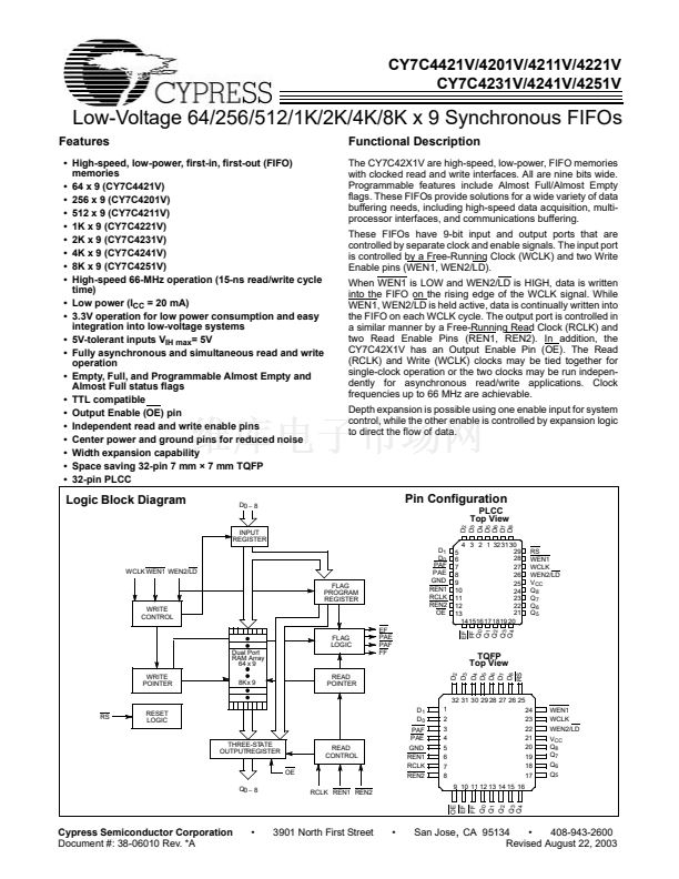
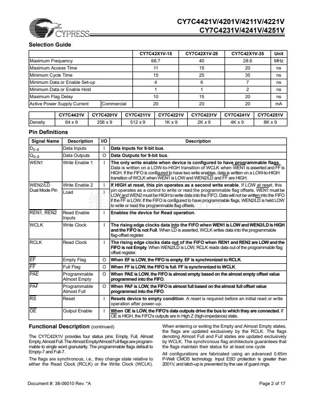
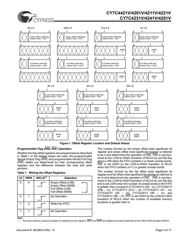
CY7C4421V/4201V/4211V/4221V
CY7C4231V/4241V/4251V
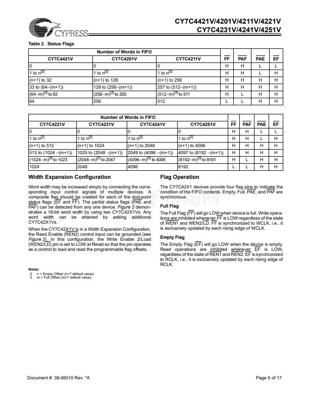
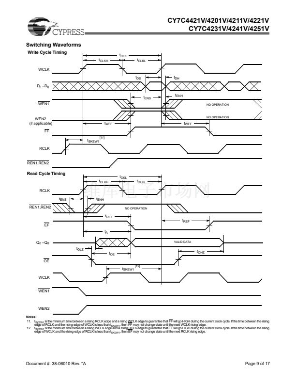
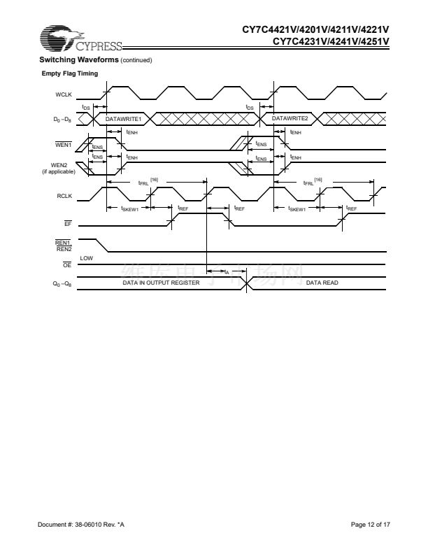
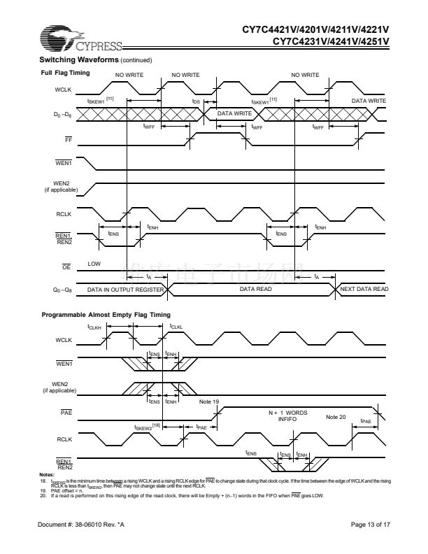
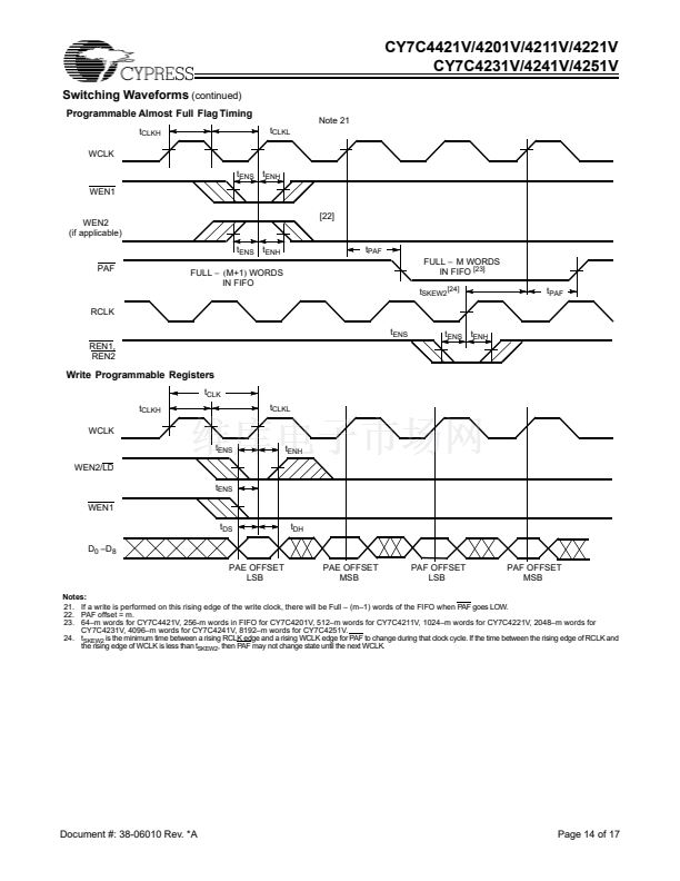
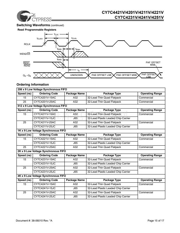
Switching Waveforms
Write Cycle Timing
t
CLKH
WCLK
t
DS
D
0
鈥揇
8
t
ENS
WEN1
t
ENH
NO OPERATION
t
CLK
t
CLKL
t
DH
WEN2
(if applicable)
FF
t
SKEW1
RCLK
[11]
NO OPERATION
t
WFF
t
WFF
REN1,REN2
Read Cycle Timing
t
CLKH
RCLK
t
ENS
REN1,REN2
t
REF
EF
t
A
Q
0
鈥換
8
t
OLZ
t
OE
OE
t
ENH
t
CKL
t
CLKL
NO OPERATION
t
REF
VALID DATA
t
OHZ
t
SKEW1
WCLK
[12]
WEN1
WEN2
Notes:
11. t
SKEW1
is the minimum time between a rising RCLK edge and a rising WCLK edge to guarantee that FF will go HIGH during the current clock cycle. If the time between the rising
edge of RCLK and the rising edge of WCLK is less than t
SKEW1
, then FF may not change state until the next WCLK rising edge.
12. t
SKEW1
is the minimum time between a rising WCLK edge and a rising RCLK edge to guarantee that EF will go HIGH during the current clock cycle. It the time between the rising
edge of WCLK and the rising edge of RCLK is less than t
SKEW1
, then EF may not change state until the next RCLK rising edge.
Document #: 38-06010 Rev. *A
Page 9 of 17


 1
1
 2
2
 3
3
 4
4
 5
5
 6
6
 7
7
 8
8
 9
9
 10
10
 11
11
 12
12
 13
13
 14
14
 15
15
 16
16
 17
17
