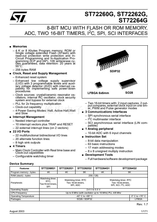
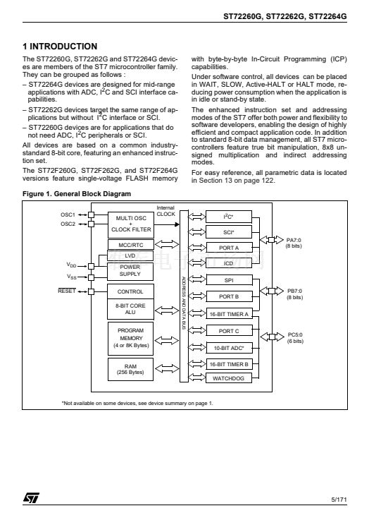
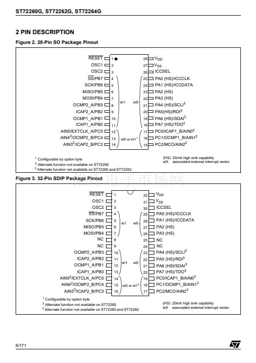
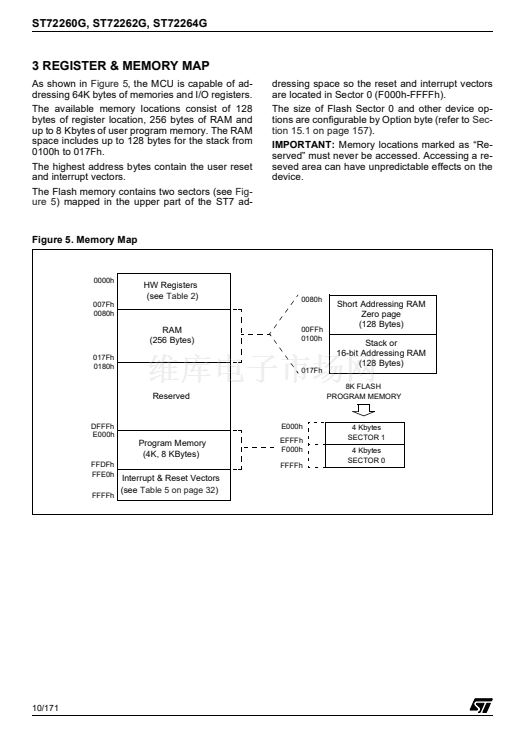
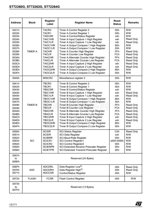
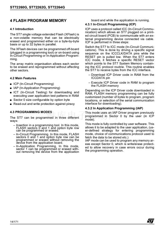
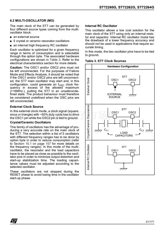
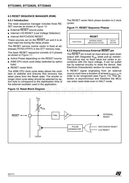
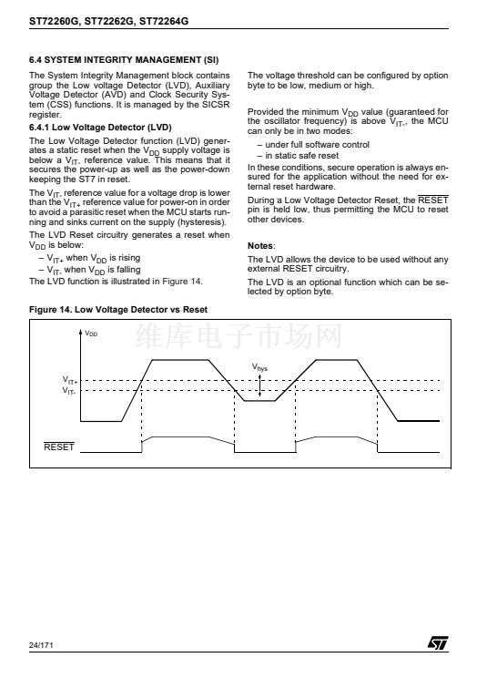
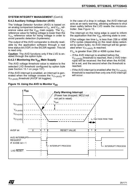
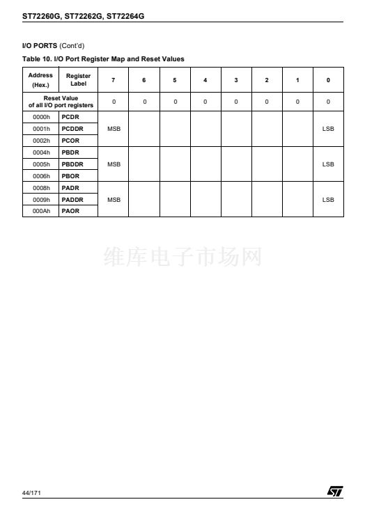
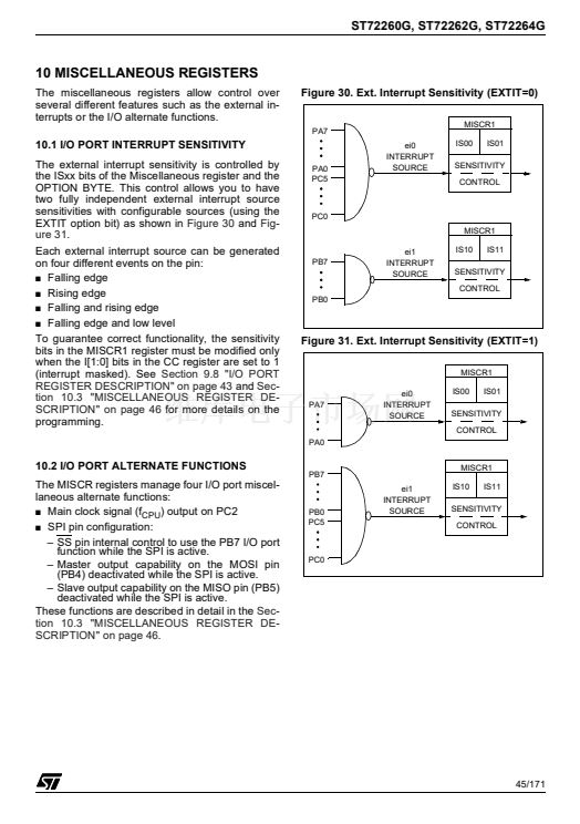
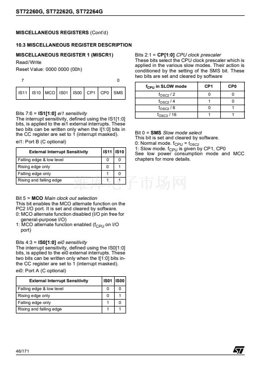
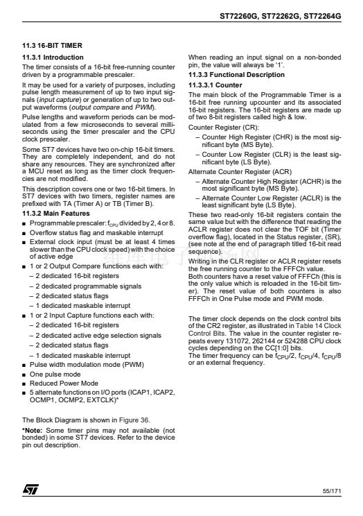
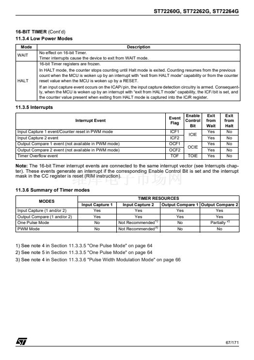
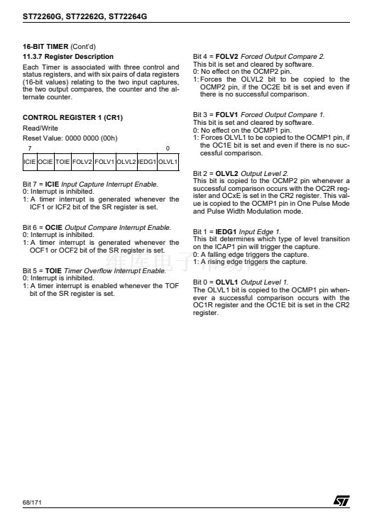
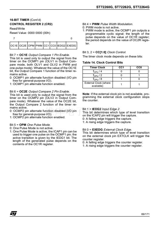
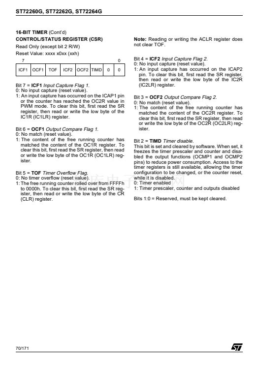
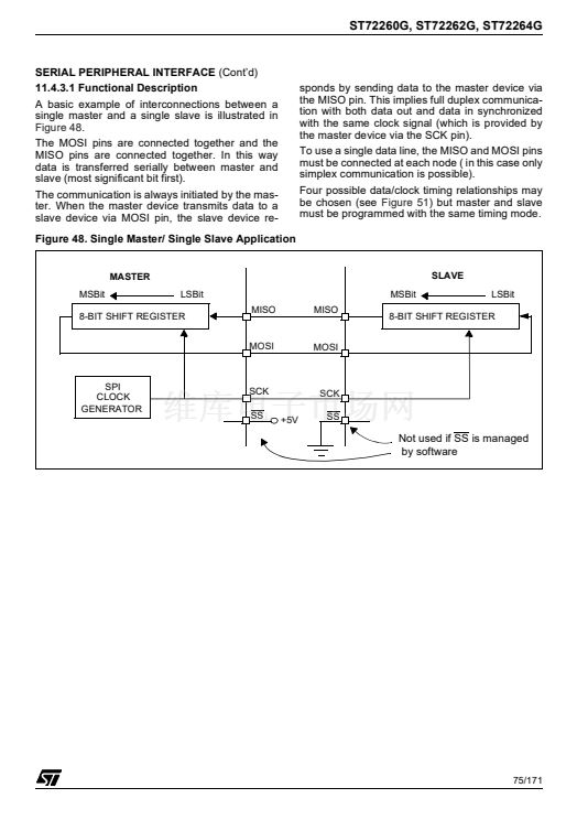
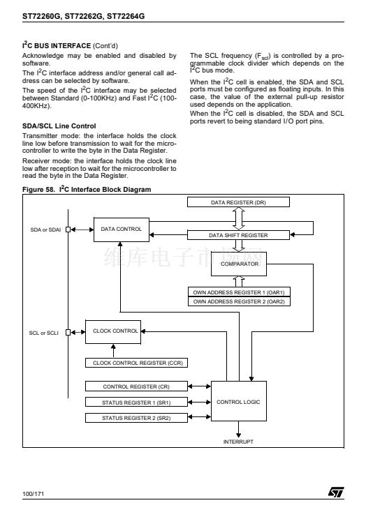
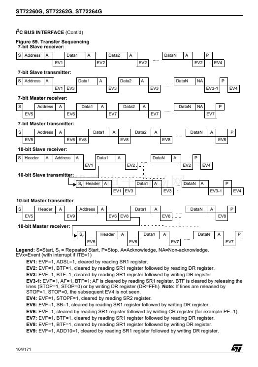
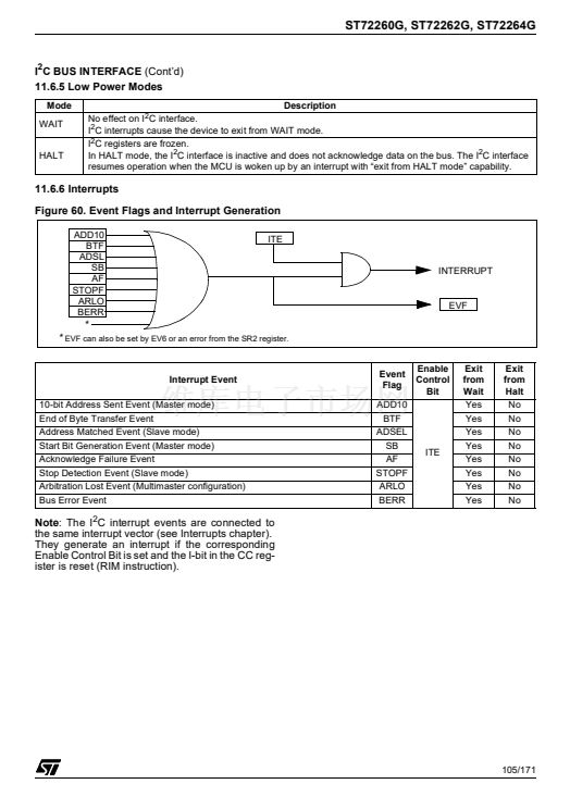
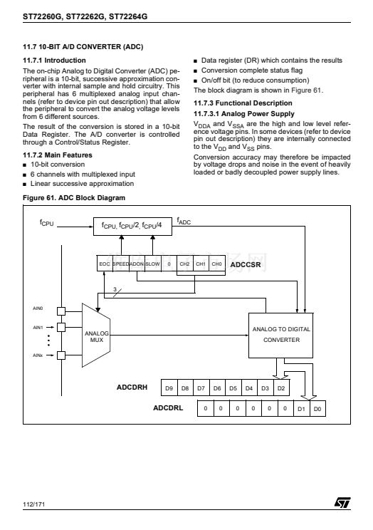
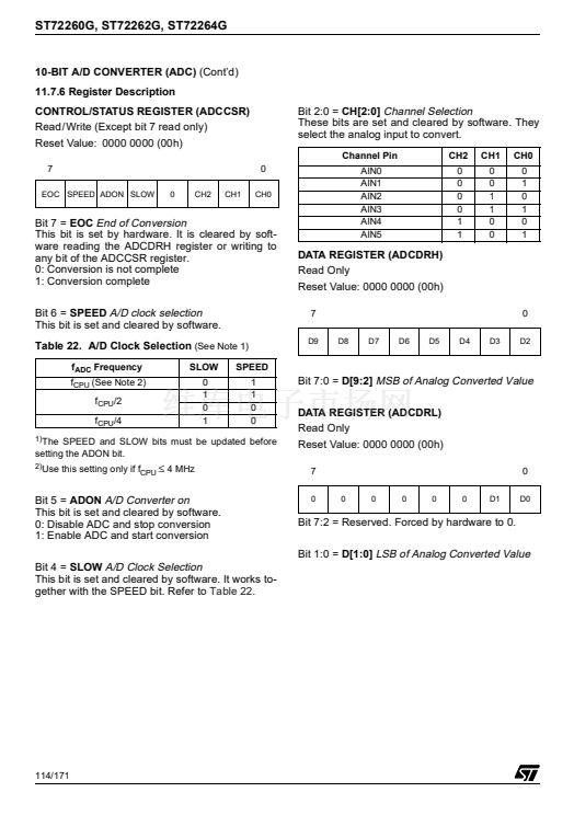
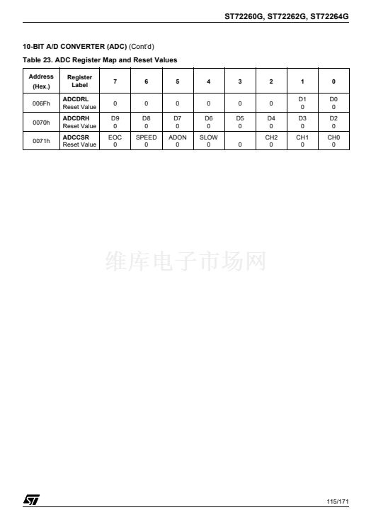
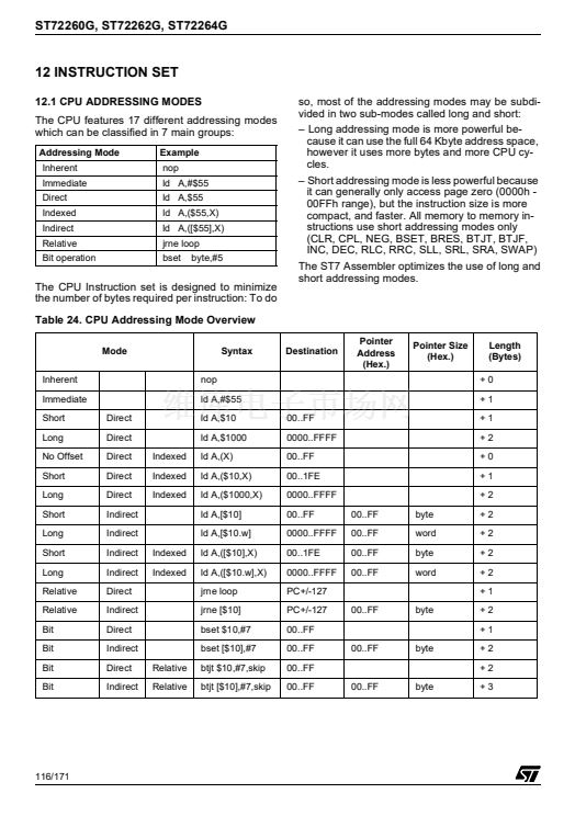
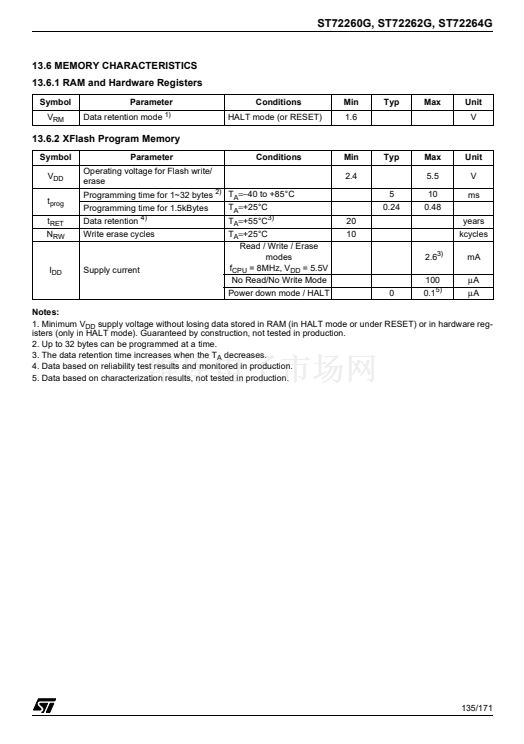
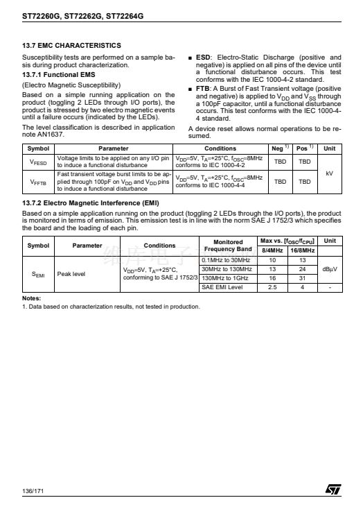
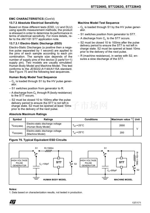
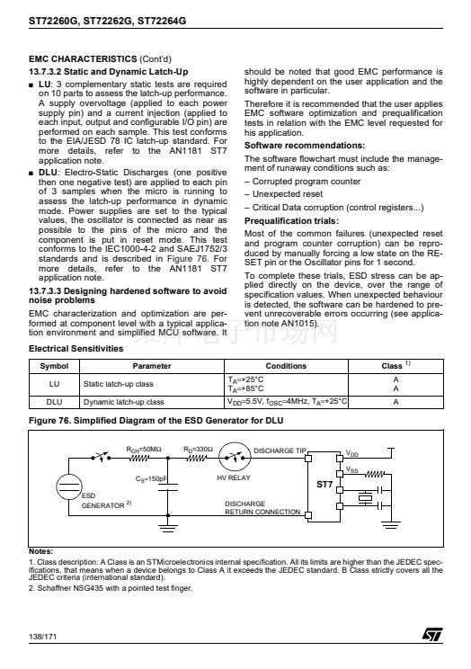
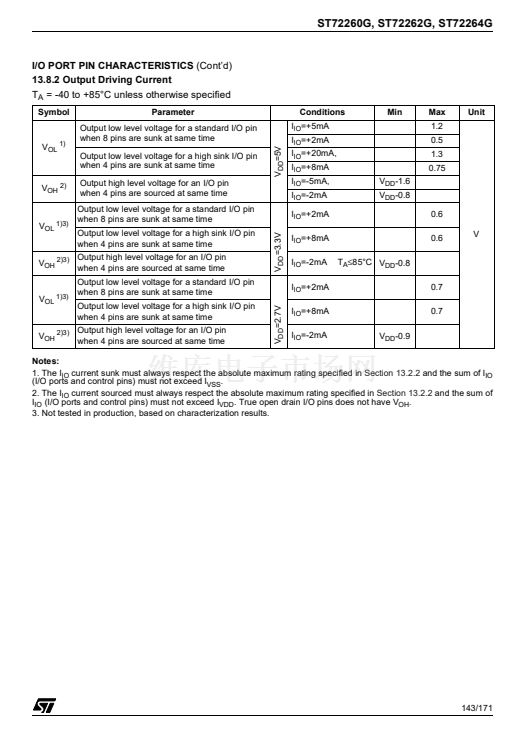
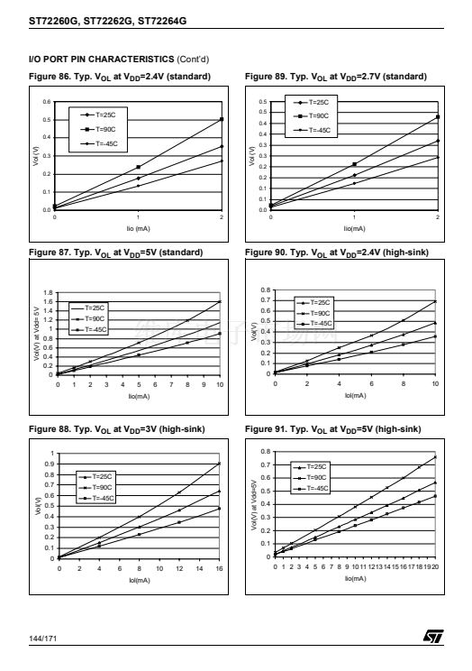
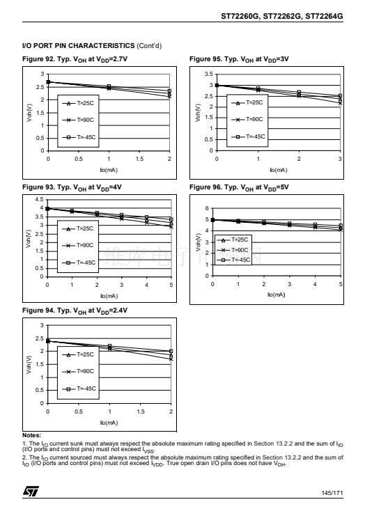
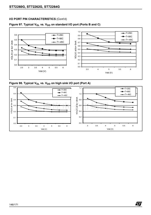
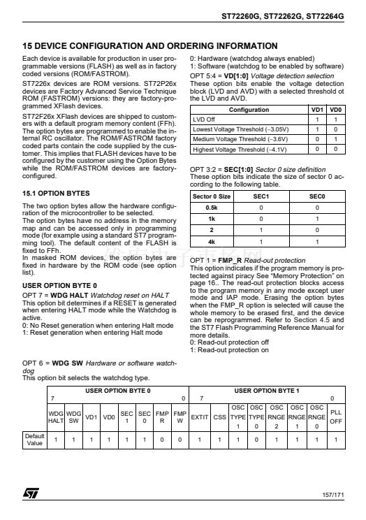
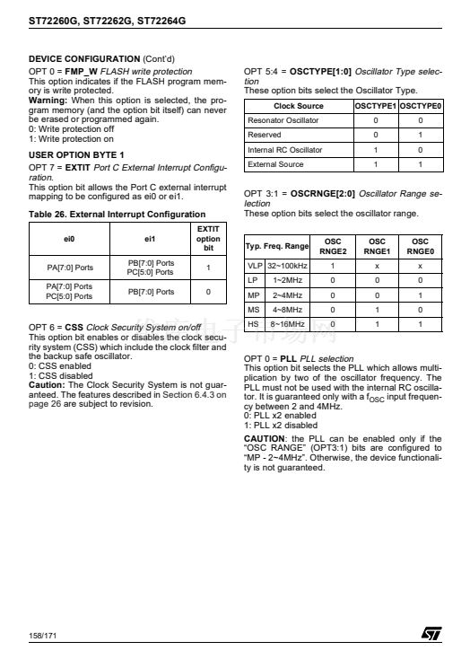
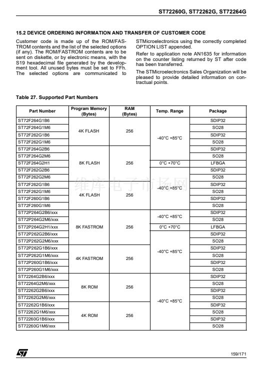
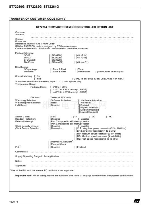
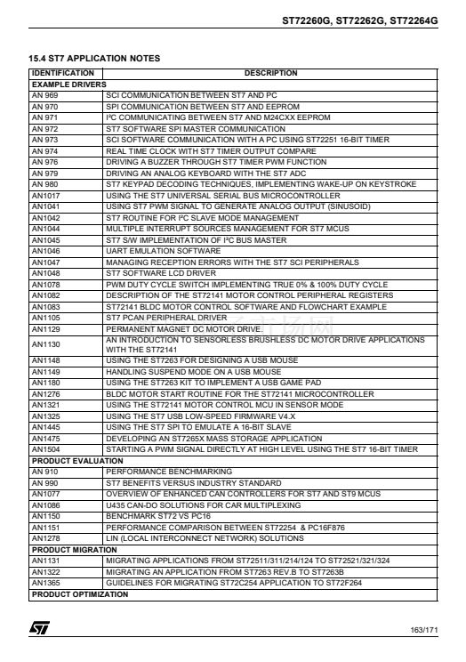
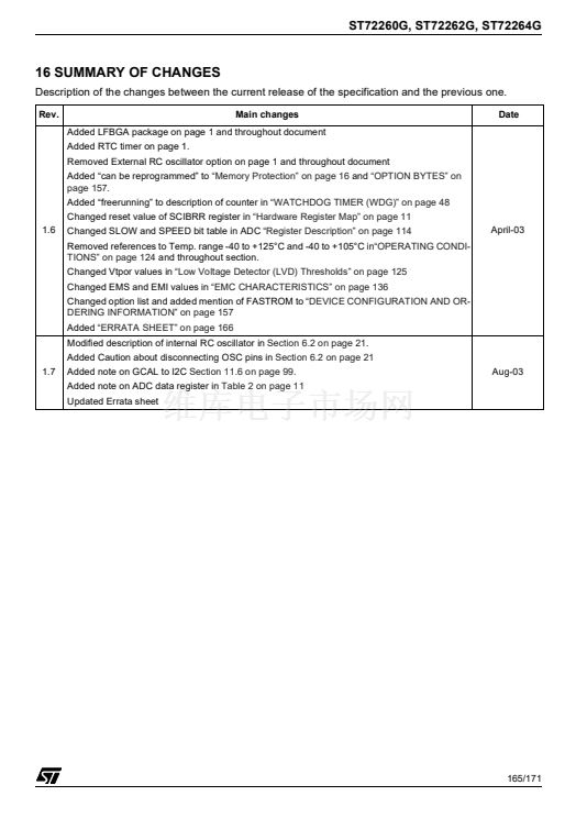
ST72260G, ST72262G, ST72264G
MISCELLANEOUS REGISTERS
(Cont鈥檇)
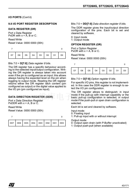
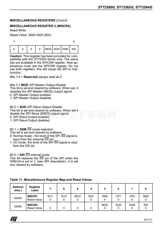
MISCELLANEOUS REGISTER 2 (MISCR2)
Read /Write
Reset Value: 0000 0000 (00h)
7
0
0
0
0
MOD SOD
SSM
0
SSI
Caution:
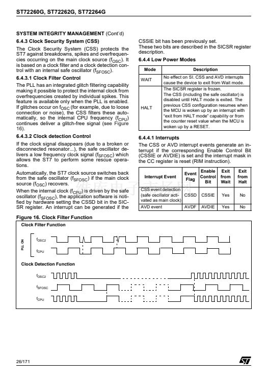
This register has been provided for com-
patibility with the ST72254 family only. The same
bits are available in the SPICSR register. New ap-
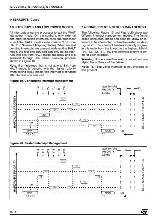
plications must use the SPICSR register. Do not
use both registers, this will cause the SPI to mal-
function.
Bits 7:4 =
Reserved
always read as 0
Bits 3 =
MOD
SPI Master Output Disable
This bit is set and cleared by software. When set, it
disables the SPI Master (MOSI) output signal.
0: SPI Master Output enabled.
1: SPI Master Output disabled.
Bit 2 =
SOD
SPI Slave Output Disable
This bit is set and cleared by software. When set it
disable the SPI Slave (MISO) output signal.
0: SPI Slave Output enabled.
1: SPI Slave Output disabled.
Bit 1 =
SSM
SS mode selection
This bit is set and cleared by software.
0: Normal mode - the level of the SPI SS signal is
input from the external SS pin.
1: I/O mode, the level of the SPI SS signal is read
from the SSI bit.
Bit 0 =
SSI
SS internal mode
This bit replaces the SS pin of the SPI when the
SSM bit is set to 1. (see SPI description). It is set
and cleared by software.
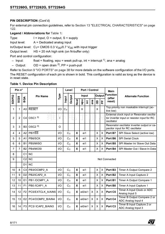
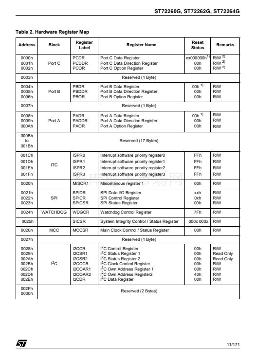
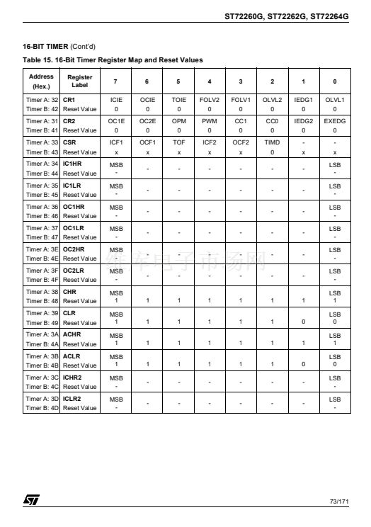
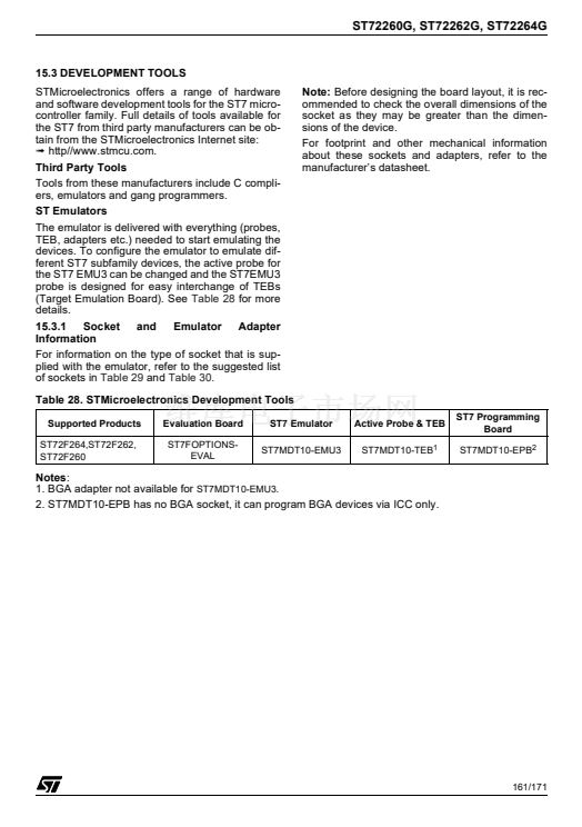
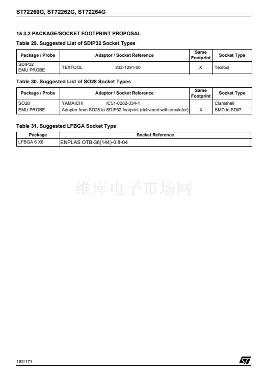
Table 11. Miscellaneous Register Map and Reset Values
Address
(Hex.)
0020h
0040h
Register
Label
MISCR1
Reset Value
MISCR2
Reset Value
7
IS11
0
0
6
IS10
0
0
5
MCO
0
0
4
IS01
0
0
3
IS00
0
MOD
0
2
CP1
0
SOD
0
1
CP0
0
SSM
0
0
SMS
0
SSI
0
47/171


 1
1
 2
2
 3
3
 4
4
 5
5
 6
6
 7
7
 8
8
 9
9
 10
10
 11
11
 12
12
 13
13
 14
14
 15
15
 16
16
 17
17
 18
18
 19
19
 20
20
 21
21
 22
22
 23
23
 24
24
 25
25
 26
26
 27
27
 28
28
 29
29
 30
30
 31
31
 32
32
 33
33
 34
34
 35
35
 36
36
 37
37
 38
38
 39
39
 40
40
 41
41
 42
42
 43
43
 44
44
 45
45
 46
46
 47
47
 48
48
 49
49
 50
50
 51
51
 52
52
 53
53
 54
54
 55
55
 56
56
 57
57
 58
58
 59
59
 60
60
 61
61
 62
62
 63
63
 64
64
 65
65
 66
66
 67
67
 68
68
 69
69
 70
70
 71
71
 72
72
 73
73
 74
74
 75
75
 76
76
 77
77
 78
78
 79
79
 80
80
 81
81
 82
82
 83
83
 84
84
 85
85
 86
86
 87
87
 88
88
 89
89
 90
90
 91
91
 92
92
 93
93
 94
94
 95
95
 96
96
 97
97
 98
98
 99
99
 100
100
 101
101
 102
102
 103
103
 104
104
 105
105
 106
106
 107
107
 108
108
 109
109
 110
110
 111
111
 112
112
 113
113
 114
114
 115
115
 116
116
 117
117
 118
118
 119
119
 120
120
 121
121
 122
122
 123
123
 124
124
 125
125
 126
126
 127
127
 128
128
 129
129
 130
130
 131
131
 132
132
 133
133
 134
134
 135
135
 136
136
 137
137
 138
138
 139
139
 140
140
 141
141
 142
142
 143
143
 144
144
 145
145
 146
146
 147
147
 148
148
 149
149
 150
150
 151
151
 152
152
 153
153
 154
154
 155
155
 156
156
 157
157
 158
158
 159
159
 160
160
 161
161
 162
162
 163
163
 164
164
 165
165
 166
166
 167
167
 168
168
 169
169
 170
170
 171
171
