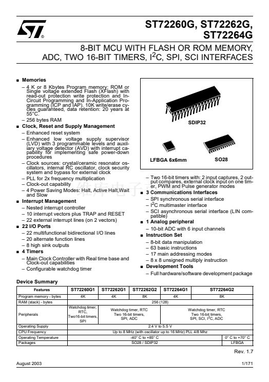
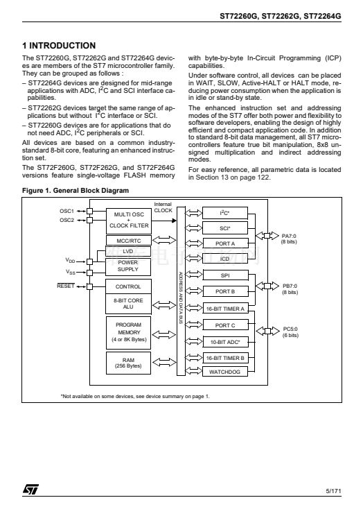
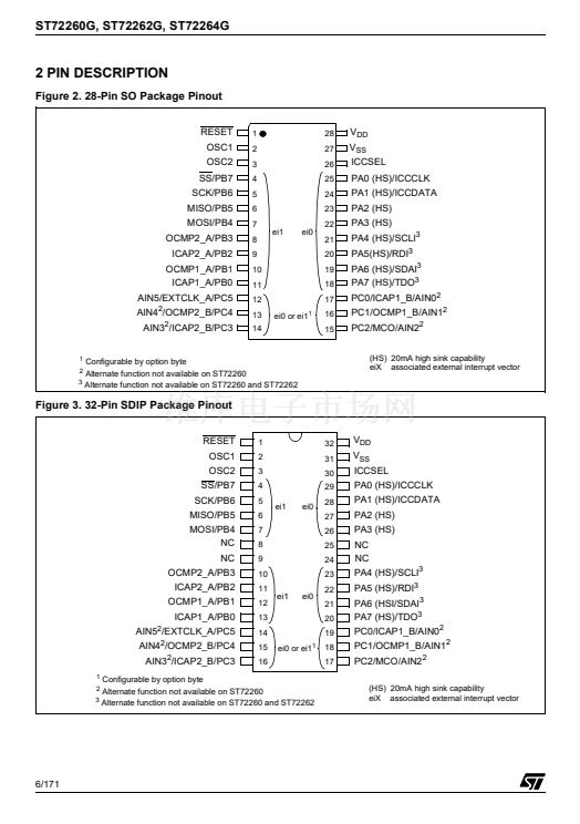
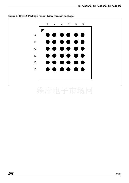
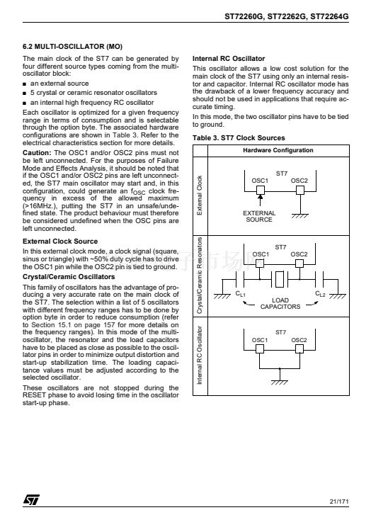
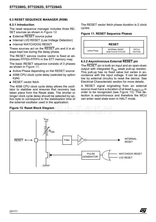
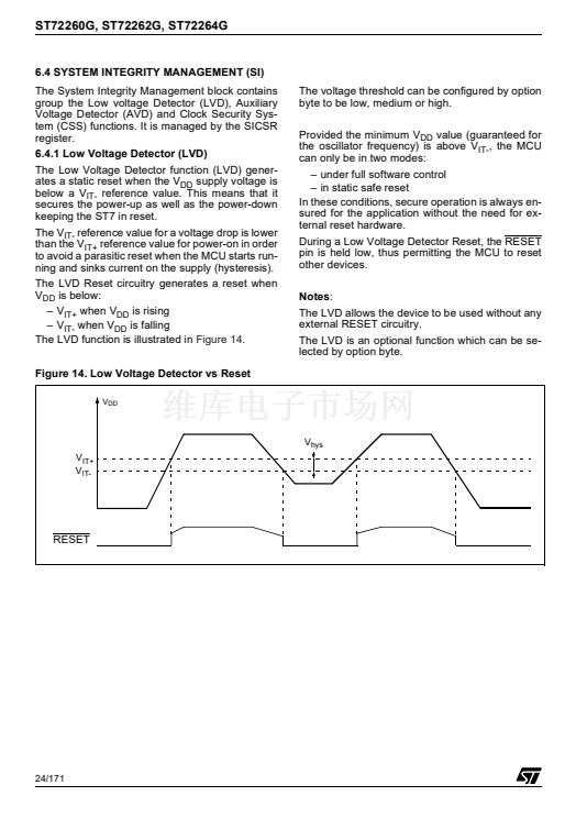
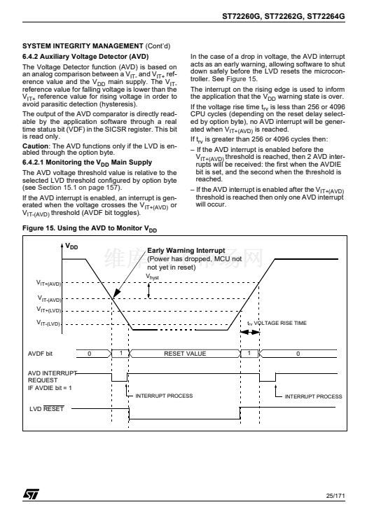
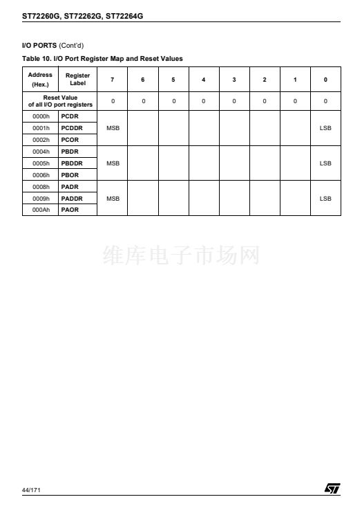
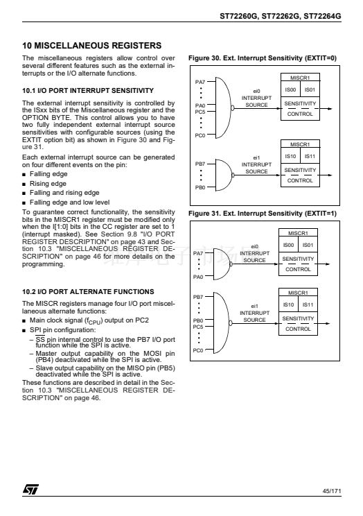
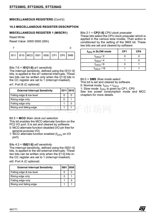
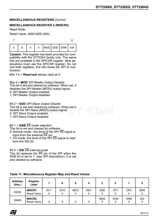
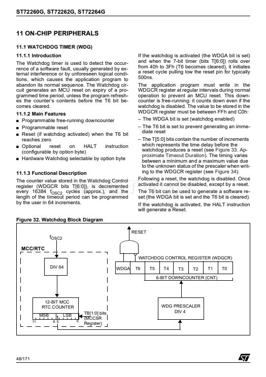
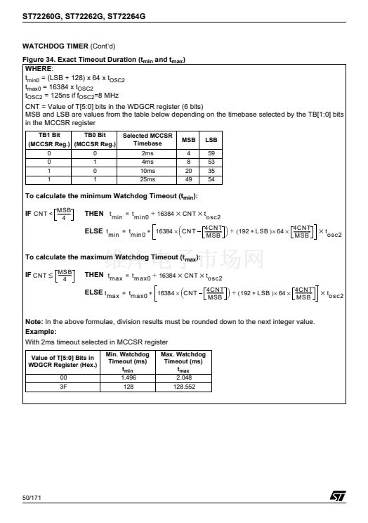
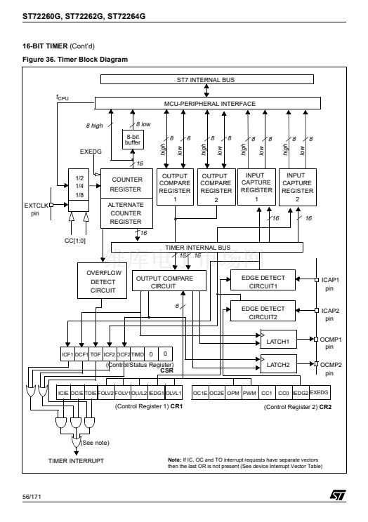
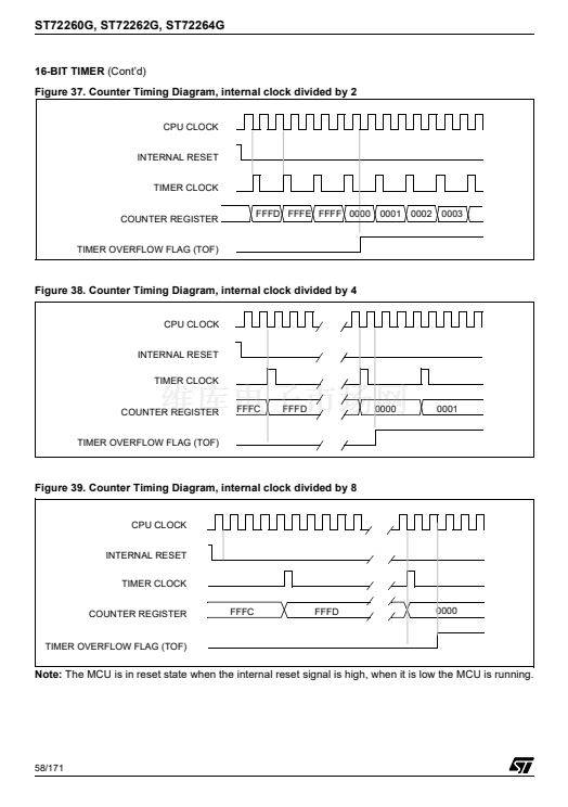
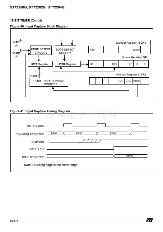
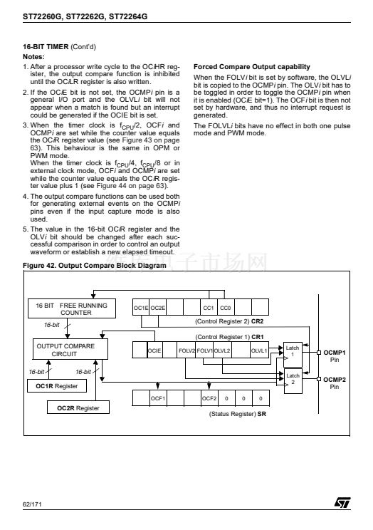
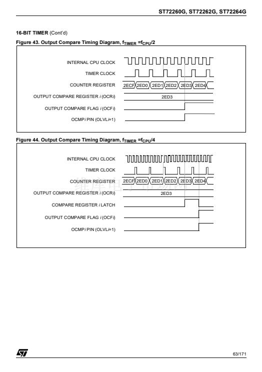
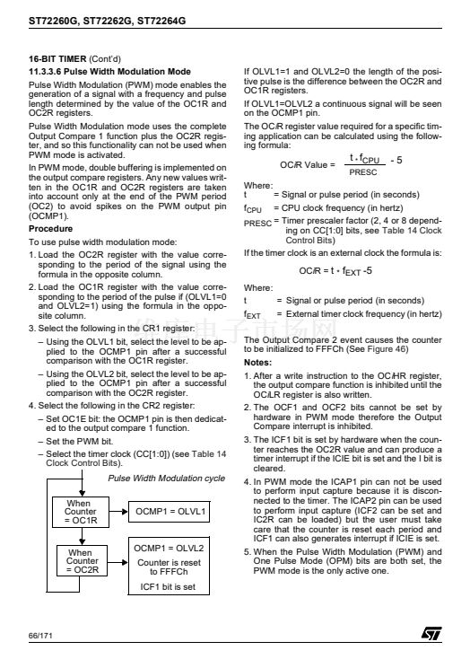
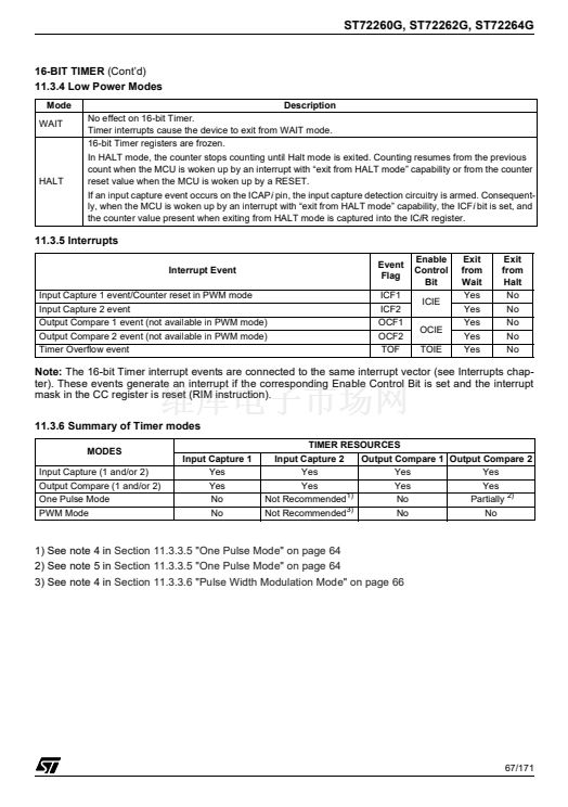
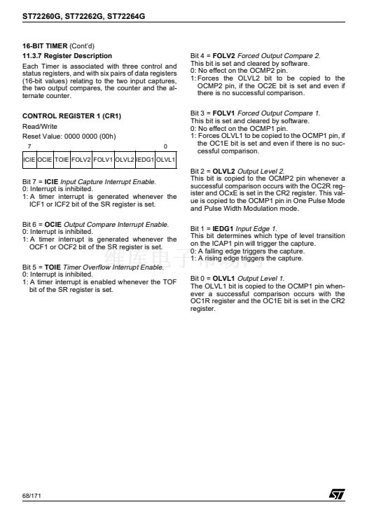
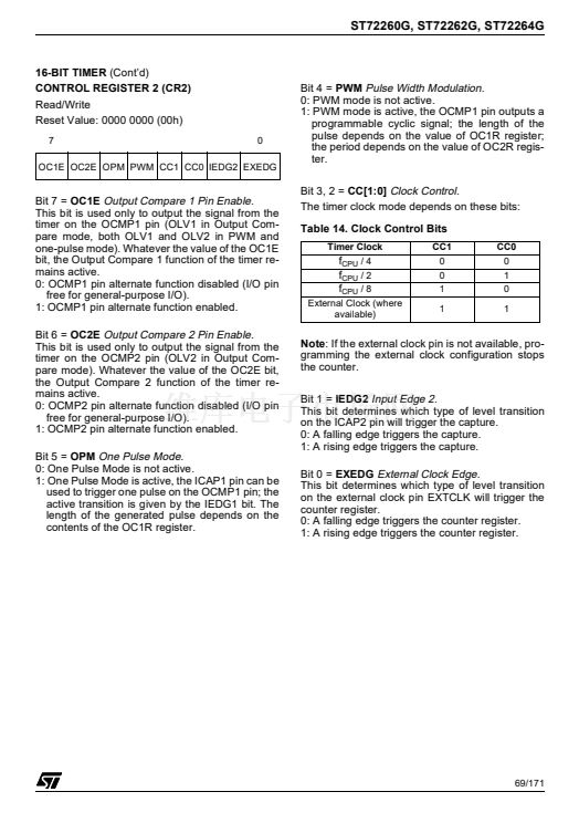
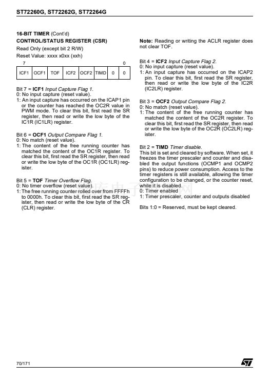
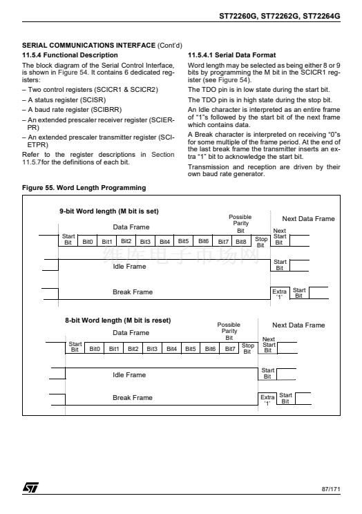
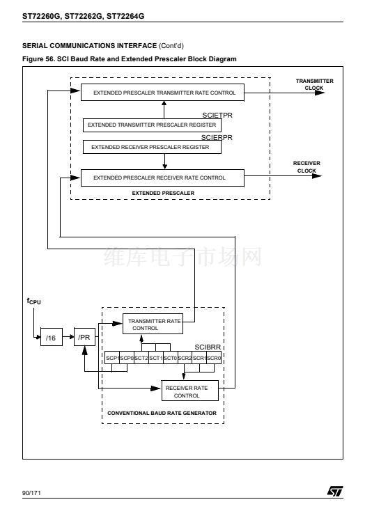
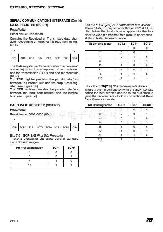
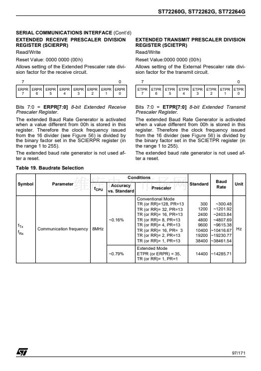
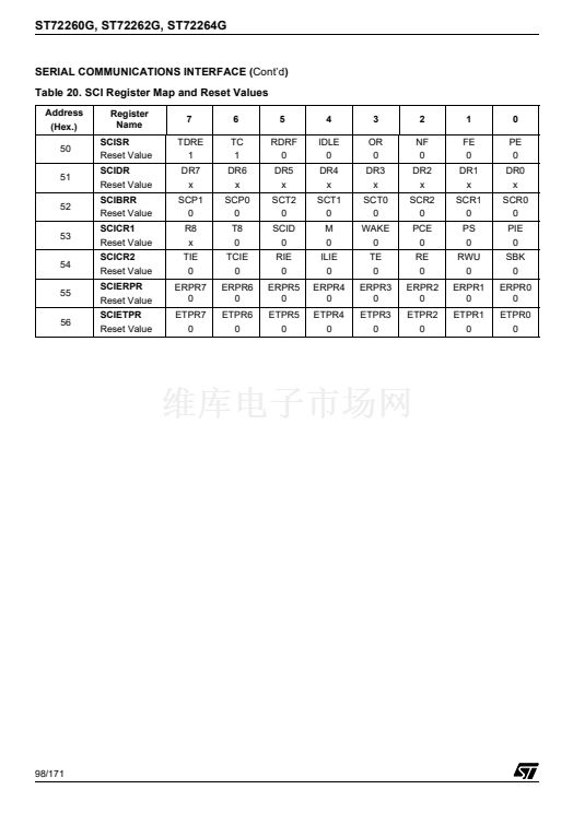
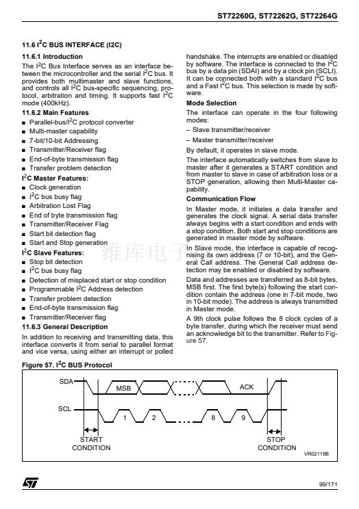
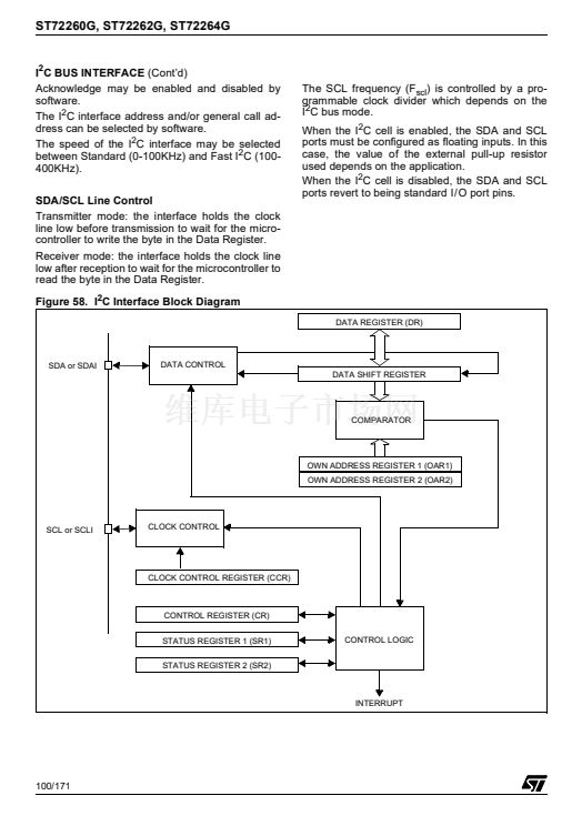
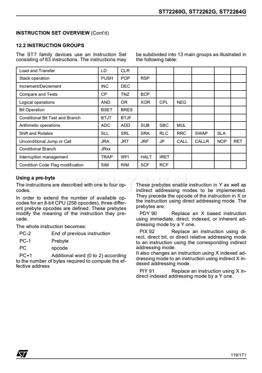
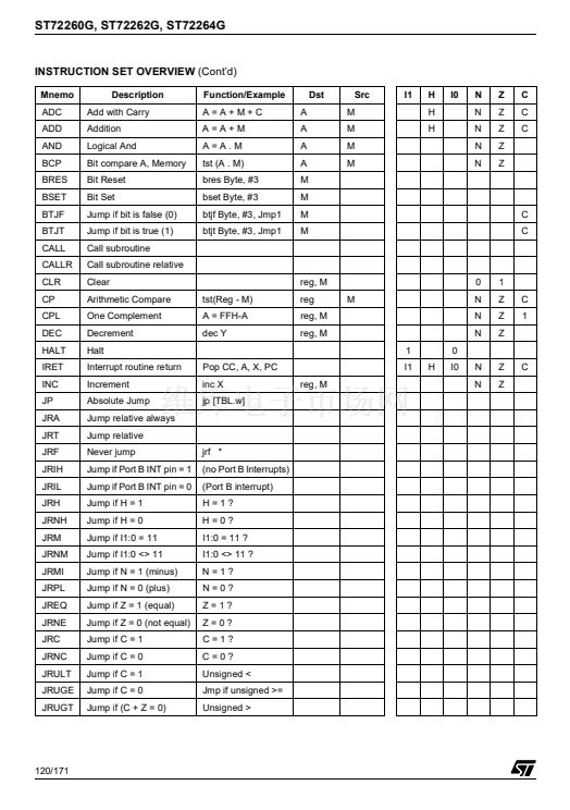
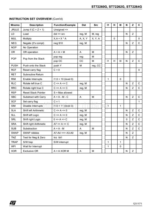
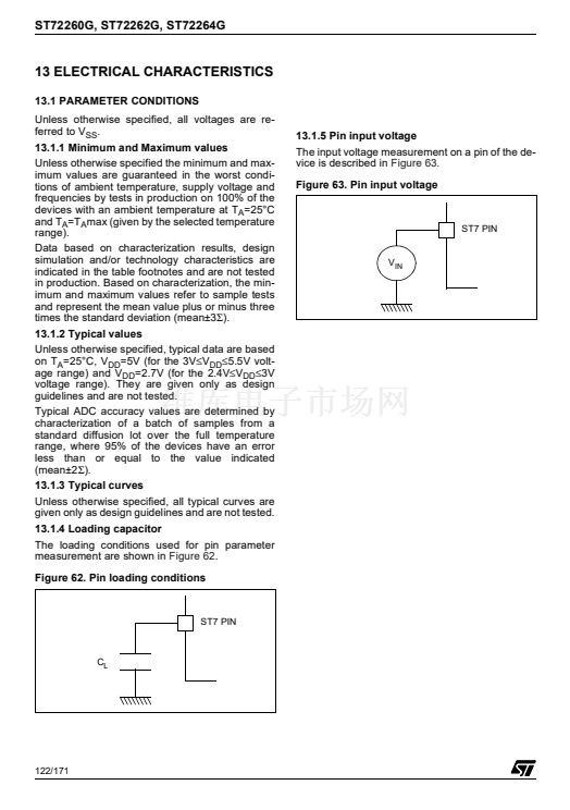
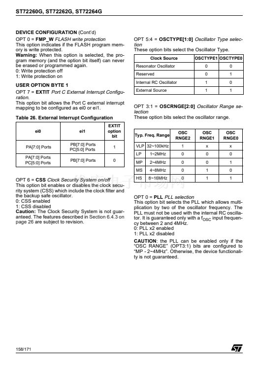
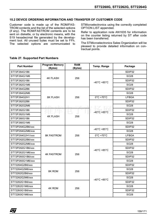
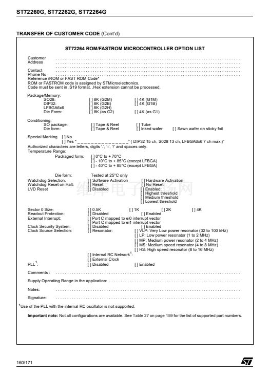
ST72260G, ST72262G, ST72264G
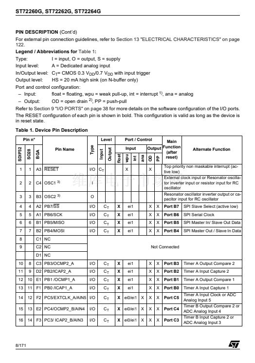
Pin n掳
Type
SDIP32
SO28
BGA
Pin Name
Level
Output
Input
Port / Control
Input
float
wpu
ana
int
OD
PP
Main
Output Function
(after
reset)
X
X
X
X
T
X
T
X
X
X
X
X
Port C2
Port C1
Port C0
Port A7
Port A6
Port A5
Port A4
Alternate Function
17
18
19
20
21
22
23
24
25
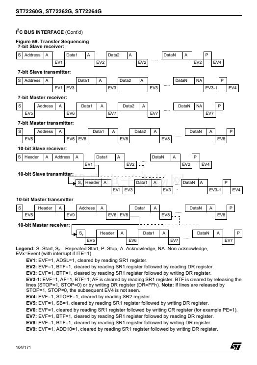
15 E3 PC2/MCO/AIN2
16 F4 PC1/OCMP1_B/AIN1
17 D3 PC0/ICAP1_B/AIN0
18 E4 PA7/TDO
19 F5 PA6/SDAI
20 F6 PA5 /RDI
21 E6 PA4/SCLI
E5 NC
D6 NC
D5 NC
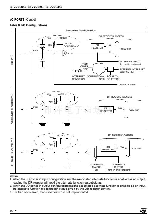
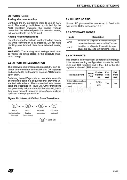
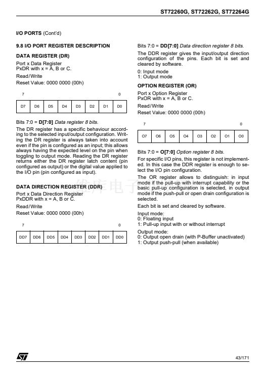
I/O
I/O
I/O
C
T
C
T
C
T
X
ei0/ei1 X
X
ei0/ei1 X
X
ei0/ei1 X
X
X
X
X
ei0
ei0
ei0
ei0
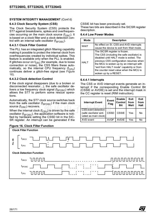
Main clock output (f
CPU
) or
ADC Analog Input 2
Timer B Output Compare 1 or
ADC Analog Input 1
Timer B Input Capture 1 or
ADC Analog Input 0
SCI output
I
2
C DATA
SCI input
I
2
C CLOCK
I/O C
T
HS
I/O C
T
HS
I/O C
T
HS
I/O C
T
HS
Not Connected
26
27
22 C6 PA3
23 D4 PA2
C5 NC
I/O C
T
HS
I/O C
T
HS
X
X
ei0
ei0
X
X
X
X
Port A3
Port A2
Not Connected
B6 NC
28
29
30
31
32
24 A6 PA1/ICCDATA
25 A5 PA0/ICCCLK
26 B5 ICCSEL
27 A4 V
SS
28 B4 V
DD
I/O C
T
HS
I/O C
T
HS
I
S
S
C
T
X
X
X
ei0
ei0
X
X
X
X
Port A1
Port A0
In Circuit Communication Data
In Circuit Communication
Clock
ICC mode pin, must be tied low
Ground
Main power supply
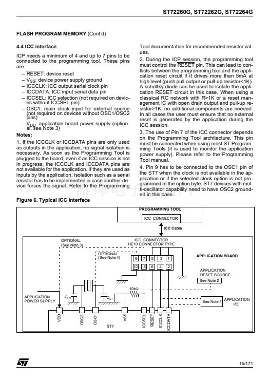
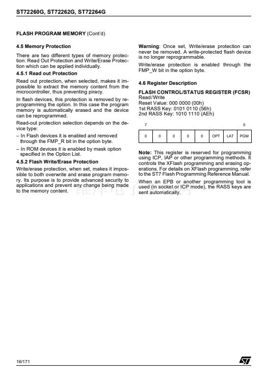
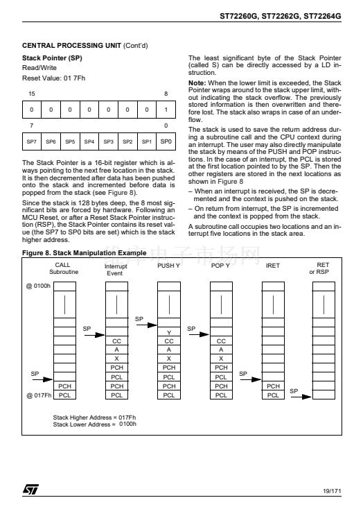
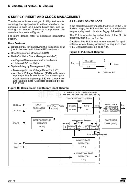
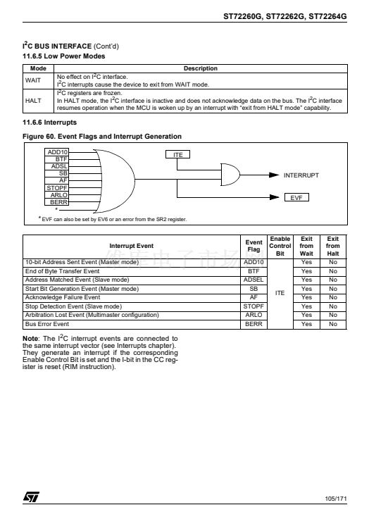
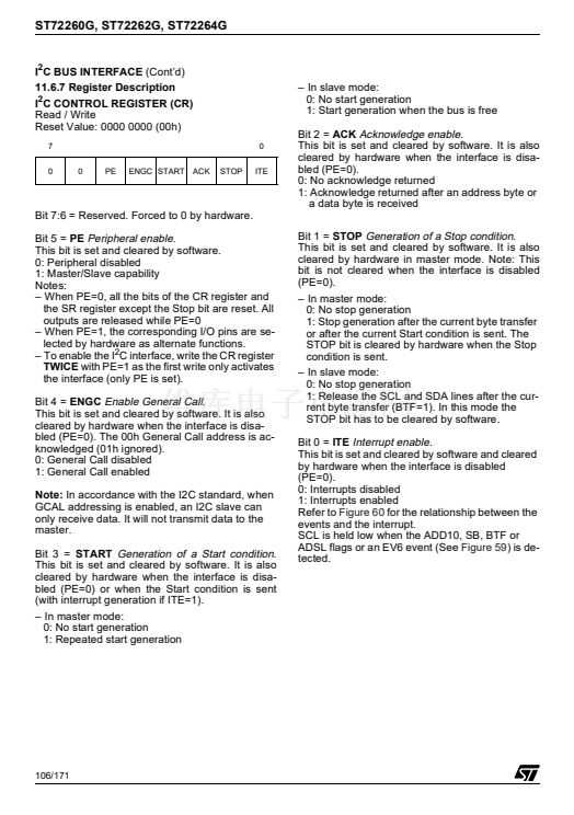
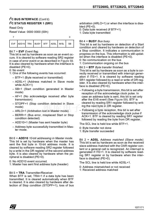
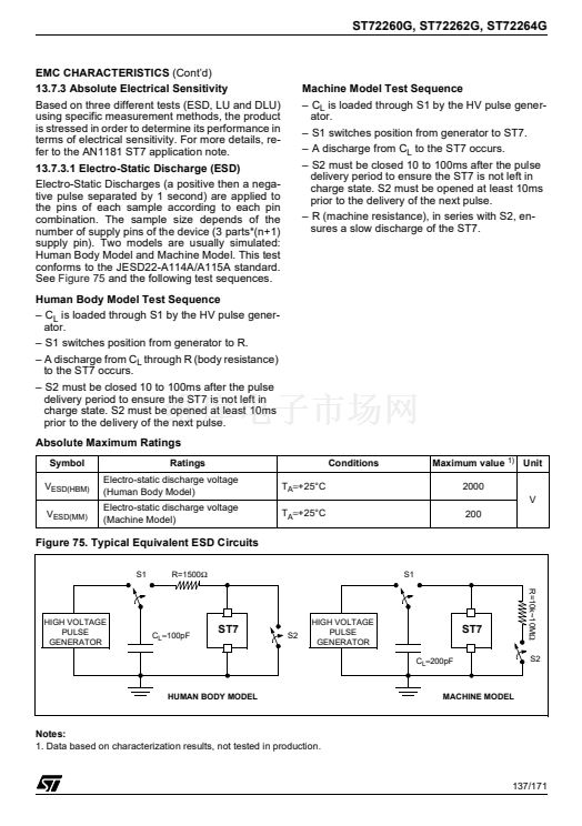
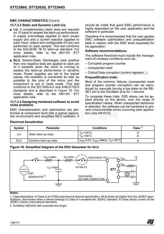
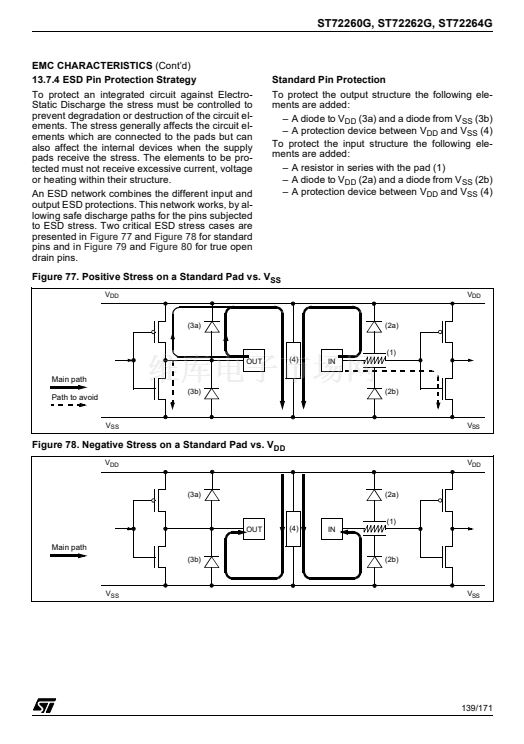
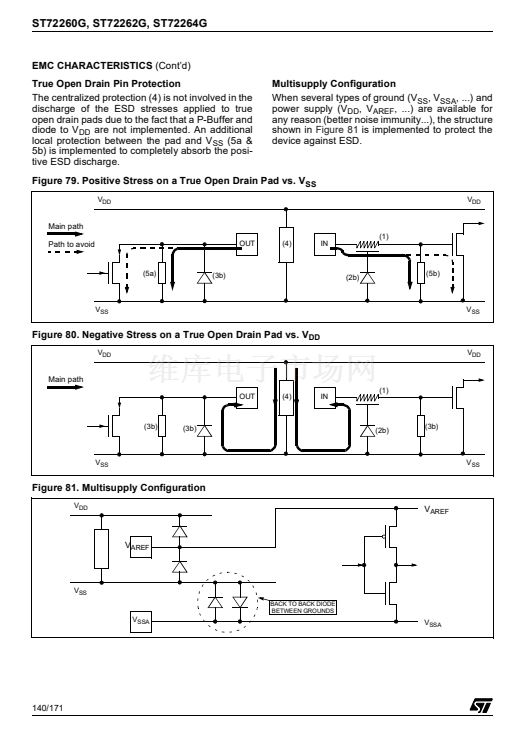
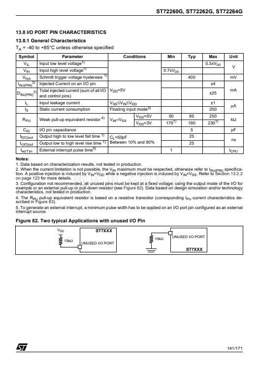
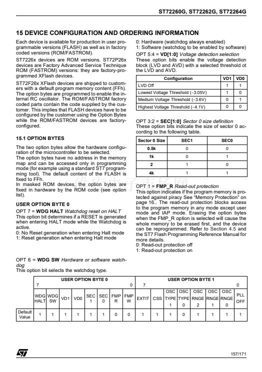
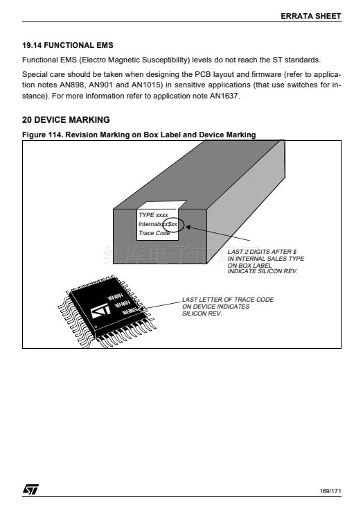
Notes:
1. In the interrupt input column, 鈥渆iX鈥?defines the associated external interrupt vector. If the weak pull-up
column (wpu) is merged with the interrupt column (int), then the I/O configuration is a pull-up interrupt in-
put, otherwise the configuration is a floating interrupt input. Port C is mapped to ei0 or ei1 by option byte.
2. In the open drain output column, 鈥淭鈥?defines a true open drain I/O (P-Buffer and protection diode to V
DD
are not implemented). See
Section 9 "I/O PORTS" on page 38
for more details.
3. OSC1 and OSC2 pins connect a crystal or ceramic resonator, an external RC, or an external source to
the on-chip oscillator see
Section 2 "PIN DESCRIPTION" on page 6
and
Section 6.2 "MULTI-OSCILLA-
TOR (MO)" on page 21
for more details.
9/171


 1
1
 2
2
 3
3
 4
4
 5
5
 6
6
 7
7
 8
8
 9
9
 10
10
 11
11
 12
12
 13
13
 14
14
 15
15
 16
16
 17
17
 18
18
 19
19
 20
20
 21
21
 22
22
 23
23
 24
24
 25
25
 26
26
 27
27
 28
28
 29
29
 30
30
 31
31
 32
32
 33
33
 34
34
 35
35
 36
36
 37
37
 38
38
 39
39
 40
40
 41
41
 42
42
 43
43
 44
44
 45
45
 46
46
 47
47
 48
48
 49
49
 50
50
 51
51
 52
52
 53
53
 54
54
 55
55
 56
56
 57
57
 58
58
 59
59
 60
60
 61
61
 62
62
 63
63
 64
64
 65
65
 66
66
 67
67
 68
68
 69
69
 70
70
 71
71
 72
72
 73
73
 74
74
 75
75
 76
76
 77
77
 78
78
 79
79
 80
80
 81
81
 82
82
 83
83
 84
84
 85
85
 86
86
 87
87
 88
88
 89
89
 90
90
 91
91
 92
92
 93
93
 94
94
 95
95
 96
96
 97
97
 98
98
 99
99
 100
100
 101
101
 102
102
 103
103
 104
104
 105
105
 106
106
 107
107
 108
108
 109
109
 110
110
 111
111
 112
112
 113
113
 114
114
 115
115
 116
116
 117
117
 118
118
 119
119
 120
120
 121
121
 122
122
 123
123
 124
124
 125
125
 126
126
 127
127
 128
128
 129
129
 130
130
 131
131
 132
132
 133
133
 134
134
 135
135
 136
136
 137
137
 138
138
 139
139
 140
140
 141
141
 142
142
 143
143
 144
144
 145
145
 146
146
 147
147
 148
148
 149
149
 150
150
 151
151
 152
152
 153
153
 154
154
 155
155
 156
156
 157
157
 158
158
 159
159
 160
160
 161
161
 162
162
 163
163
 164
164
 165
165
 166
166
 167
167
 168
168
 169
169
 170
170
 171
171
