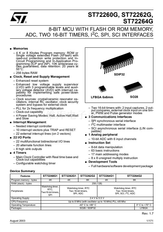
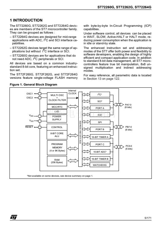
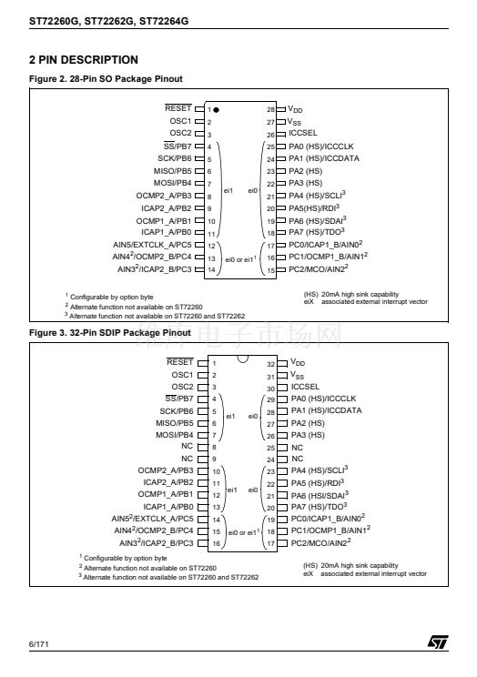
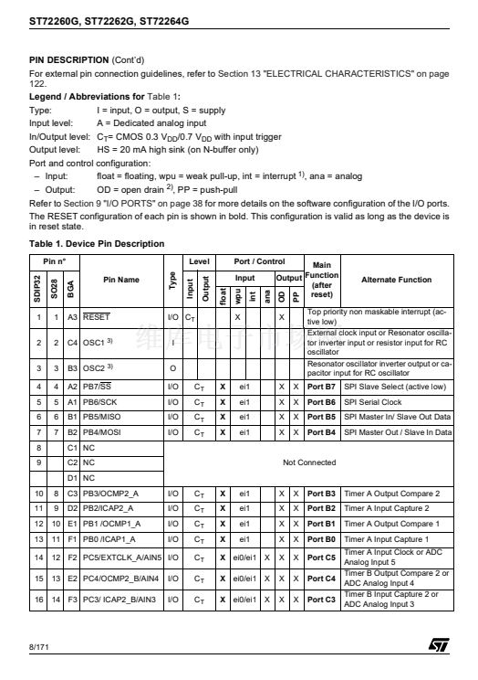
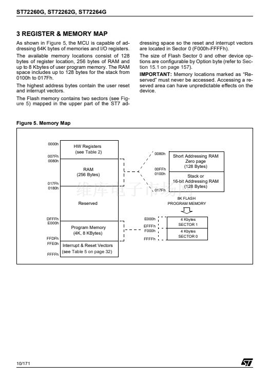
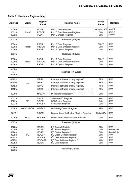
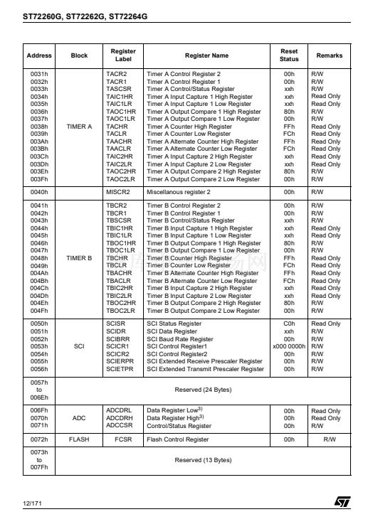
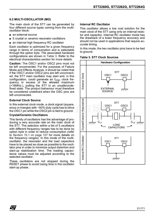
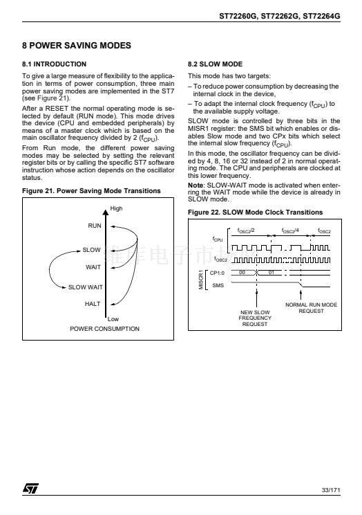
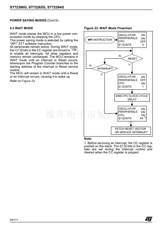
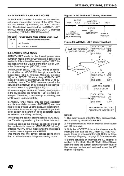
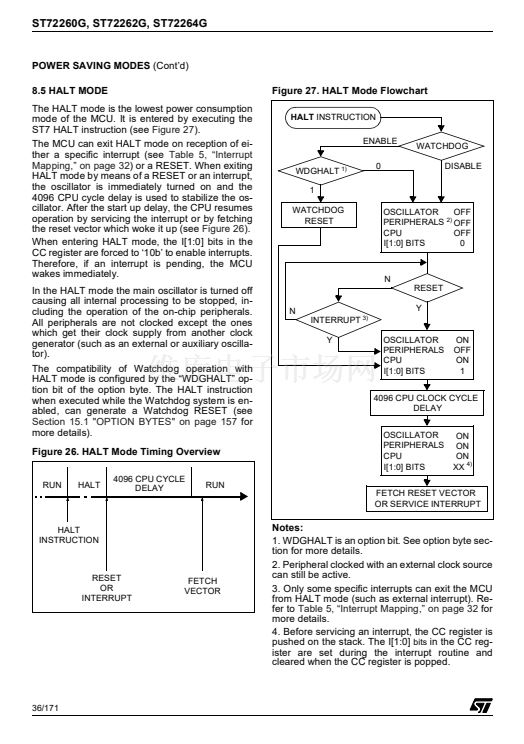
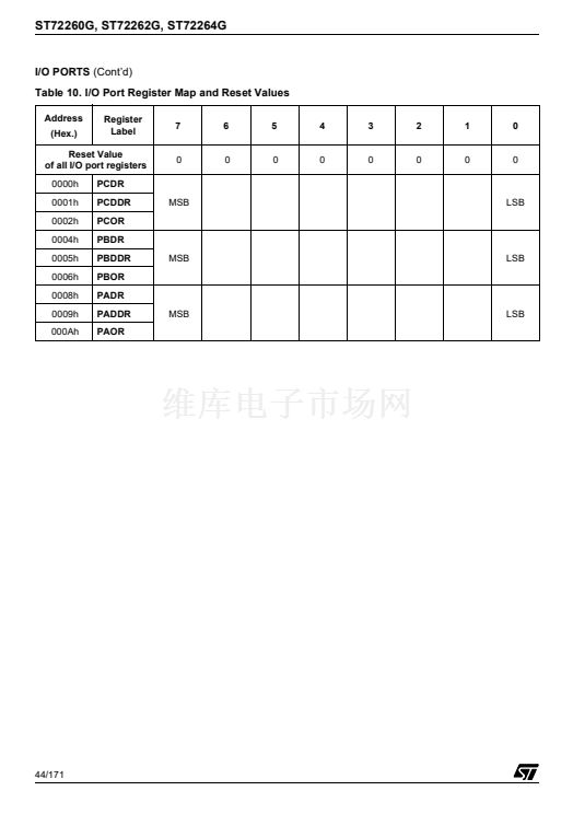
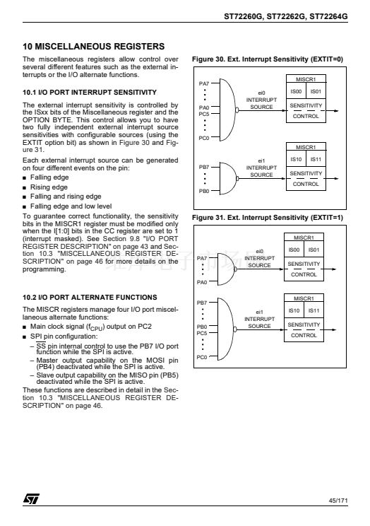
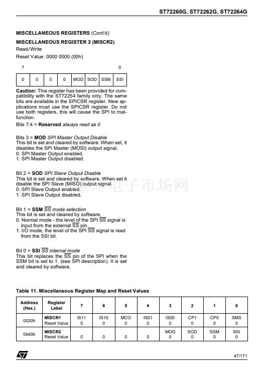
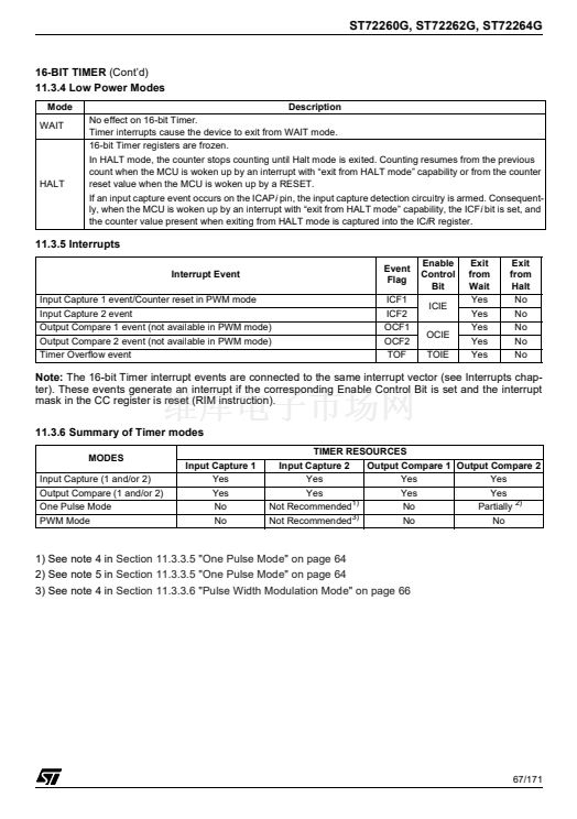
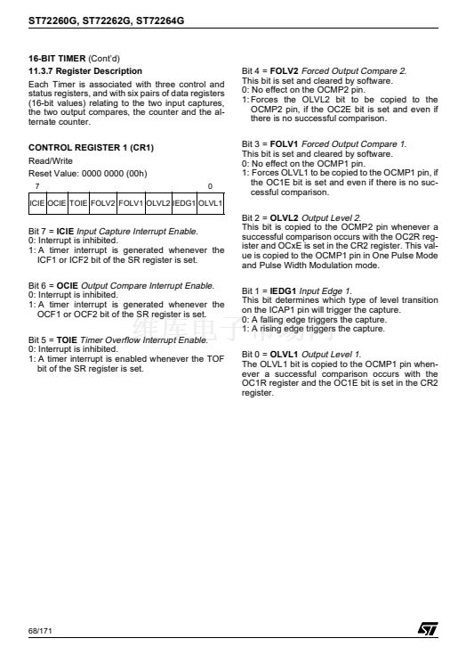
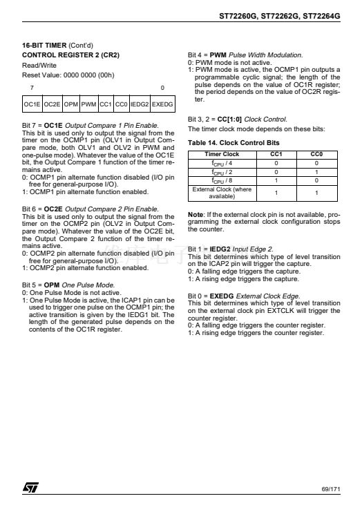
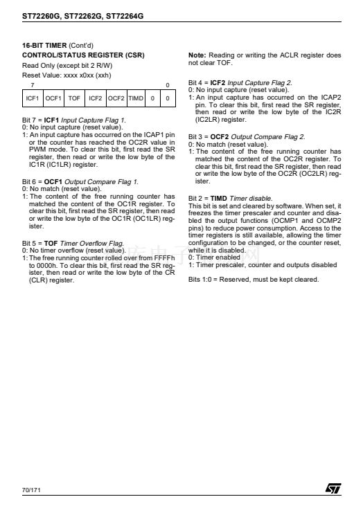
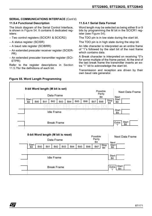
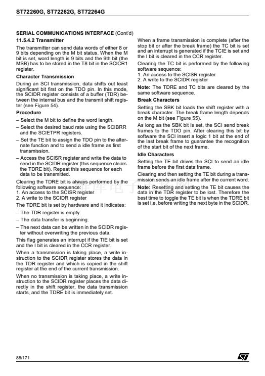
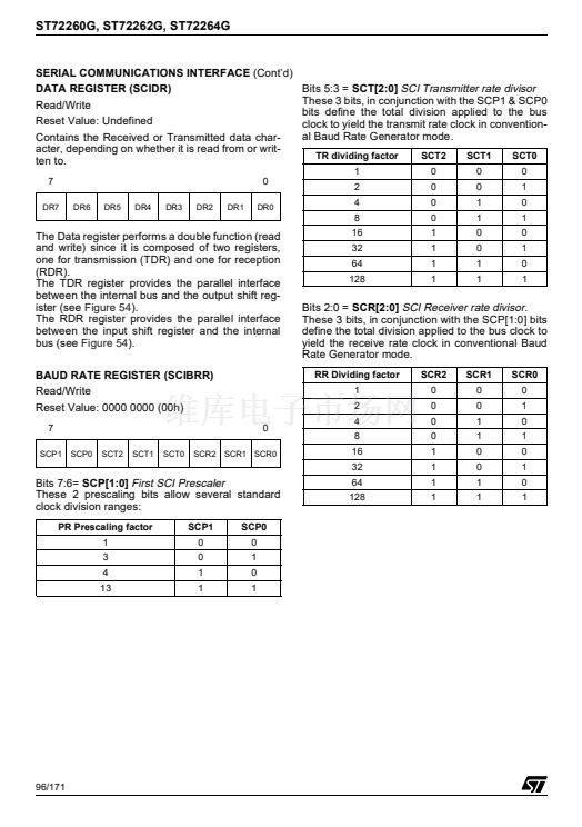
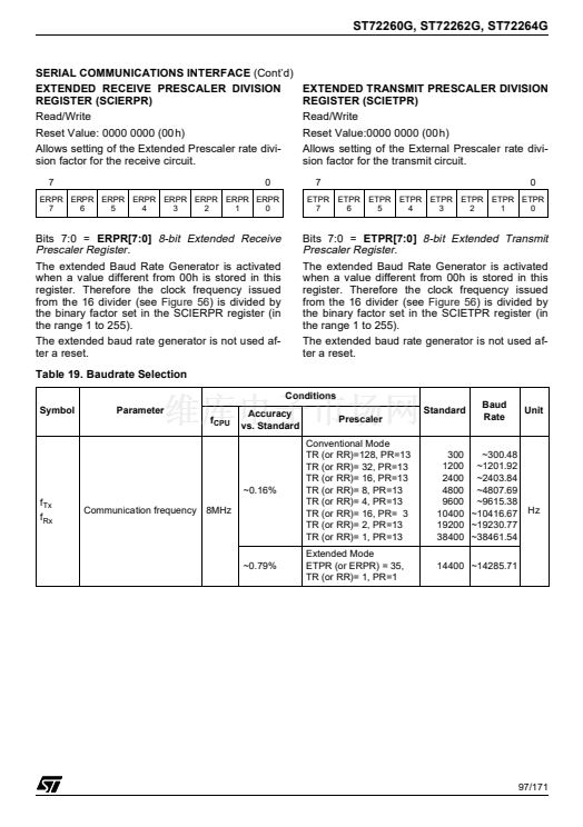
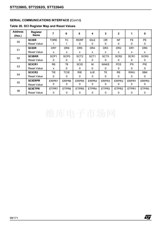
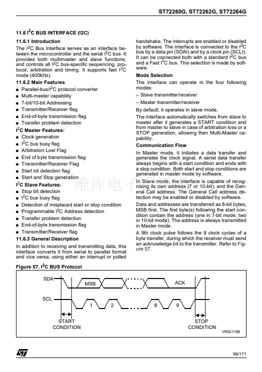
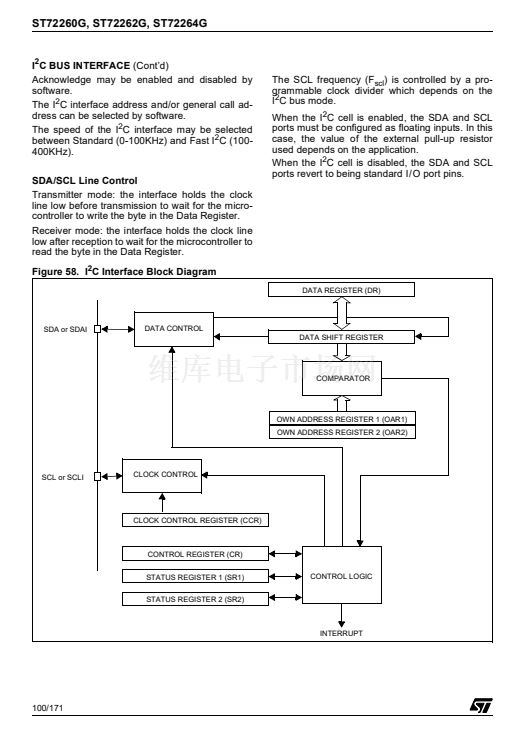
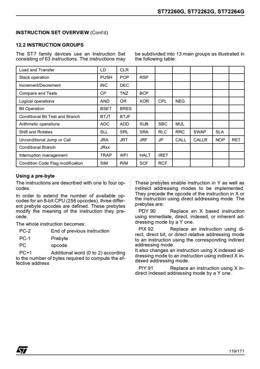
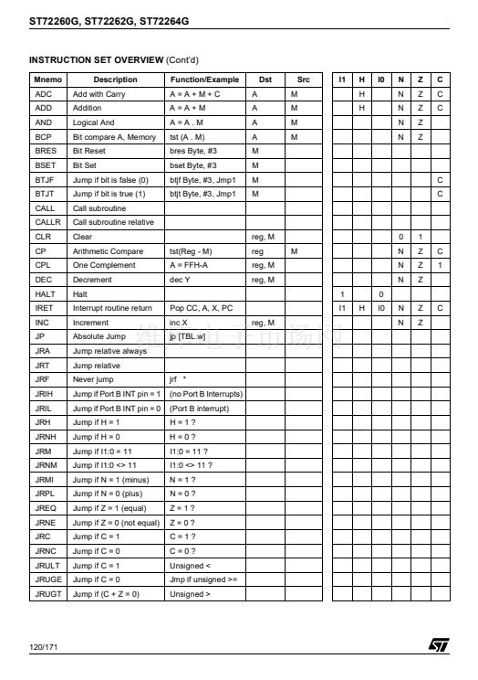
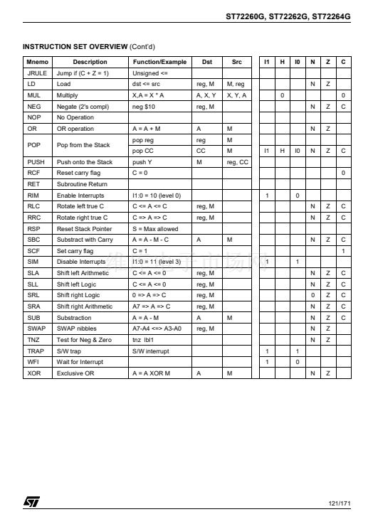
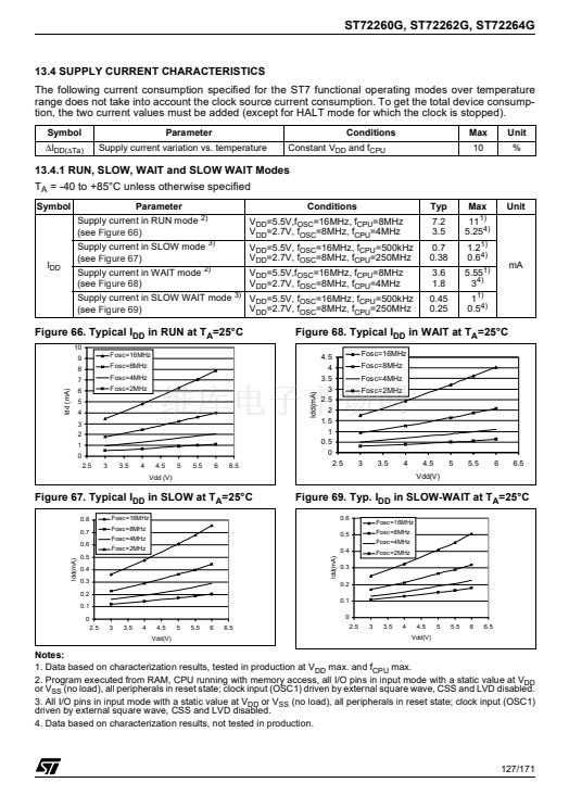
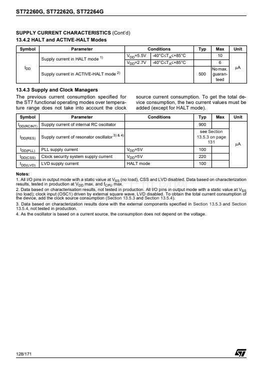
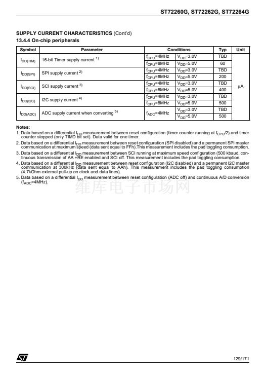
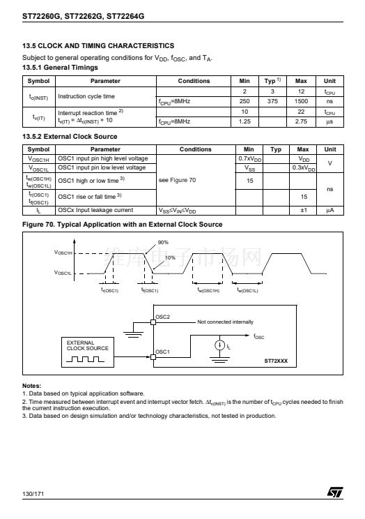
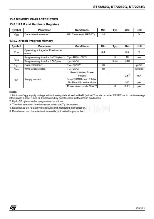
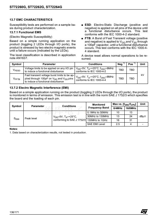
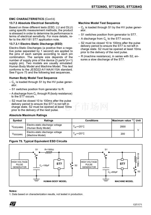
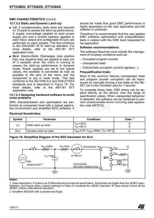
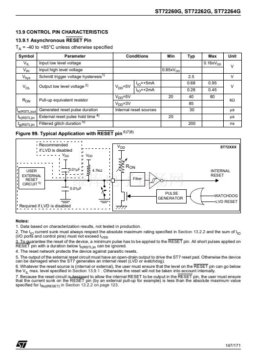
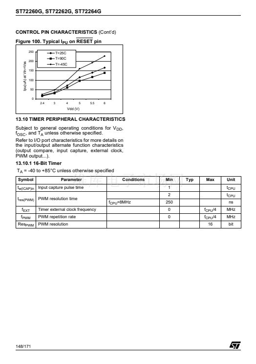
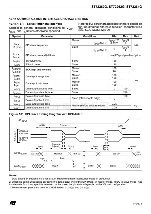
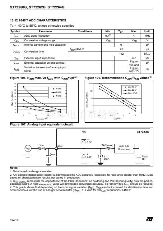
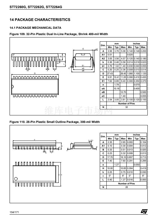
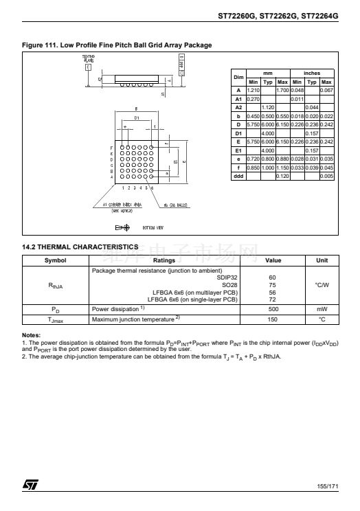
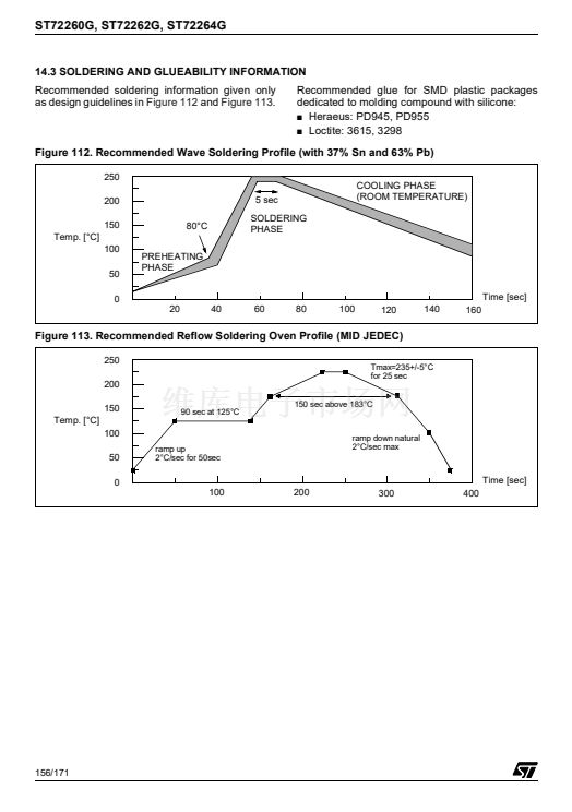
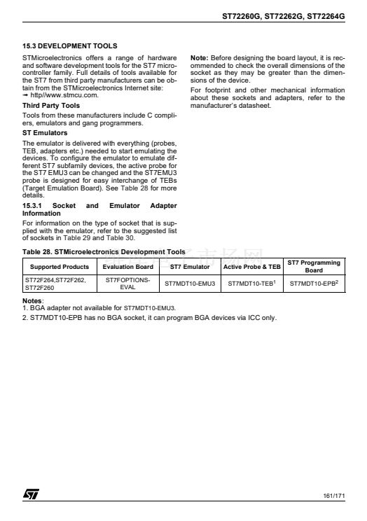
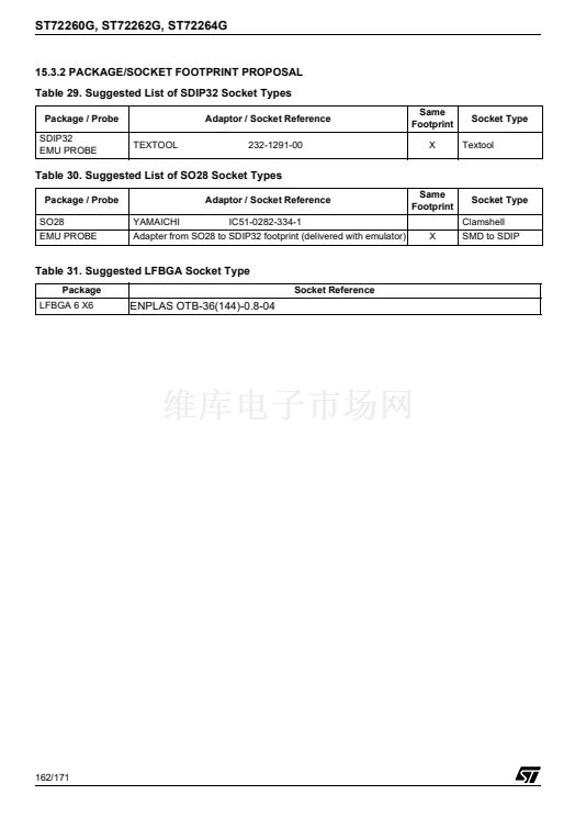
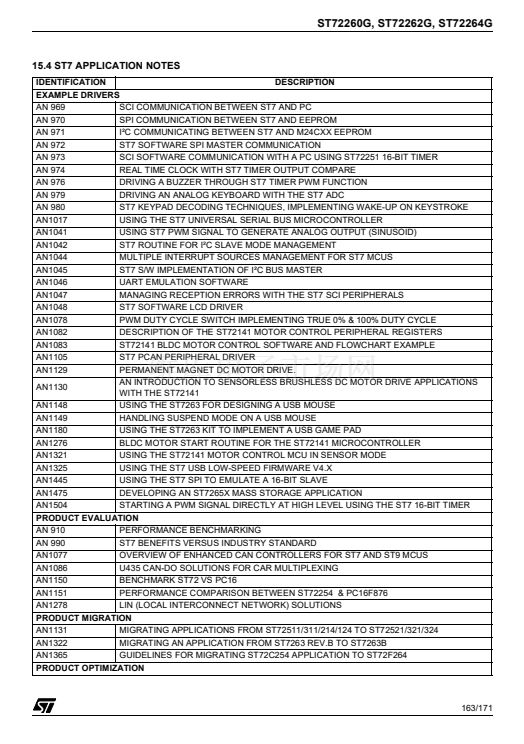
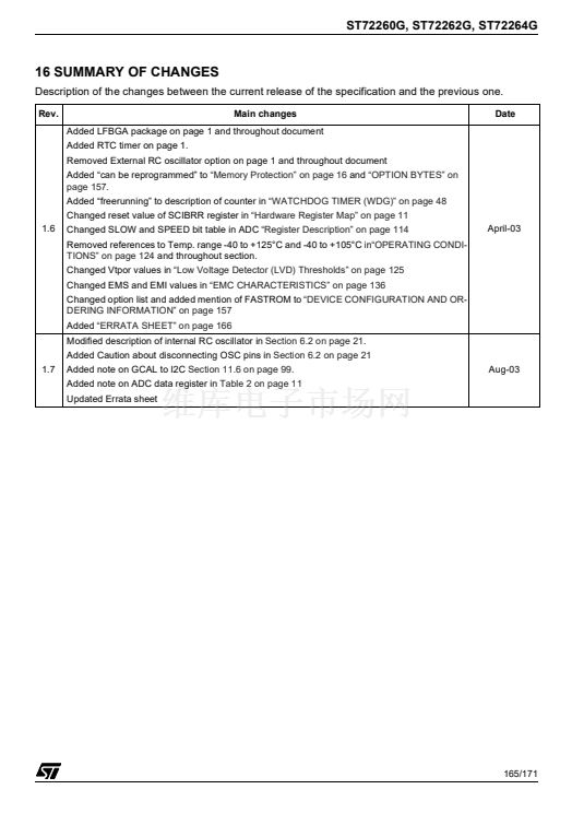
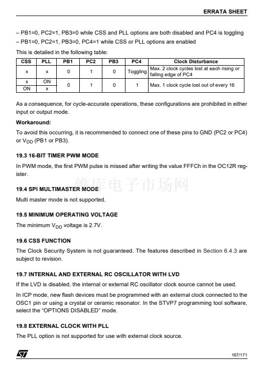
ST72260G, ST72262G, ST72264G
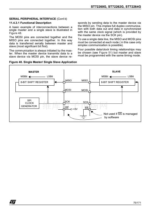
SERIAL PERIPHERAL INTERFACE
(Cont鈥檇)
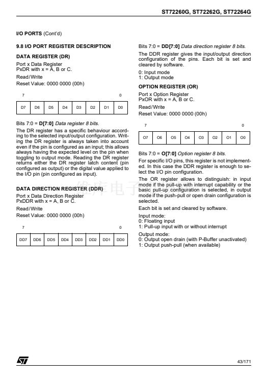
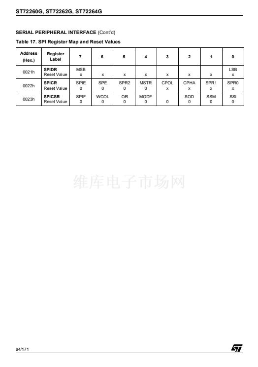
11.4.8 Register Description
CONTROL REGISTER (SPICR)
Read/Write
Reset Value: 0000 xxxx (0xh)
7
SPIE
SPE
SPR2
MSTR
CPOL
CPHA
SPR1
0
SPR0
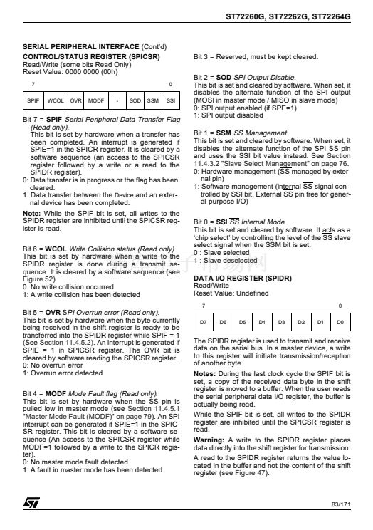
Bit 7 =
SPIE
Serial Peripheral Interrupt Enable.
This bit is set and cleared by software.
0: Interrupt is inhibited
1: An SPI interrupt is generated whenever an End
of Transfer event, Master Mode Fault or Over-
run error occurs (SPIF=1, MODF=1 or OVR=1
in the SPICSR register)
Bit 6 =
SPE
Serial Peripheral Output Enable.
This bit is set and cleared by software. It is also
cleared by hardware when, in master mode, SS=0
(see
Section 11.4.5.1 "Master Mode Fault
(MODF)" on page 79).
The SPE bit is cleared by
reset, so the SPI peripheral is not initially connect-
ed to the external pins.
0: I/O pins free for general purpose I/O
1: SPI I/O pin alternate functions enabled
Bit 5 =
SPR2
Divider Enable.
This bit is set and cleared by software and is
cleared by reset. It is used with the SPR[1:0] bits to
set the baud rate. Refer to
Table 16 SPI Master
mode SCK Frequency.
0: Divider by 2 enabled
1: Divider by 2 disabled
Note:
This bit has no effect in slave mode.
Bit 4 =
MSTR
Master Mode.
This bit is set and cleared by software. It is also
cleared by hardware when, in master mode, SS=0
(see
Section 11.4.5.1 "Master Mode Fault
(MODF)" on page 79).
0: Slave mode
1: Master mode. The function of the SCK pin
changes from an input to an output and the func-
tions of the MISO and MOSI pins are reversed.
Bit 3 =
CPOL
Clock Polarity.
This bit is set and cleared by software. This bit de-
termines the idle state of the serial Clock. The
CPOL bit affects both the master and slave
modes.
0: SCK pin has a low level idle state
1: SCK pin has a high level idle state
Note:
If CPOL is changed at the communication
byte boundaries, the SPI must be disabled by re-
setting the SPE bit.
Bit 2 =
CPHA
Clock Phase.
This bit is set and cleared by software.
0: The first clock transition is the first data capture
edge.
1: The second clock transition is the first capture
edge.
Note:
The slave must have the same CPOL and
CPHA settings as the master.
Bits 1:0 =
SPR[1:0]
Serial Clock Frequency.
These bits are set and cleared by software. Used
with the SPR2 bit, they select the baud rate of the
SPI serial clock SCK output by the SPI in master
mode.
Note:
These 2 bits have no effect in slave mode.
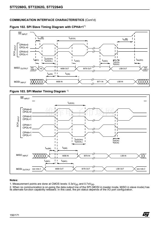
Table 16. SPI Master mode SCK Frequency
Serial Clock
f
CPU
/4
f
CPU
/8
f
CPU
/16
f
CPU
/32
f
CPU
/64
f
CPU
/128
SPR2
1
0
0
1
0
0
SPR1
0
0
0
1
1
1
SPR0
0
0
1
0
0
1
82/171


 1
1
 2
2
 3
3
 4
4
 5
5
 6
6
 7
7
 8
8
 9
9
 10
10
 11
11
 12
12
 13
13
 14
14
 15
15
 16
16
 17
17
 18
18
 19
19
 20
20
 21
21
 22
22
 23
23
 24
24
 25
25
 26
26
 27
27
 28
28
 29
29
 30
30
 31
31
 32
32
 33
33
 34
34
 35
35
 36
36
 37
37
 38
38
 39
39
 40
40
 41
41
 42
42
 43
43
 44
44
 45
45
 46
46
 47
47
 48
48
 49
49
 50
50
 51
51
 52
52
 53
53
 54
54
 55
55
 56
56
 57
57
 58
58
 59
59
 60
60
 61
61
 62
62
 63
63
 64
64
 65
65
 66
66
 67
67
 68
68
 69
69
 70
70
 71
71
 72
72
 73
73
 74
74
 75
75
 76
76
 77
77
 78
78
 79
79
 80
80
 81
81
 82
82
 83
83
 84
84
 85
85
 86
86
 87
87
 88
88
 89
89
 90
90
 91
91
 92
92
 93
93
 94
94
 95
95
 96
96
 97
97
 98
98
 99
99
 100
100
 101
101
 102
102
 103
103
 104
104
 105
105
 106
106
 107
107
 108
108
 109
109
 110
110
 111
111
 112
112
 113
113
 114
114
 115
115
 116
116
 117
117
 118
118
 119
119
 120
120
 121
121
 122
122
 123
123
 124
124
 125
125
 126
126
 127
127
 128
128
 129
129
 130
130
 131
131
 132
132
 133
133
 134
134
 135
135
 136
136
 137
137
 138
138
 139
139
 140
140
 141
141
 142
142
 143
143
 144
144
 145
145
 146
146
 147
147
 148
148
 149
149
 150
150
 151
151
 152
152
 153
153
 154
154
 155
155
 156
156
 157
157
 158
158
 159
159
 160
160
 161
161
 162
162
 163
163
 164
164
 165
165
 166
166
 167
167
 168
168
 169
169
 170
170
 171
171
