铮?/div>
1
F
P2
= -----------------------------------
2蟺
脳
R 3
脳
C3
V
E/A
+
ERROR
AMP
(EQ. 8)
(EQ. 9)
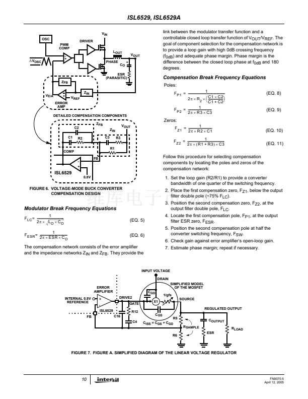
DETAILED COMPENSATION COMPONENTS
Z
FB
Z
IN
C3
R1
R3
V
OUT
Zeros:
1
F
Z1
= -----------------------------------
2蟺
脳
R 2
脳
C1
1
-
F
Z2
= ------------------------------------------------------
2蟺
脳 (
R1 + R3
) 脳
C3
C2
C1
R2
(EQ. 10)
(EQ. 11)
COMP
-
+
FB
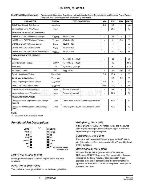
Follow this procedure for selecting compensation
components by locating the poles and zeros of the
compensation network:
1. Set the loop gain (R2/R1) to provide a converter
bandwidth of one quarter of the switching frequency.
2. Place the first compensation zero, F
Z1
, below the output
filter double pole (~75% F
LC
).
3. Position the second compensation zero, F
Z2
, at the
output filter double pole, F
LC
.
(EQ. 5)
(EQ. 6)
4. Locate the first compensation pole, F
P1
, at the output
filter ESR zero, F
ESR
.
5. Position the second compensation pole at half the
converter switching frequency, F
SW
.
6. Check gain against error amplifier鈥檚 open-loop gain.
7. Estimate phase margin; repeat if necessary.
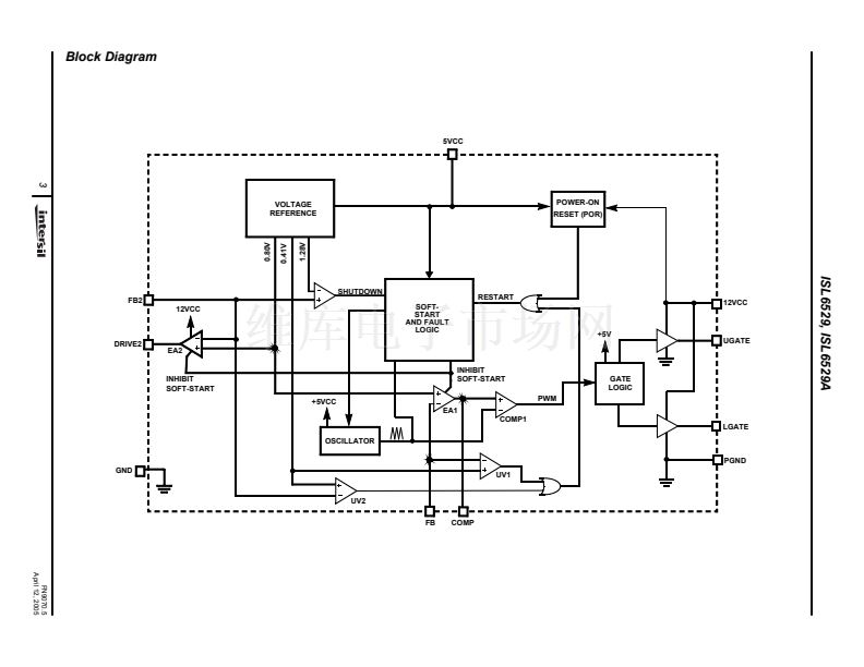
ISL6529
0.8V
FIGURE 6. VOLTAGE-MODE BUCK CONVERTER
COMPENSATION DESIGN
Modulator Break Frequency Equations
1
-
F
LC
= ---------------------------------------
2蟺
脳
L
O
脳
C
O
1
-
F
ESR
= ----------------------------------------
2蟺
脳
ESR
脳
C
O
The compensation network consists of the error amplifier
and the impedance networks Z
IN
and Z
FB
. They provide the
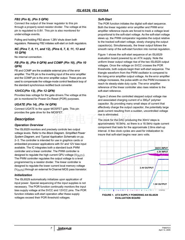
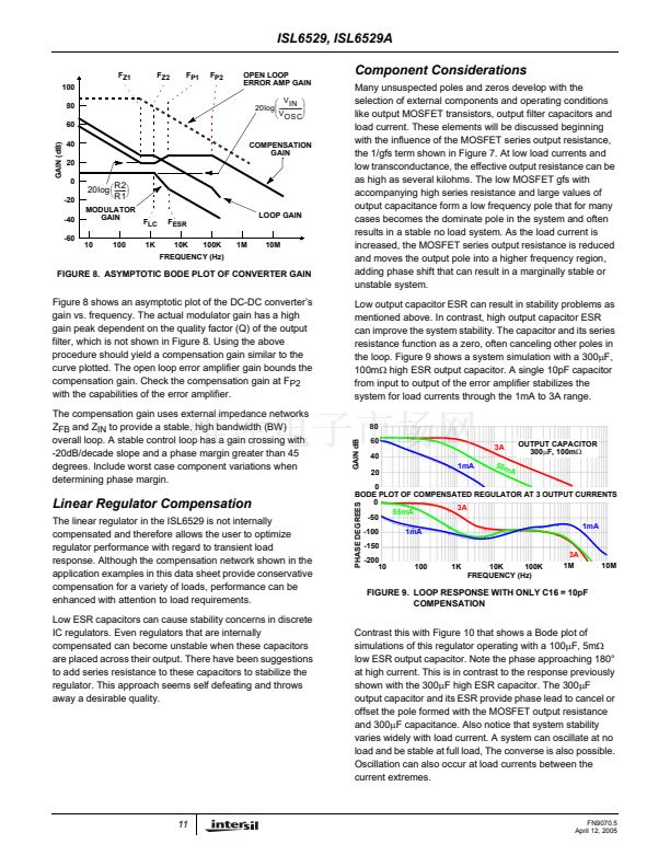
INPUT VOLTAGE
DRAIN
ERROR
AMPLIFIER
INTERNAL 0.8V
REFERENCE
+
-
ISL6529
FB
C16
C4
DRIVE2
GATE
R12
X1
SIMPLIFIED MODEL
OF THE MOSFET
C
GD
1/gfs
SOURCE
REGULATED OUTPUT
R5
C
ISS
= C
GS
+ C
GD
R6
C
GS
C
OUTPUT
R
SAMPLE
ESR
R
LOAD
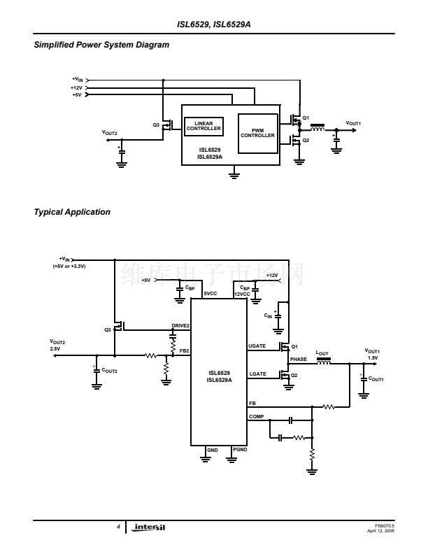
FIGURE 7. FIGURE A. SIMPLIFIED DIAGRAM OF THE LINEAR VOLTAGE REGULATOR
10
FN9070.5
April 12, 2005


 1
1
 2
2
 3
3
 4
4
 5
5
 6
6
 7
7
 8
8
 9
9
 10
10
 11
11
 12
12
 13
13
 14
14
 15
15
 16
16
 17
17
 18
18
 19
19
