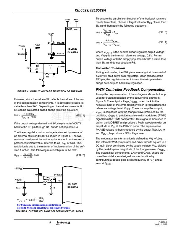
鈥?/div>
V
REF
12VCC 5VCC
+3.3V
(EQ. 3)
V
OUT1
+
L
OUT
Q1
UGATE
(EQ. 4)
C
OUT1
Q2
LGATE
ISL6529
ISL6529A
FB
R3
R1
C3
C1
C2
COMP
where V
OUT2
is the desired linear regulator output voltage
and V
REF
is the internal reference voltage, 0.8V. For an
output voltage of 0.8V, simply populate R5 with a value less
than 5k鈩?and do not populate R6.
Converter Shutdown
Pulling and holding the FB2 pin above a typical threshold of
1.28V will shut down both regulators. Upon release of the
FB2 pin, the regulators enter into a soft-start cycle which
brings both outputs back into regulation.
R2
R4
FIGURE 4. OUTPUT VOLTAGE SELECTION OF THE PWM
PWM Controller Feedback Compensation
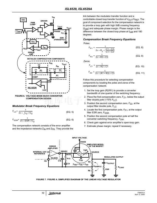
A simplified representation of the voltage-mode control loop
used for output regulation by the converter is shown in
Figure 6. The output voltage, V
OUT
, is fed back to the
negative input of the error amplifier which is regulated to the
reference voltage level, V
REF
. The error amplifier output,
V
E/A
, is compared with the triangle wave produced by the
oscillator, V
OSC
, to provide a pulse-width modulated (PWM)
signal from the PWM comparator. This signal is then used to
switch the MOSFET and produce a PWM waveform with an
amplitude of V
IN
at the PHASE node. The square-wave
PHASE voltage is then smoothed by the output filter, L
OUT
and C
OUT
, to produce a DC voltage level.
The modulator transfer function is defined as V
OUT
/V
E/A
.
The internal PWM comparator and driver circuits equate to a
DC gain block dominated by the supply voltage, V
IN
, divided
by the peak-to-peak magnitude of the triangle wave,
鈭?/div>
V
OSC
.
The output filter components, L
OUT
and C
OUT
, shape the
overall modulator small-signal transfer function by
contributing a double pole break frequency at F
LC
and a
zero at F
ESR
.
However, since the value of R1 affects the values of the rest
of the compensation components, it is advisable to keep its
value less than 5k鈩? Depending on the value chosen for R1,
R4 can be calculated based on the following equation:
R1
脳
0.8V
-
R4 = -------------------------------------
V
OUT1
鈥?/div>
0.8V
(EQ. 1)
If the output voltage desired is 0.8V, simply route VOUT1
back to the FB pin through R1, but do not populate R4.
The linear regulator output voltage is also set by means of
an external resistor divider as shown in Figure 5. The two
resistors used to set the output voltage should not exceed a
parallel equivalent value, referred to as R
FB
, of 5k鈩? This
restriction is due to the manner of implementation of the soft-
start function. The following relationship must be met:
R5
脳
R6
-
R
FB
=
---------------------
<
5k鈩?/div>
R5
+
R6
(EQ. 2)
+3.3V
IN
Q3
R12
V
OUT2
+
R5
R6
DRIVE2
C4
FB2
C
OUT2
ISL6529
ISL6529A
R5
V
OUT2
= 0.8
脳 铮?/div>
1 + -------
铮?/div>
-
铮?/div>
R6
铮?/div>
For frequency compensation considerations
set R5 to 4.64k and adjust R6 for the required voltage.
FIGURE 5. OUTPUT VOLTAGE SELECTION OF THE LINEAR
9
FN9070.5
April 12, 2005
ISL6529CB 产品属性
50
集成电路 (IC)
PMIC - 稳压器 - 线性 + 切换式
-
降压(降压)同步(1),线性(LDO)(1)
任何功能
2
600kHz
0.8 V ~ 3.3 V,15A
0.8 V ~ 3.3 V,4A
-
无
无
无
3.3V,5V
0°C ~ 70°C
表面贴装
14-SOIC(0.154",3.90mm 宽)
14-SOICN
-
ISL6529CB相关型号PDF文件下载
-
型号
版本
描述
厂商
下载
-
英文版
Current Regulated PCI Hot Plug Power Switch Controller
-
英文版
Dual Slot PCI-Express Power Controller
-
英文版
Dual Slot PCI-E Hot Plug Controllers
-
英文版
Power Distribution Controllers
-
英文版
Power Distribution Controllers
-
英文版
Power Distribution Controllers
-
英文版
Dual Power Supply Controller
-
英文版
USB Dual Port Power Supply Controller
-
英文版
Power Distribution Controllers
-
英文版
Single Supply Integrated Current Limiting Controller
-
英文版
Power Sequencing Controllers
-
英文版
Power Sequencing Controllers
-
英文版
Power Sequencing Controllers
-
英文版
Power Sequencing Controllers
-
英文版
Power Sequencing Controllers
-
英文版
Power Sequencing Controllers
-
英文版
Power Sequencing Controllers
-
英文版
Power Sequencing Controllers
INTERSIL [Inter...
-
英文版
Multiple Voltage Supervisory ICs
-
英文版
Multiple Voltage Supervisory ICs
INTERSIL [...


 1
1
 2
2
 3
3
 4
4
 5
5
 6
6
 7
7
 8
8
 9
9
 10
10
 11
11
 12
12
 13
13
 14
14
 15
15
 16
16
 17
17
 18
18
 19
19
