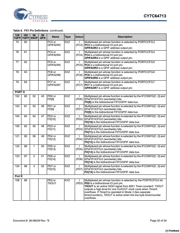
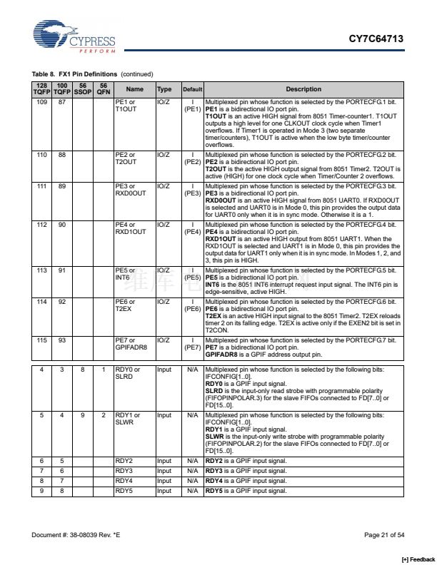
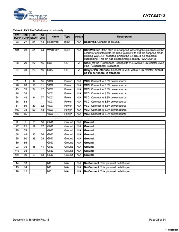
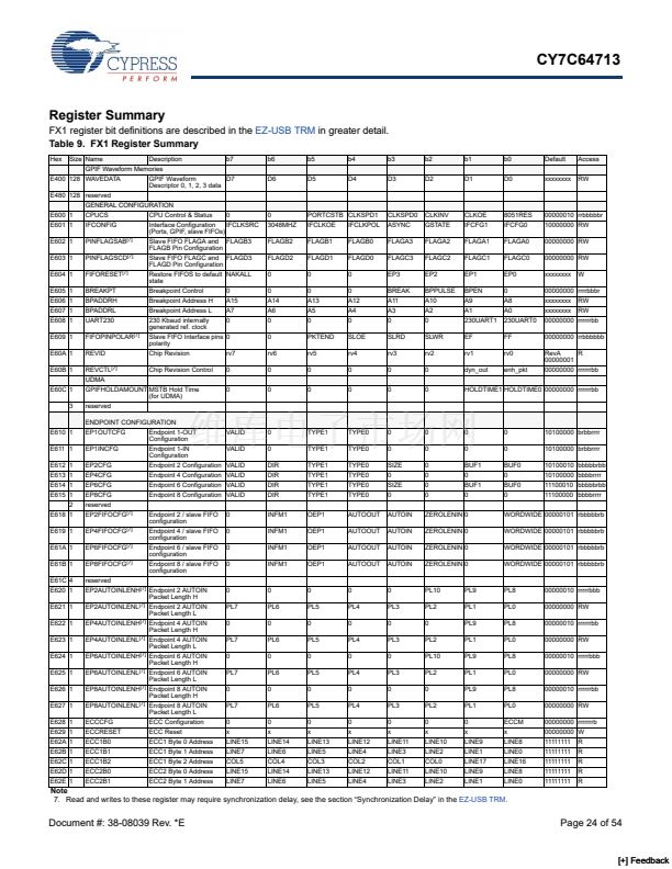
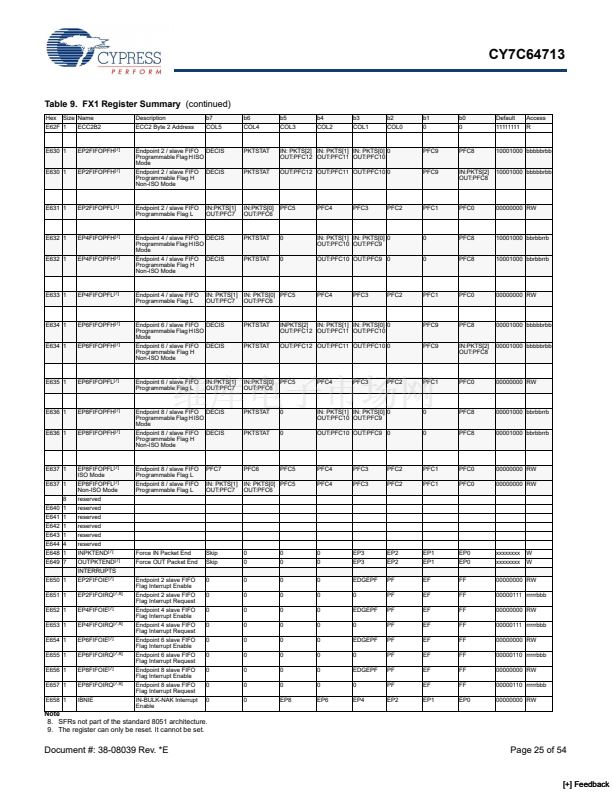
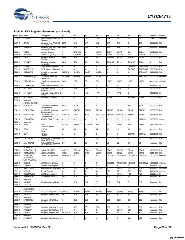
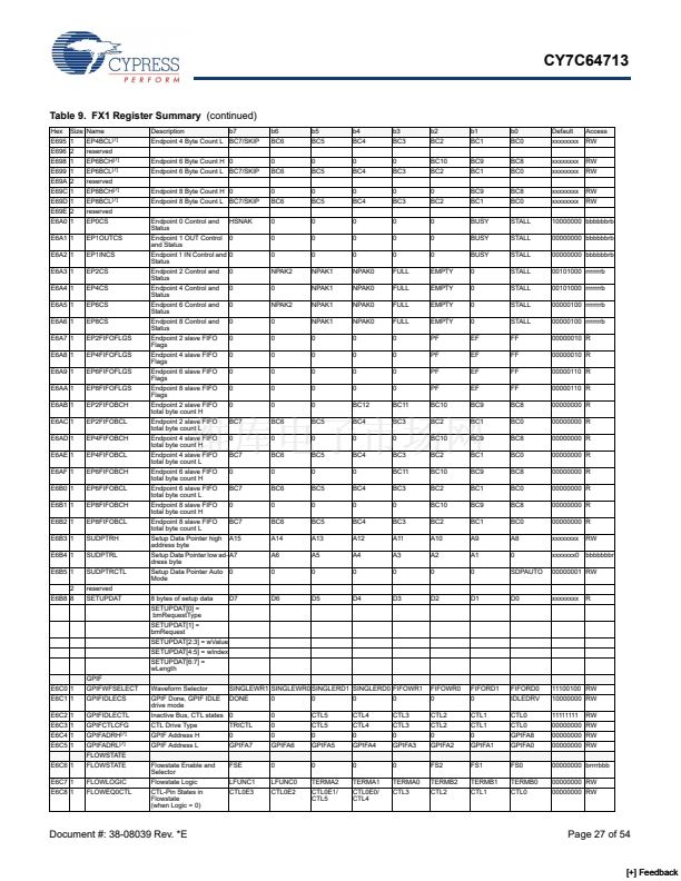
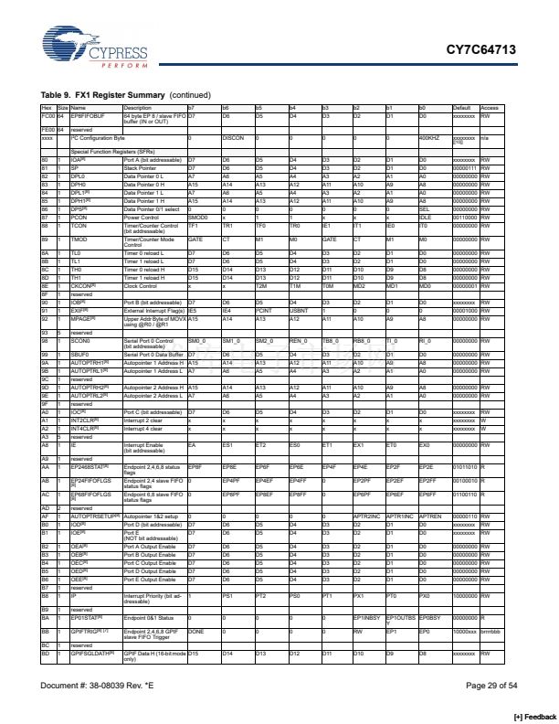
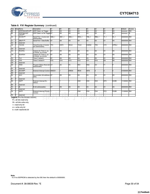
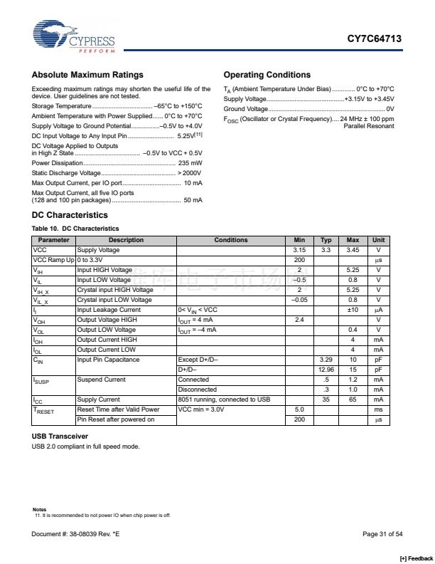
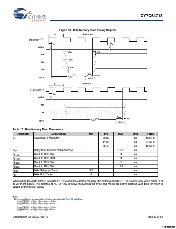
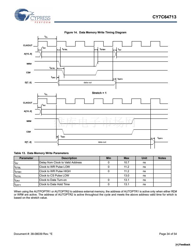
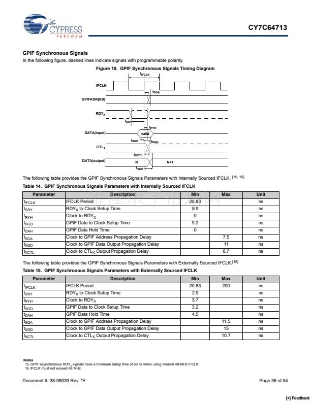
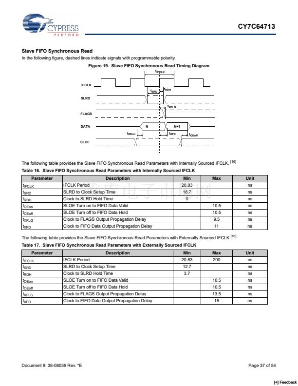
CY7C64713
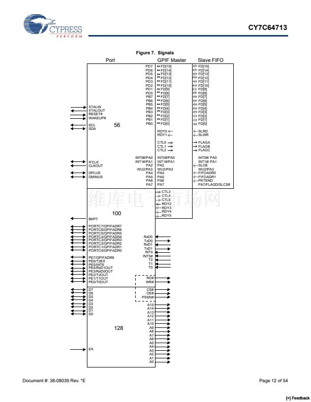
Master/Slave Control Signals
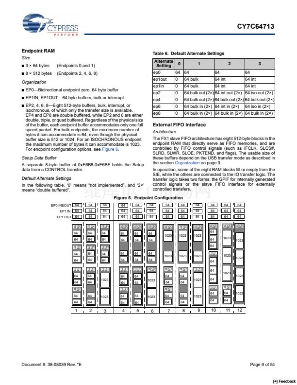
The FX1 endpoint FIFOS are implemented as eight physically
distinct 256x16 RAM blocks. The 8051/SIE can switch any of
the RAM blocks between two domains: the USB (SIE) domain
and the 8051-IO Unit domain. This switching is done
instantaneously, giving essentially zero transfer time between
鈥淯SB FIFOS鈥?and 鈥淪lave FIFOS.鈥?While they are physically the
same memory, no bytes are actually transferred between
buffers.
At any time, some RAM blocks fil or empty with USB data
under SIE control, while other RAM blocks are available to the
8051 and the IO control unit. The RAM blocks operate as a
single-port in the USB domain, and dual port in the 8051-IO
domain. The blocks are configured as single, double, triple, or
quad buffered.
The IO control unit implements either an internal master (M for
master) or external master (S for Slave) interface.
In Master (M) mode, the GPIF internally controls
FIFOADR[1..0] to select a FIFO. The RDY pins (two in the 56
pin package, six in the 100 pin and 128 pin packages) are used
as flag inputs from an external FIFO or other logic if desired.
The GPIF is run from either an internally derived clock or an
externally supplied clock (IFCLK), at a rate that transfers data
up to 96 Megabytes/s (48 MHz IFCLK with 16-bit interface).
In Slave (S) mode, the FX1 accepts either an internally derived
clock or an externally supplied clock (IFCLK with a maximum
frequency of 48 MHz) and SLCS#, SLRD, SLWR, SLOE,
PKTEND signals from external logic. When using an external
IFCLK, the external clock must be present before switching to
the external clock with the IFCLKSRC bit. Each endpoint can
individually be selected for byte or word operation by an
internal configuration bit, and a Slave FIFO Output Enable
signal SLOE enables data of the selected width. External logic
must ensure that the output enable signal is inactive when
writing data to a slave FIFO. The slave interface can also
operate asynchronously, where the SLRD and SLWR signals
act directly as strobes, rather than a clock qualifier as in the
synchronous mode. The signals SLRD, SLWR, SLOE, and
PKTEND are gated by the signal SLCS#.
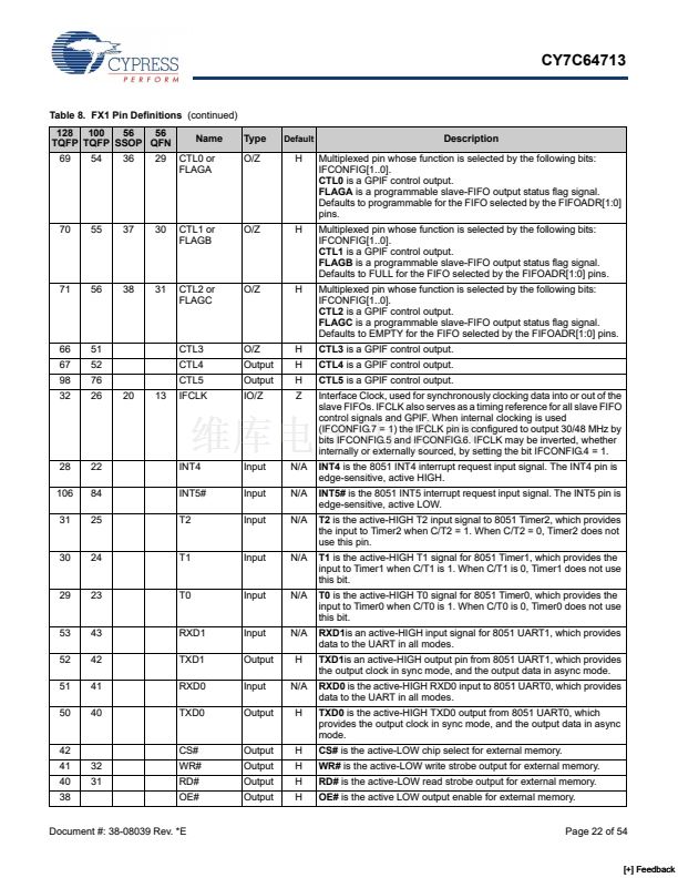
GPIF and FIFO Clock Rates
An 8051 register bit selects one of two frequencies for the
internally supplied interface clock: 30 MHz and 48 MHz. Alter-
natively, an externally supplied clock of 5 - 48 MHz feeding the
IFCLK pin is used as the interface clock. IFCLK is configured
to function as an output clock when the GPIF and FIFOs are
internally clocked. An output enable bit in the IFCONFIG
register turns this clock output off, if desired. Another bit within
the IFCONFIG register inverts the IFCLK signal whether inter-
nally or externally sourced.
what state a Ready input (or multiple inputs) must be before
proceeding. The GPIF vector is programmed to advance a
FIFO to the next data value, advance an address, and so on.
A sequence of the GPIF vectors create a single waveform that
executes to perform the data move between the FX1 and the
external device.
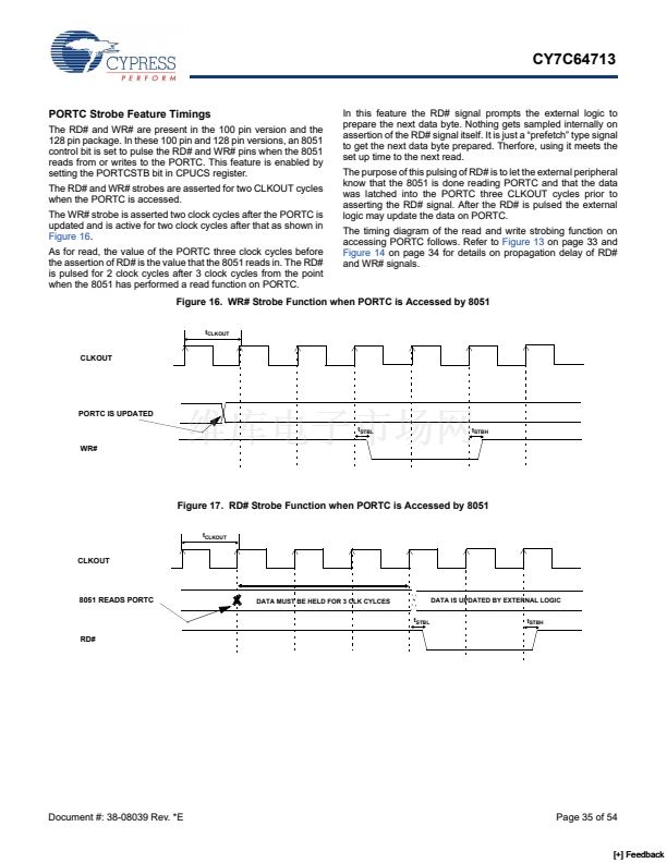
Six Control OUT Signals
The 100 and 128 pin packages bring out all six Control Output
pins (CTL0-CTL5). The 8051 programs the GPIF unit to define
the CTL waveforms. The 56 pin package brings out three of
these signals: CTL0 - CTL2. CTLx waveform edges are
programmed to make transitions as fast as once per clock
(20.8 ns using a 48 MHz clock).
Six Ready IN Signals
The 100 and 128 pin packages bring out all six Ready inputs
(RDY0鈥揜DY5). The 8051 programs the GPIF unit to test the
RDY pins for GPIF branching. The 56 pin package brings out
two of these signals, RDY0鈥?.
Nine GPIF Address OUT Signals
Nine GPIF address lines are available in the 100 and 128 pin
packages: GPIFADR[8..0]. The GPIF address lines allow
indexing through up to a 512 byte block of RAM. If more
address lines are needed, IO port pins are used.
Long Transfer Mode
In Master mode, the 8051 appropriately sets the GPIF trans-
action count registers (GPIFTCB3, GPIFTCB2, GPIFTCB1, or
GPIFTCB0) for unattended transfers of up to 2
32
transactions.
The GPIF automatically throttles data flow to prevent under or
overflow until the full number of requested transactions are
complete. The GPIF decrements the value in these registers
to represent the current status of the transaction.
ECC Generation
The EZ-USB FX1 can calculate ECCs (Error Correcting
Codes) on data that pass across its GPIF or Slave FIFO inter-
faces. There are two ECC configurations: Two ECCs, each
calculated over 256 bytes (SmartMedia鈩?Standard); and one
ECC calculated over 512 bytes.
The ECC can correct any one-bit error or detect any two-bit
error.
Note
To use the ECC logic, the GPIF or Slave FIFO interface
must be configured for byte-wide operation.
ECC Implementation
The two ECC configurations are selected by the ECCM bit:
0.0.0.1 ECCM = 0
Two 3-byte ECCs, each calculated over a 256-byte block of
data. This configuration conforms to the SmartMedia
Standard.
Write any value to ECCRESET, then pass data across the
GPIF or Slave FIFO interface. The ECC for the first 256 bytes
of data is calculated and stored in ECC1. The ECC for the next
256 bytes is stored in ECC2. After the second ECC is calcu-
lated, the values in the ECCx registers do not change until the
ECCRESET is written again, even if more data is subse-
quently passed across the interface.
GPIF
The GPIF is a flexible 8 or 16-bit parallel interface driven by a
user programmable finite state machine. It allows the
CY7C64713 to perform local bus mastering, and can
implement a wide variety of protocols such as ATA interface,
printer parallel port, and Utopia.
The GPIF has six programmable control outputs (CTL), nine
address outputs (GPIFADRx), and six general purpose Ready
inputs (RDY). The data bus width is 8 or 16 bits. Each GPIF
vector defines the state of the control outputs, and determines
Document #: 38-08039 Rev. *E
Page 10 of 54
[+] Feedback


 1
1
 2
2
 3
3
 4
4
 5
5
 6
6
 7
7
 8
8
 9
9
 10
10
 11
11
 12
12
 13
13
 14
14
 15
15
 16
16
 17
17
 18
18
 19
19
 20
20
 21
21
 22
22
 23
23
 24
24
 25
25
 26
26
 27
27
 28
28
 29
29
 30
30
 31
31
 32
32
 33
33
 34
34
 35
35
 36
36
 37
37
 38
38
 39
39
 40
40
 41
41
 42
42
 43
43
 44
44
 45
45
 46
46
 47
47
 48
48
 49
49
 50
50
 51
51
 52
52
 53
53
 54
54
