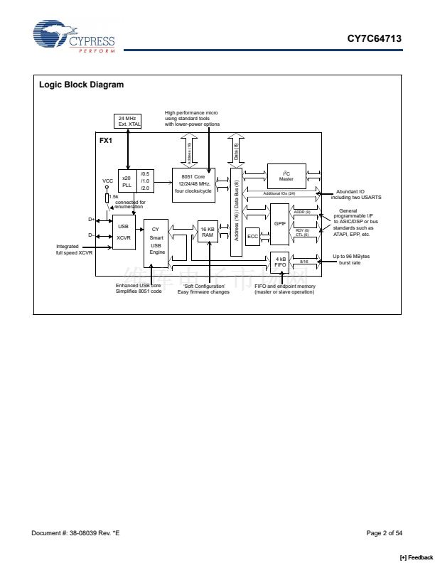
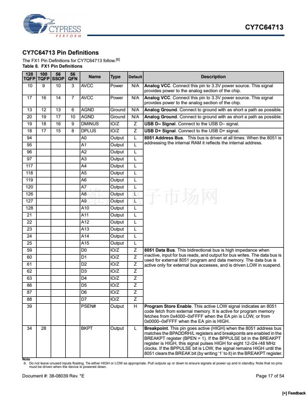
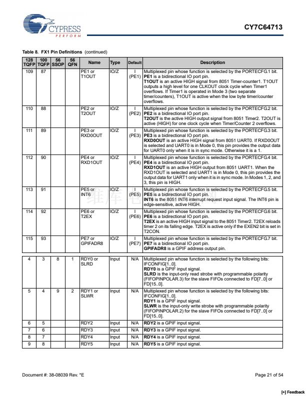
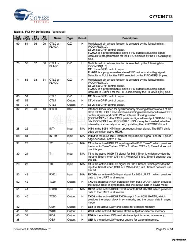
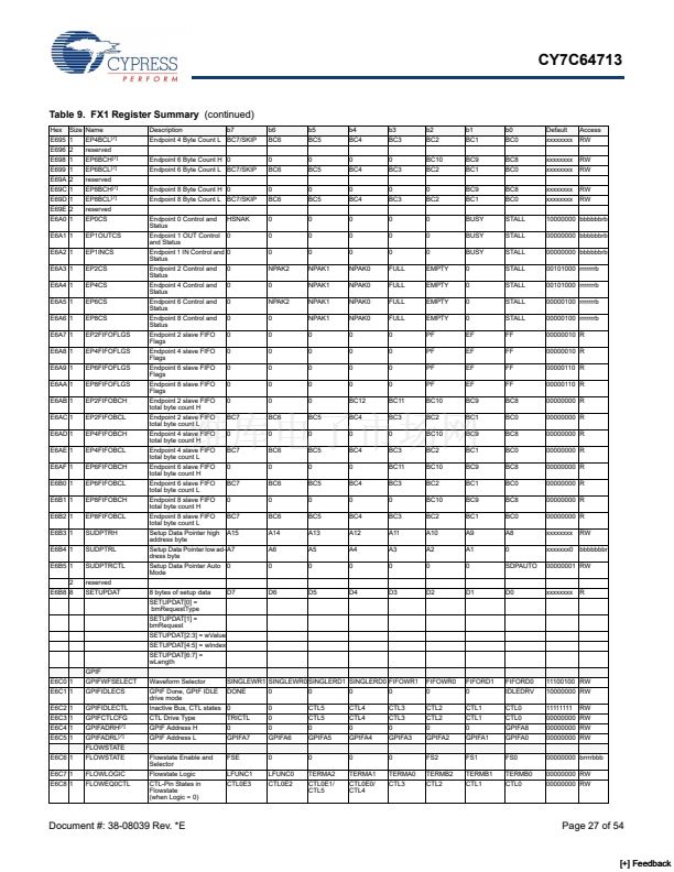
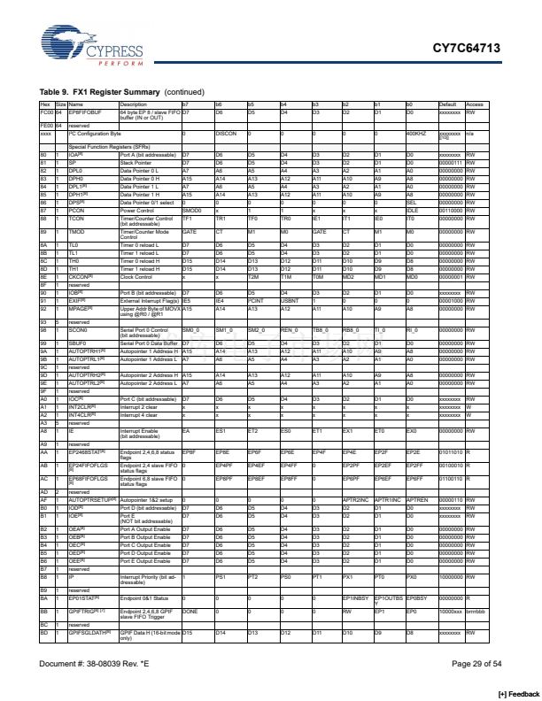
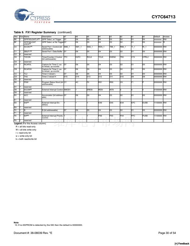
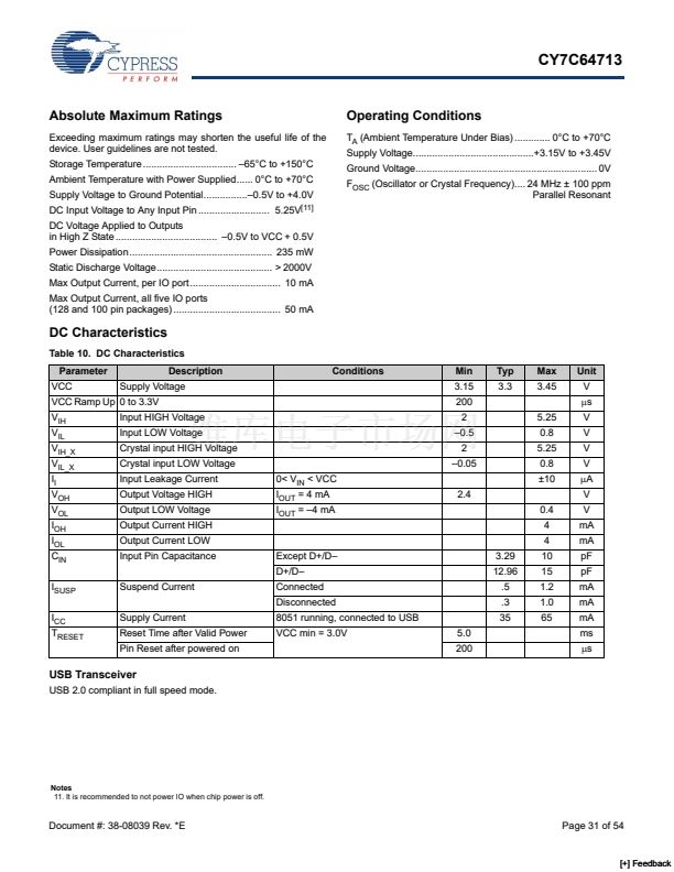
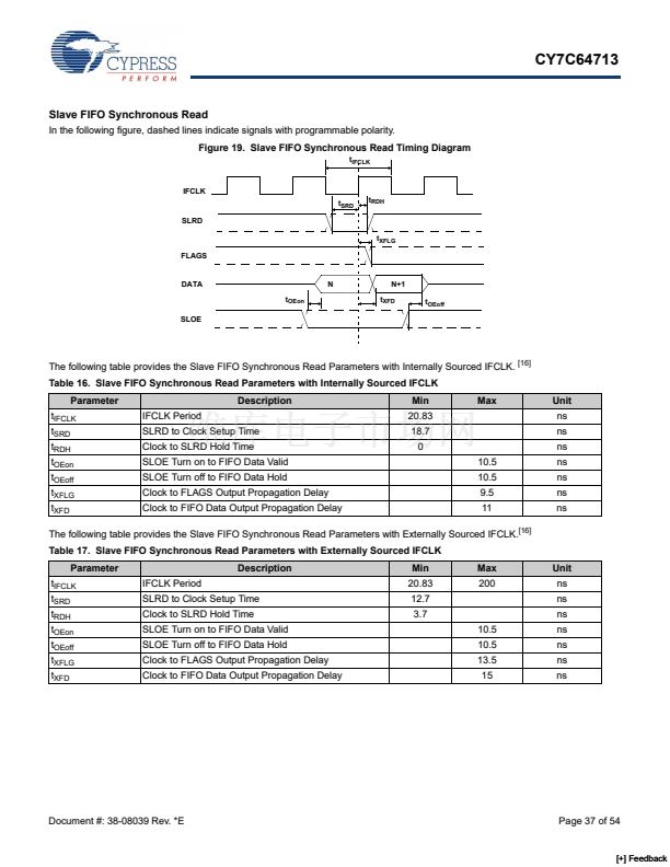
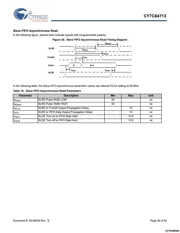
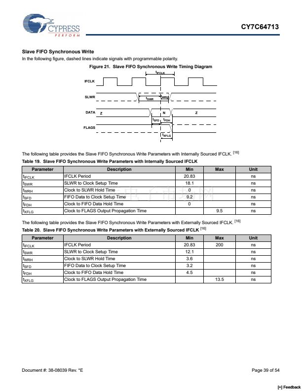
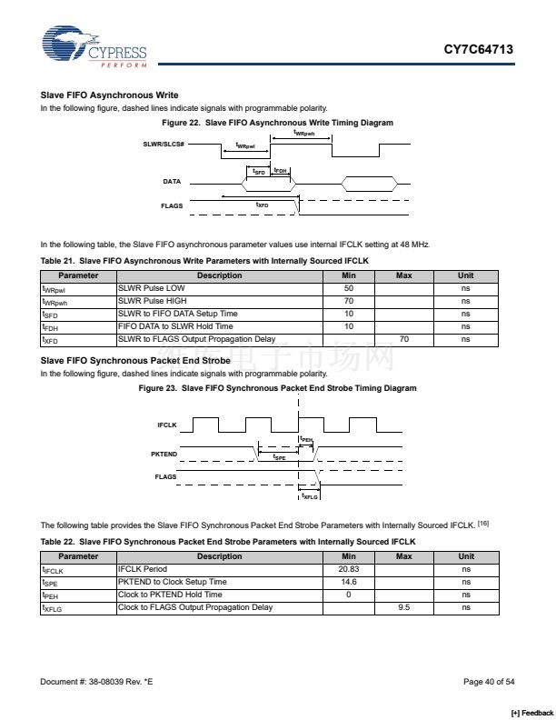
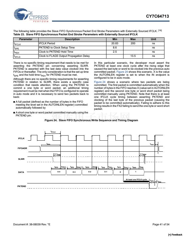
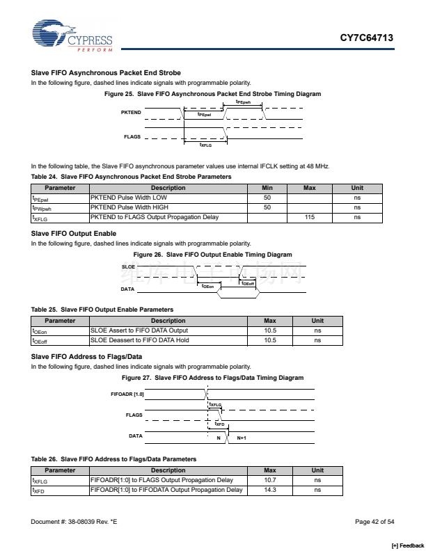
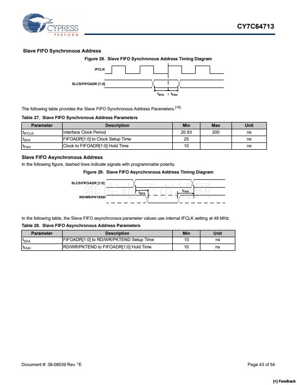
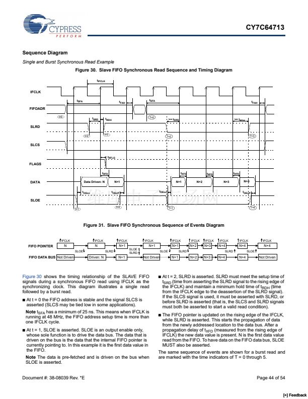
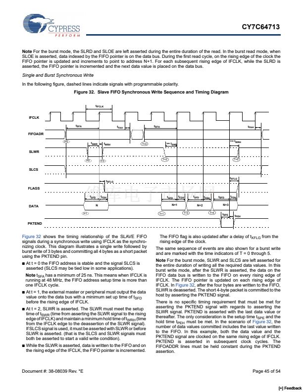
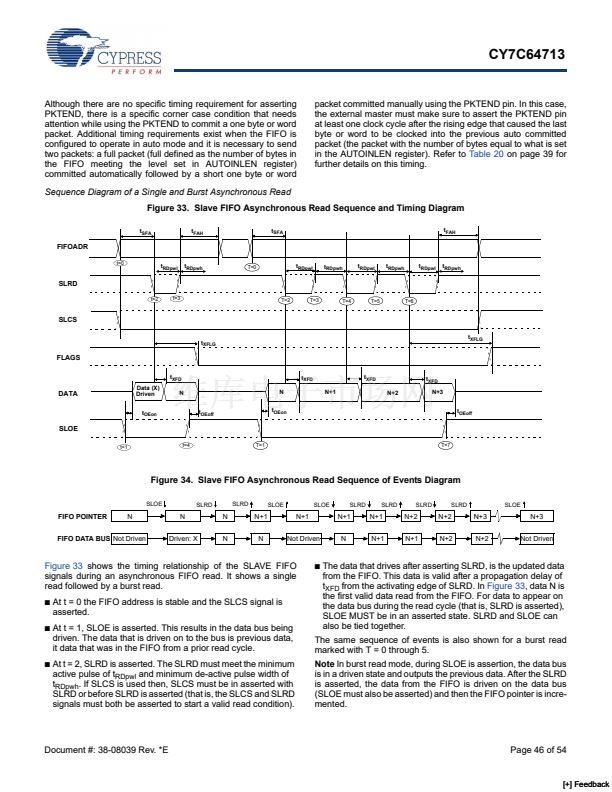
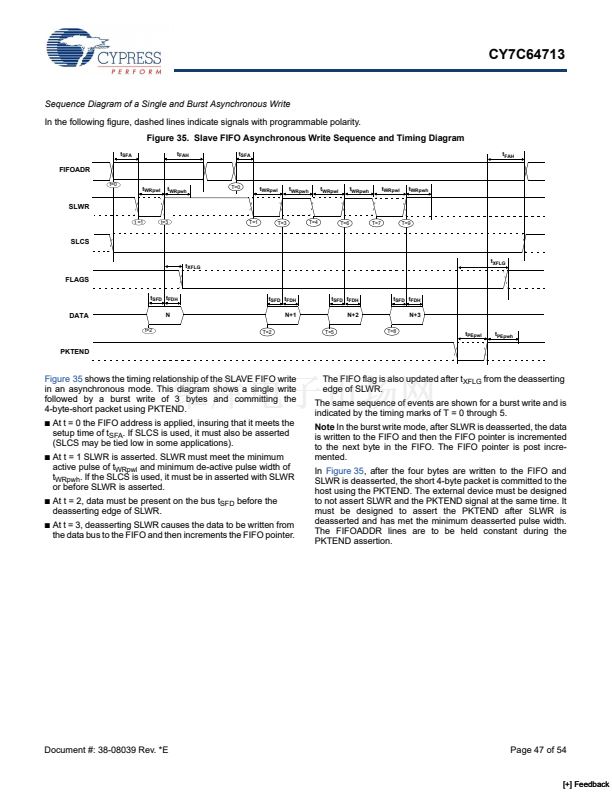
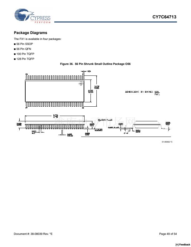
CY7C64713
CY7C64713 Pin Definitions
The FX1 Pin Definitions for CY7C64713 follow.
[6]
Table 8. FX1 Pin Definitions
128 100
56
56
TQFP TQFP SSOP QFN
10
17
13
20
19
18
94
95
96
97
117
118
119
120
126
127
128
21
22
23
24
25
59
60
61
62
63
86
87
88
39
9
16
12
19
18
17
10
14
13
17
16
15
3
7
6
10
9
8
Name
AVCC
AVCC
AGND
AGND
DMINUS
DPLUS
A0
A1
A2
A3
A4
A5
A6
A7
A8
A9
A10
A11
A12
A13
A14
A15
D0
D1
D2
D3
D4
D5
D6
D7
PSEN#
Type
Power
Power
Ground
Ground
IO/Z
IO/Z
Output
Output
Output
Output
Output
Output
Output
Output
Output
Output
Output
Output
Output
Output
Output
Output
IO/Z
IO/Z
IO/Z
IO/Z
IO/Z
IO/Z
IO/Z
IO/Z
Output
Default
Description
Analog VCC.
Connect this pin to 3.3V power source. This signal
provides power to the analog section of the chip.
Analog VCC.
Connect this pin to 3.3V power source. This signal
provides power to the analog section of the chip.
Analog Ground.
Connect to ground with as short a path as possible.
Analog Ground.
Connect to ground with as short a path as possible.
USB D鈥?Signal.
Connect to the USB D鈥?signal.
USB D+ Signal.
Connect to the USB D+ signal.
8051 Address Bus.
This bus is driven at all times. When the 8051 is
addressing the internal RAM it reflects the internal address.
N/A
N/A
N/A
N/A
Z
Z
L
L
L
L
L
L
L
L
L
L
L
L
L
L
L
L
Z
Z
Z
Z
Z
Z
Z
Z
H
8051 Data Bus.
This bidirectional bus is high impedance when
inactive, input for bus reads, and output for bus writes. The data bus is
used for external 8051 program and data memory. The data bus is
active only for external bus accesses, and is driven LOW in suspend.
Program Store Enable.
This active LOW signal indicates an 8051
code fetch from external memory. It is active for program memory
fetches from 0x4000鈥?xFFFF when the EA pin is LOW, or from
0x0000鈥?xFFFF when the EA pin is HIGH.
Breakpoint.
This pin goes active (HIGH) when the 8051 address bus
matches the BPADDRH/L registers and breakpoints are enabled in the
BREAKPT register (BPEN = 1). If the BPPULSE bit in the BREAKPT
register is HIGH, this signal pulses HIGH for eight 12-/24-/48 MHz
clocks. If the BPPULSE bit is LOW, the signal remains HIGH until the
8051 clears the BREAK bit (by writing 鈥?鈥?to it) in the BREAKPT register.
34
28
BKPT
Output
L
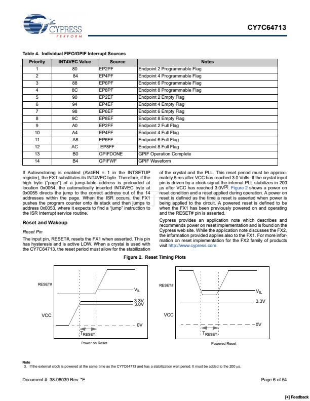
Note
6. Do not leave unused inputs floating. Tie either HIGH or LOW as appropriate. Pull outputs up or down to ensure signals at power up and in standby. Note that no pins
must be driven when the device is powered down.
Document #: 38-08039 Rev. *E
Page 17 of 54
[+] Feedback


 1
1
 2
2
 3
3
 4
4
 5
5
 6
6
 7
7
 8
8
 9
9
 10
10
 11
11
 12
12
 13
13
 14
14
 15
15
 16
16
 17
17
 18
18
 19
19
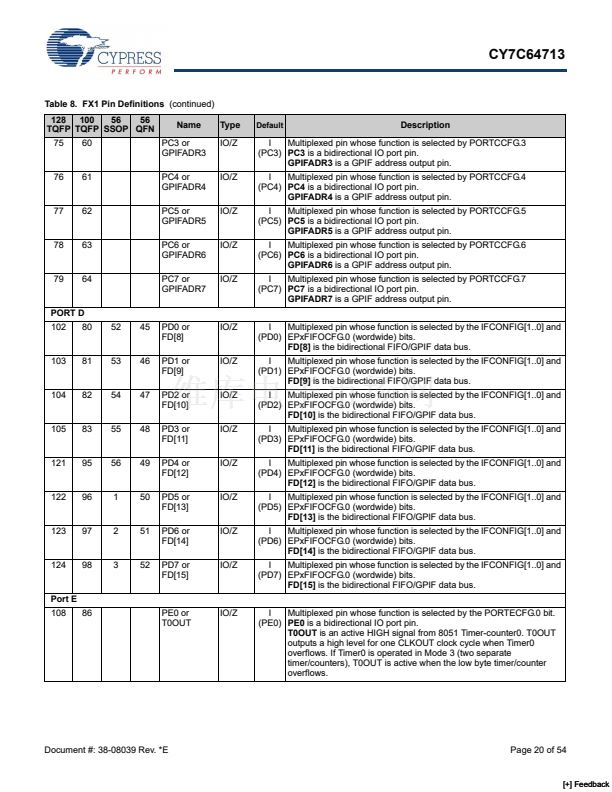 20
20
 21
21
 22
22
 23
23
 24
24
 25
25
 26
26
 27
27
 28
28
 29
29
 30
30
 31
31
 32
32
 33
33
 34
34
 35
35
 36
36
 37
37
 38
38
 39
39
 40
40
 41
41
 42
42
 43
43
 44
44
 45
45
 46
46
 47
47
 48
48
 49
49
 50
50
 51
51
 52
52
 53
53
 54
54
