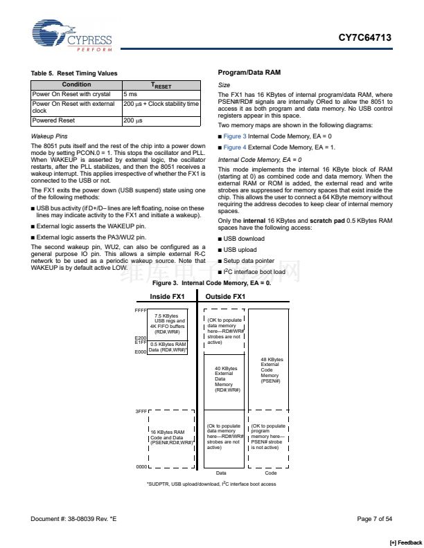
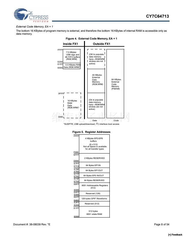
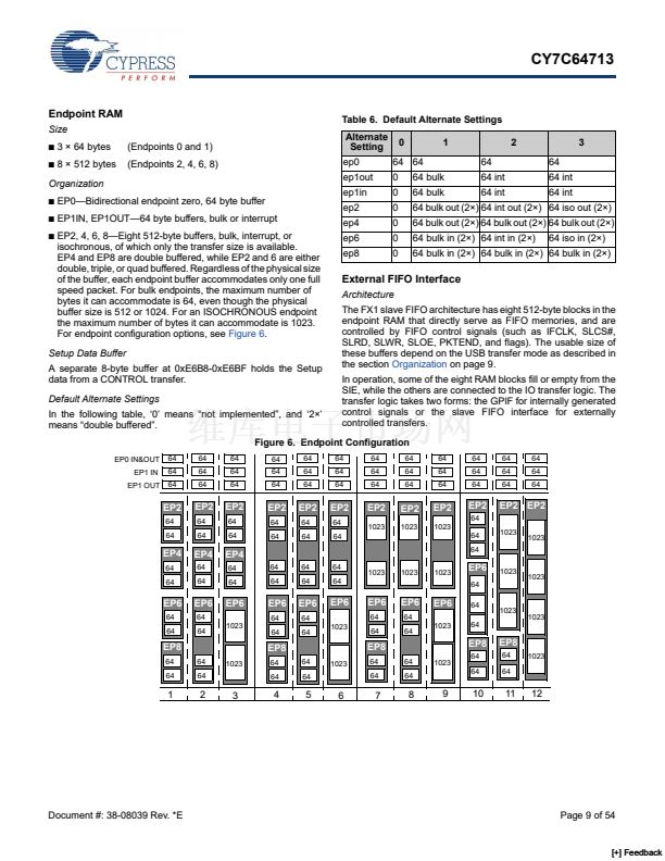
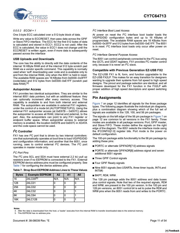
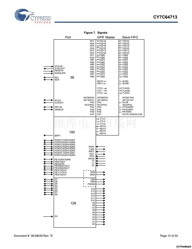
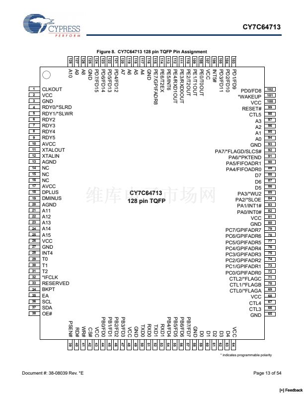
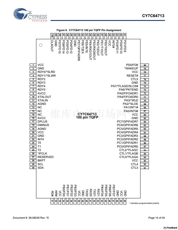
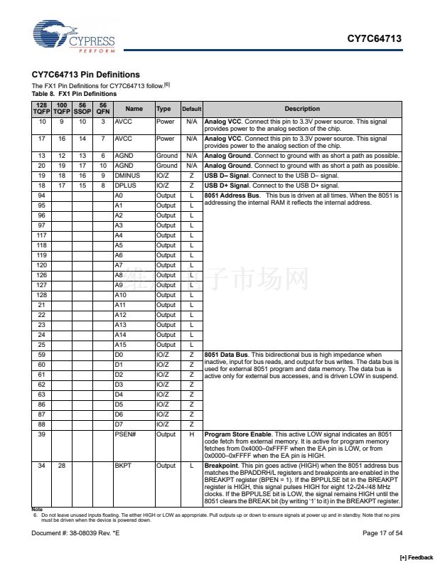
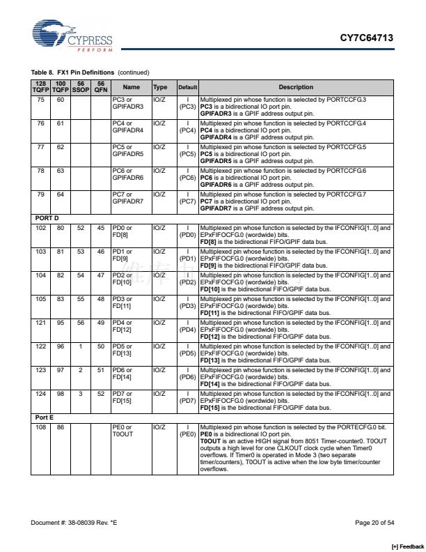
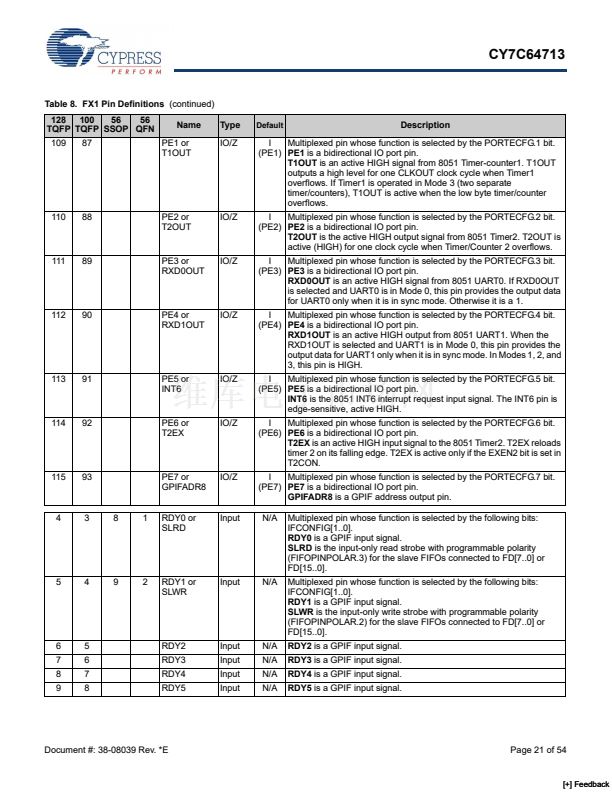
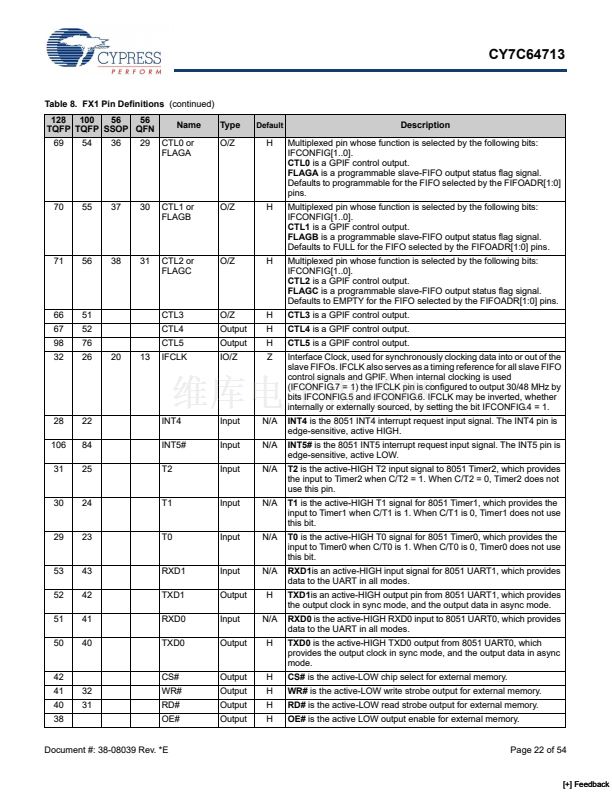
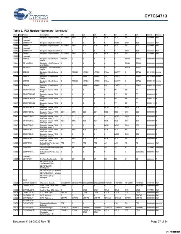
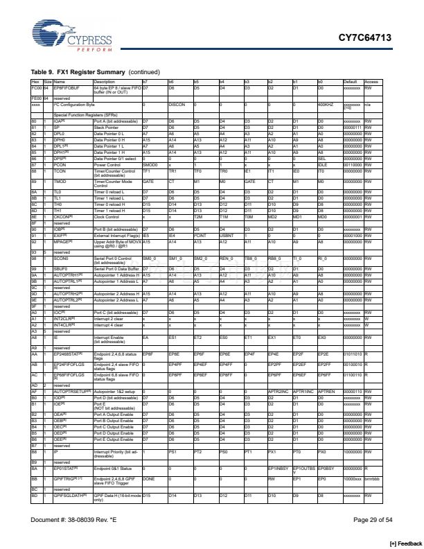
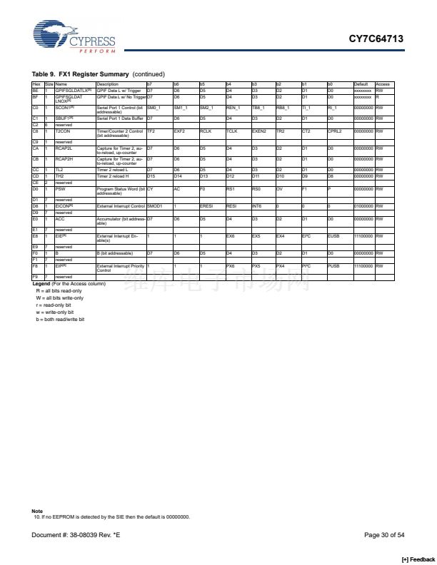
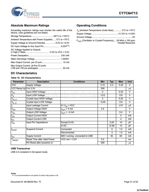
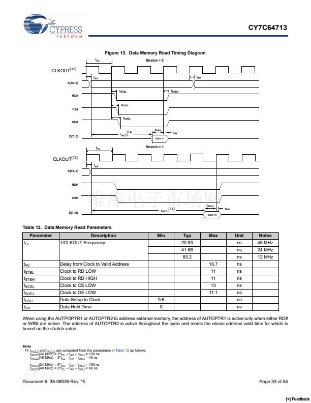
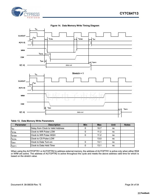
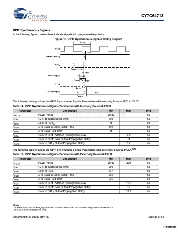
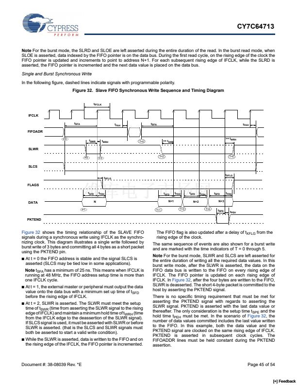
CY7C64713
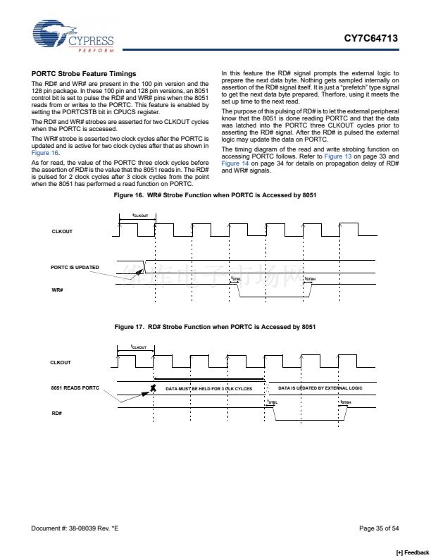
PORTC Strobe Feature Timings
The RD# and WR# are present in the 100 pin version and the
128 pin package. In these 100 pin and 128 pin versions, an 8051
control bit is set to pulse the RD# and WR# pins when the 8051
reads from or writes to the PORTC. This feature is enabled by
setting the PORTCSTB bit in CPUCS register.
The RD# and WR# strobes are asserted for two CLKOUT cycles
when the PORTC is accessed.
The WR# strobe is asserted two clock cycles after the PORTC is
updated and is active for two clock cycles after that as shown in
Figure 16.
As for read, the value of the PORTC three clock cycles before
the assertion of RD# is the value that the 8051 reads in. The RD#
is pulsed for 2 clock cycles after 3 clock cycles from the point
when the 8051 has performed a read function on PORTC.
In this feature the RD# signal prompts the external logic to
prepare the next data byte. Nothing gets sampled internally on
assertion of the RD# signal itself. It is just a 鈥減refetch鈥?type signal
to get the next data byte prepared. Therfore, using it meets the
set up time to the next read.
The purpose of this pulsing of RD# is to let the external peripheral
know that the 8051 is done reading PORTC and that the data
was latched into the PORTC three CLKOUT cycles prior to
asserting the RD# signal. After the RD# is pulsed the external
logic may update the data on PORTC.
The timing diagram of the read and write strobing function on
accessing PORTC follows. Refer to
Figure 13
on page 33 and
Figure 14
on page 34 for details on propagation delay of RD#
and WR# signals.
Figure 16. WR# Strobe Function when PORTC is Accessed by 8051
t
CLKOUT
CLKOUT
PORTC IS UPDATED
t
STBL
t
STBH
WR#
Figure 17. RD# Strobe Function when PORTC is Accessed by 8051
t
CLKOUT
CLKOUT
8051 READS PORTC
DATA MUST BE HELD FOR 3 CLK CYLCES
t
STBL
DATA IS UPDATED BY EXTERNAL LOGIC
t
STBH
RD#
Document #: 38-08039 Rev. *E
Page 35 of 54
[+] Feedback


 1
1
 2
2
 3
3
 4
4
 5
5
 6
6
 7
7
 8
8
 9
9
 10
10
 11
11
 12
12
 13
13
 14
14
 15
15
 16
16
 17
17
 18
18
 19
19
 20
20
 21
21
 22
22
 23
23
 24
24
 25
25
 26
26
 27
27
 28
28
 29
29
 30
30
 31
31
 32
32
 33
33
 34
34
 35
35
 36
36
 37
37
 38
38
 39
39
 40
40
 41
41
 42
42
 43
43
 44
44
 45
45
 46
46
 47
47
 48
48
 49
49
 50
50
 51
51
 52
52
 53
53
 54
54
