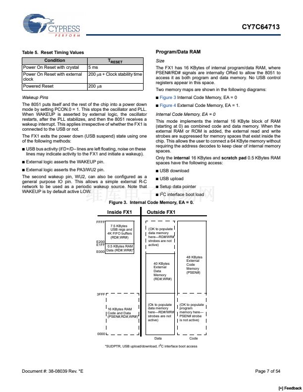
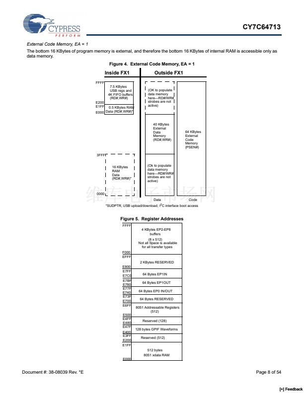
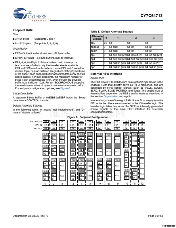
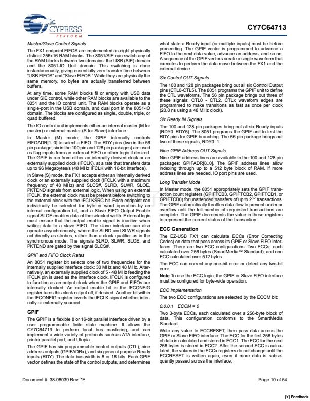
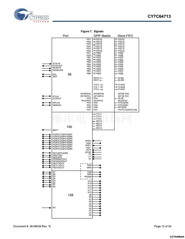
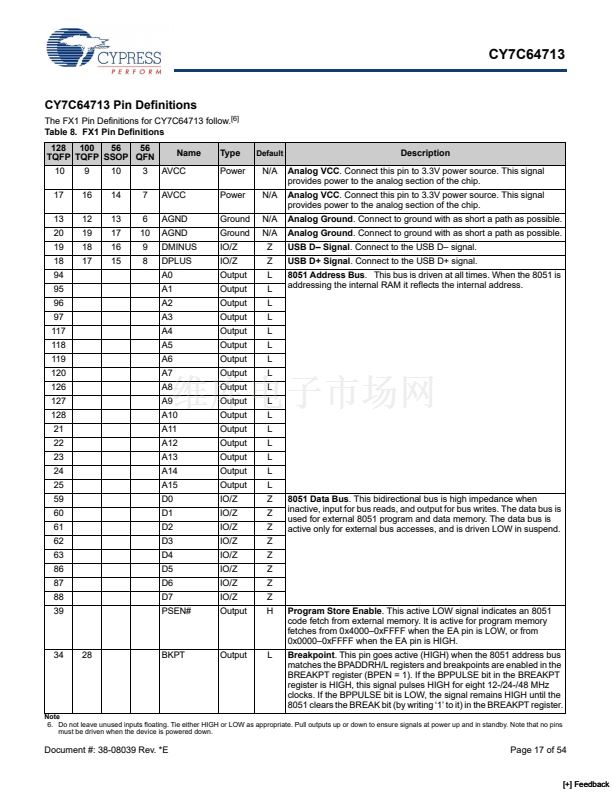
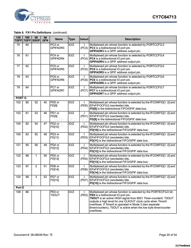
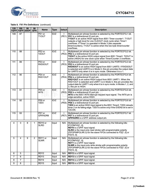
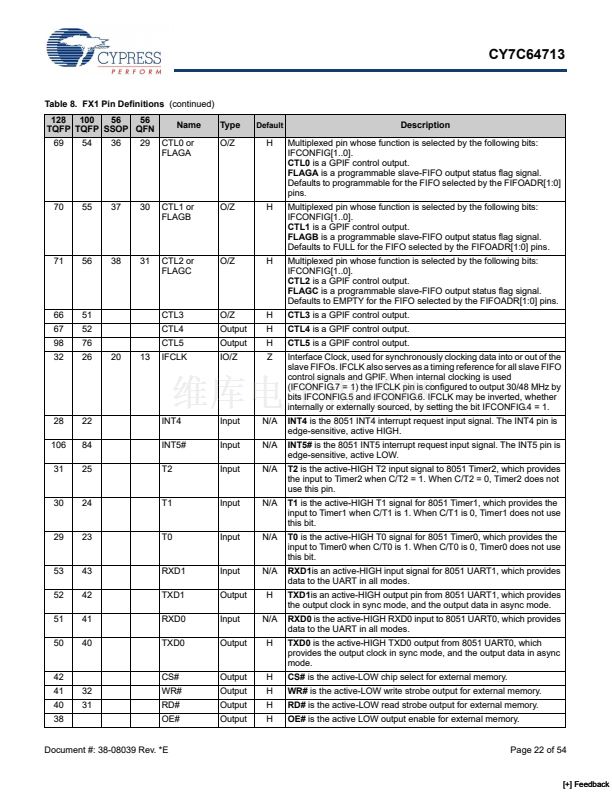
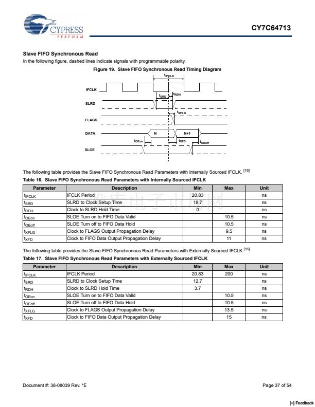
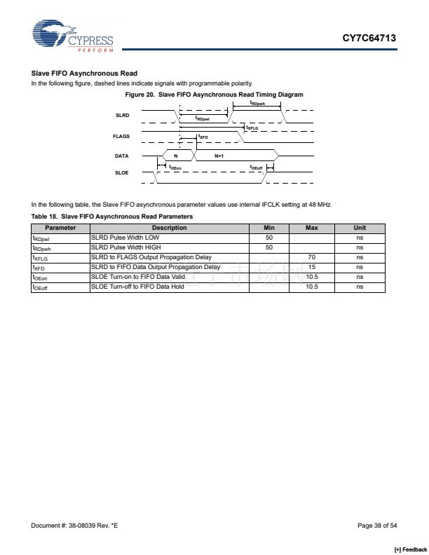
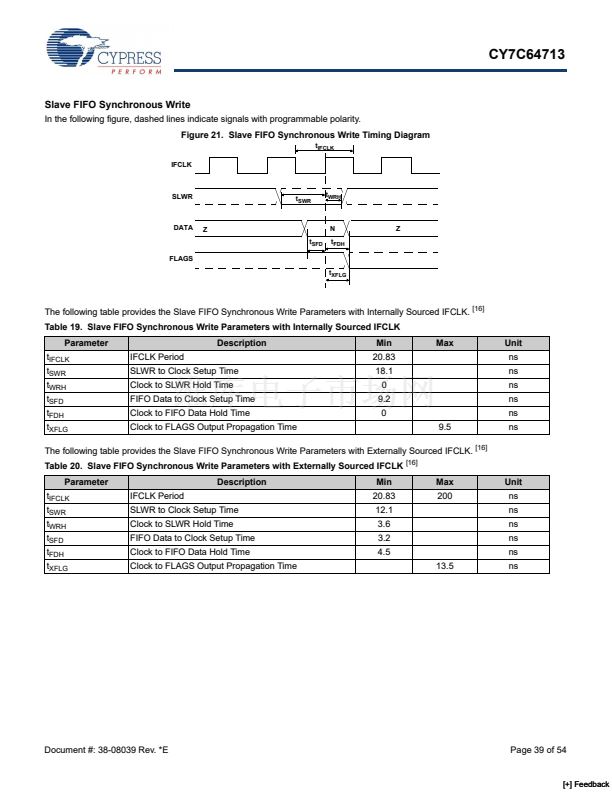
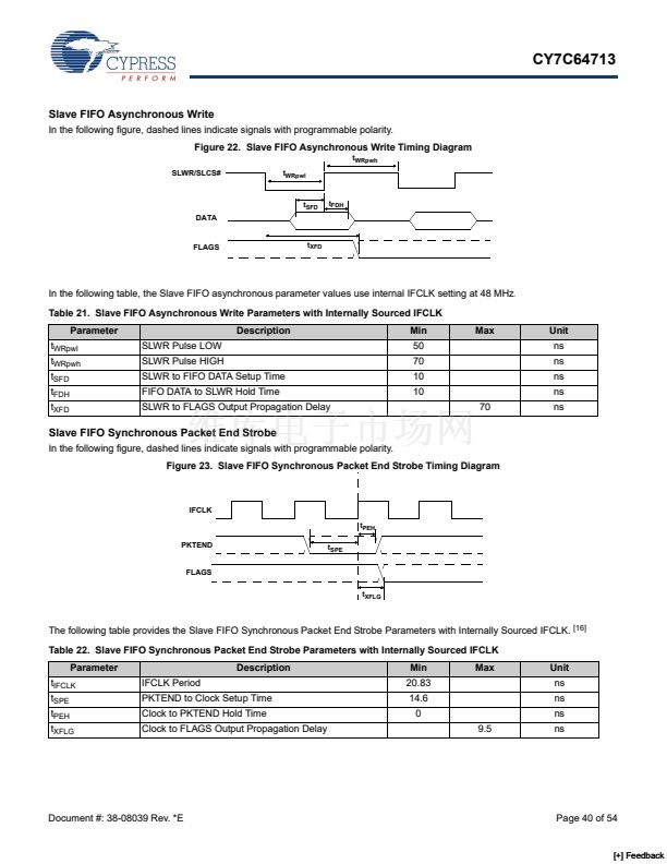
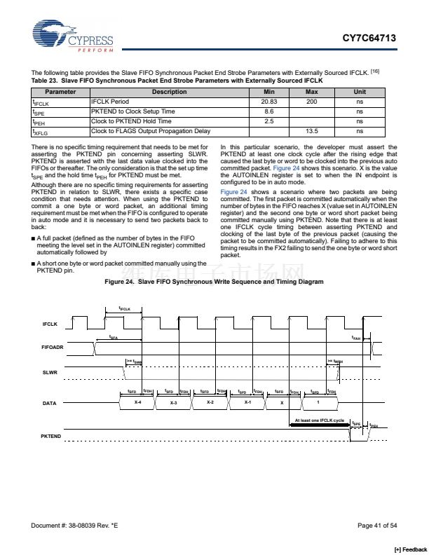
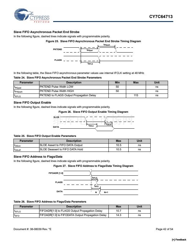
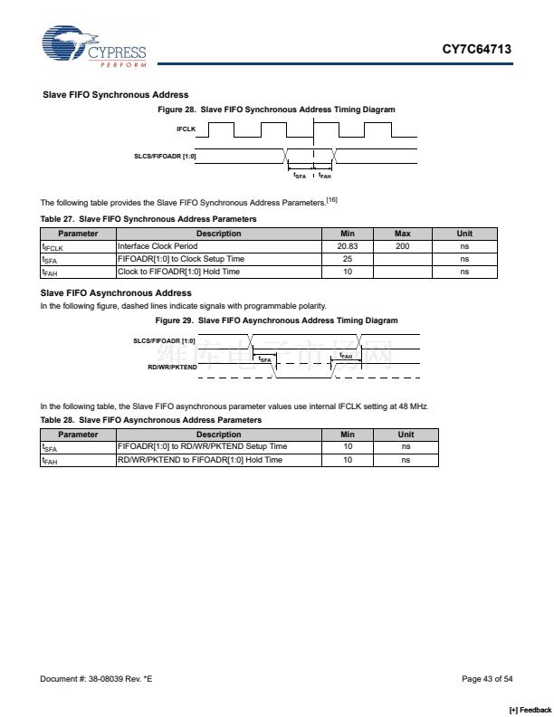
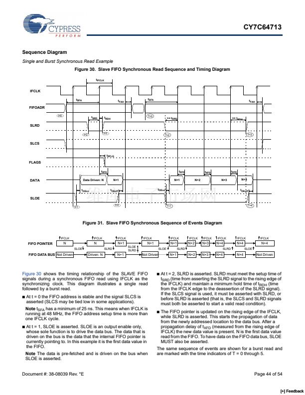
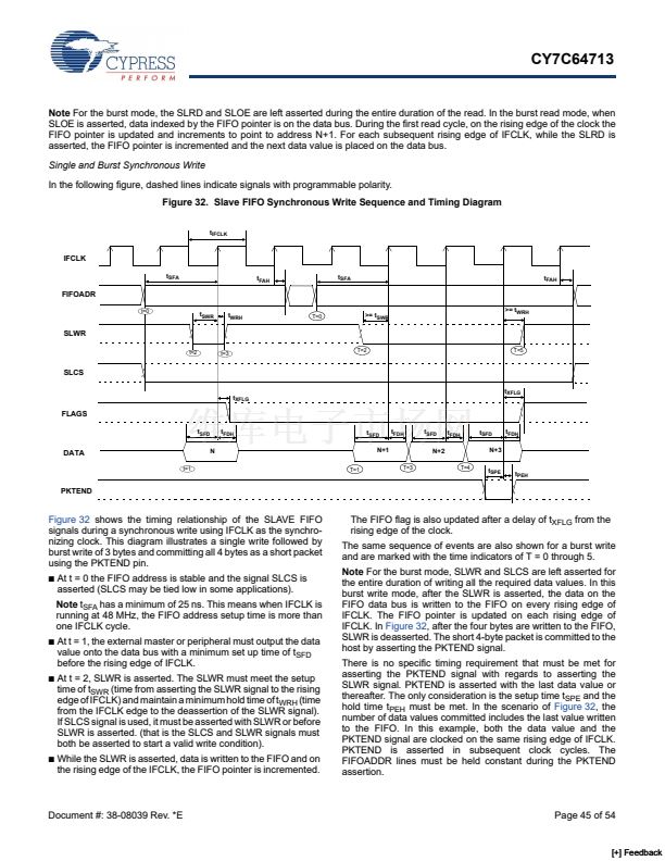
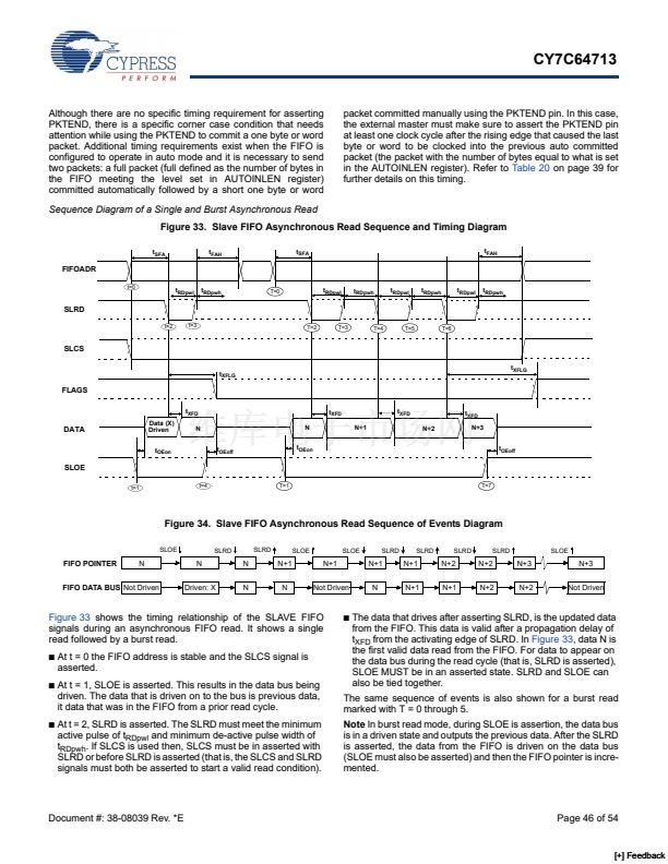
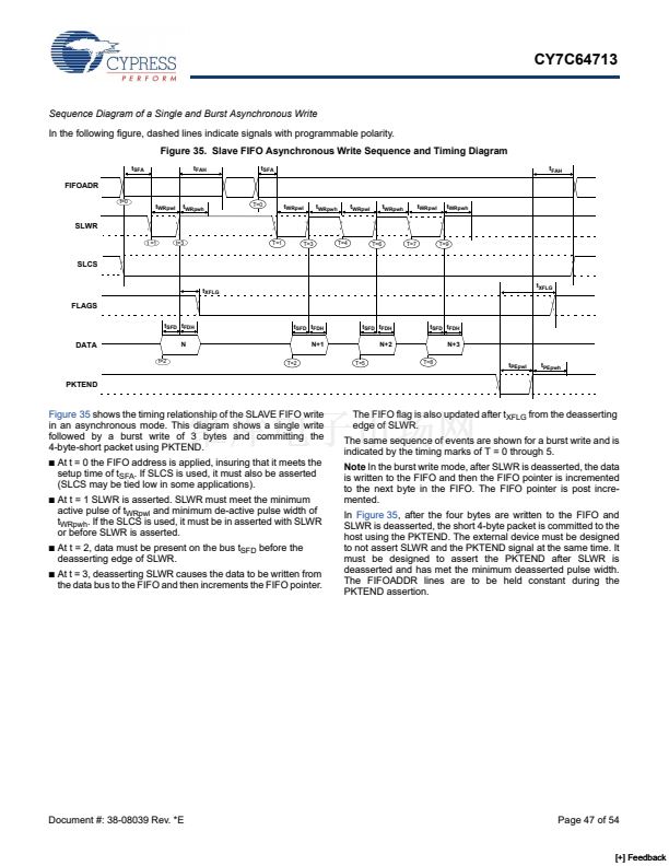
In the following figure, dashed lines indicate signals with programmable polarity.
Figure 35. Slave FIFO Asynchronous Write Sequence and Timing Diagram
in an asynchronous mode. This diagram shows a single write
4-byte-short packet using PKTEND.
鈻?/div>
The FIFO flag is also updated after t
XFLG
from the deasserting
edge of SLWR.
The same sequence of events are shown for a burst write and is
indicated by the timing marks of T = 0 through 5.
Note
In the burst write mode, after SLWR is deasserted, the data
is written to the FIFO and then the FIFO pointer is incremented
to the next byte in the FIFO. The FIFO pointer is post incre-
mented.
In
Figure 35,
after the four bytes are written to the FIFO and
SLWR is deasserted, the short 4-byte packet is committed to the
host using the PKTEND. The external device must be designed
to not assert SLWR and the PKTEND signal at the same time. It
must be designed to assert the PKTEND after SLWR is
deasserted and has met the minimum deasserted pulse width.
The FIFOADDR lines are to be held constant during the
PKTEND assertion.
At t = 0 the FIFO address is applied, insuring that it meets the
setup time of t
SFA
. If SLCS is used, it must also be asserted
(SLCS may be tied low in some applications).
At t = 1 SLWR is asserted. SLWR must meet the minimum
active pulse of t
WRpwl
and minimum de-active pulse width of
t
WRpwh
. If the SLCS is used, it must be in asserted with SLWR
or before SLWR is asserted.
At t = 2, data must be present on the bus t
SFD
before the
deasserting edge of SLWR.
At t = 3, deasserting SLWR causes the data to be written from
the data bus to the FIFO and then increments the FIFO pointer.
鈻?/div>
鈻?/div>
鈻?/div>
Document #: 38-08039 Rev. *E
Page 47 of 54
[+] Feedback


 1
1
 2
2
 3
3
 4
4
 5
5
 6
6
 7
7
 8
8
 9
9
 10
10
 11
11
 12
12
 13
13
 14
14
 15
15
 16
16
 17
17
 18
18
 19
19
 20
20
 21
21
 22
22
 23
23
 24
24
 25
25
 26
26
 27
27
 28
28
 29
29
 30
30
 31
31
 32
32
 33
33
 34
34
 35
35
 36
36
 37
37
 38
38
 39
39
 40
40
 41
41
 42
42
 43
43
 44
44
 45
45
 46
46
 47
47
 48
48
 49
49
 50
50
 51
51
 52
52
 53
53
 54
54
