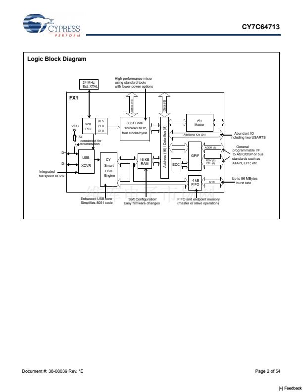
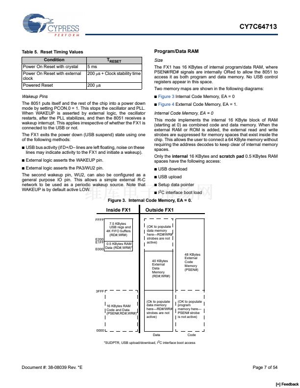
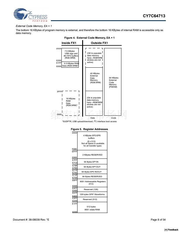
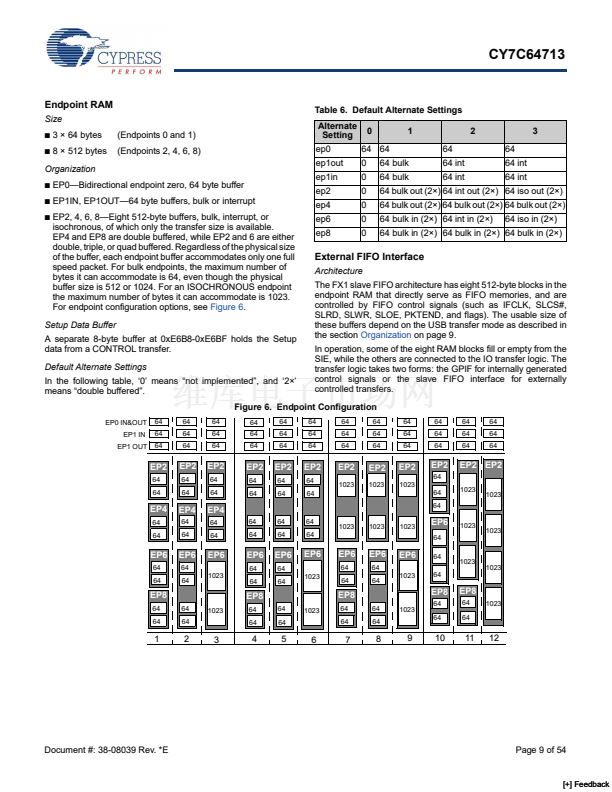
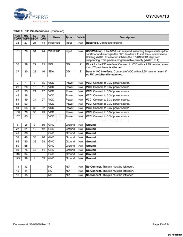
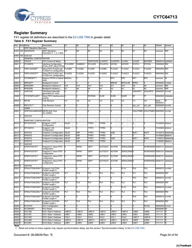
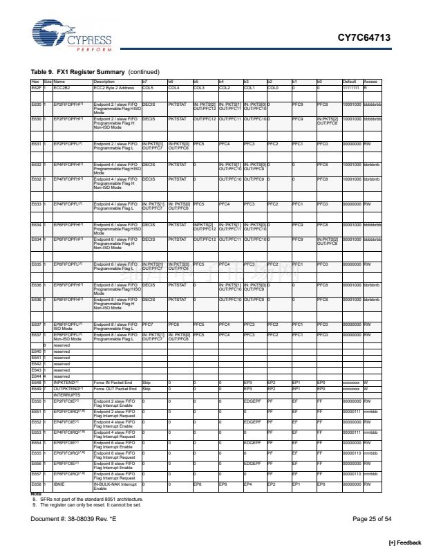
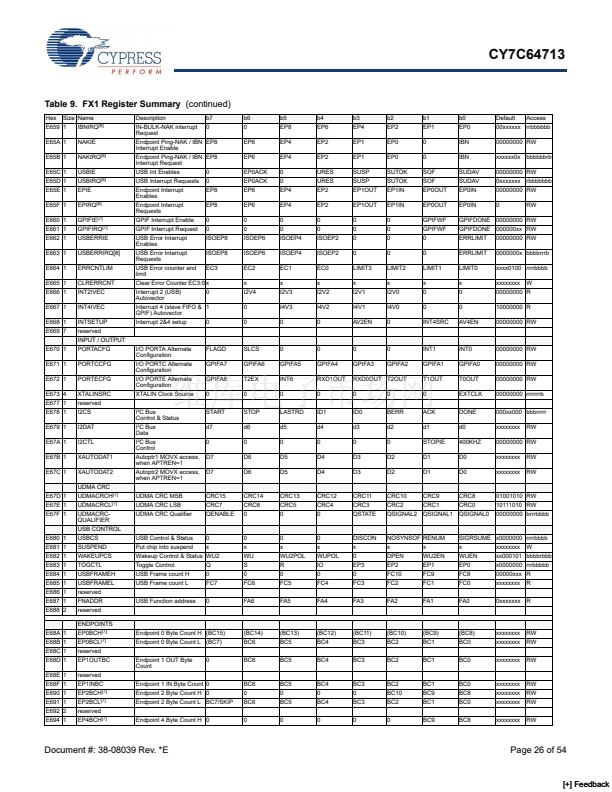
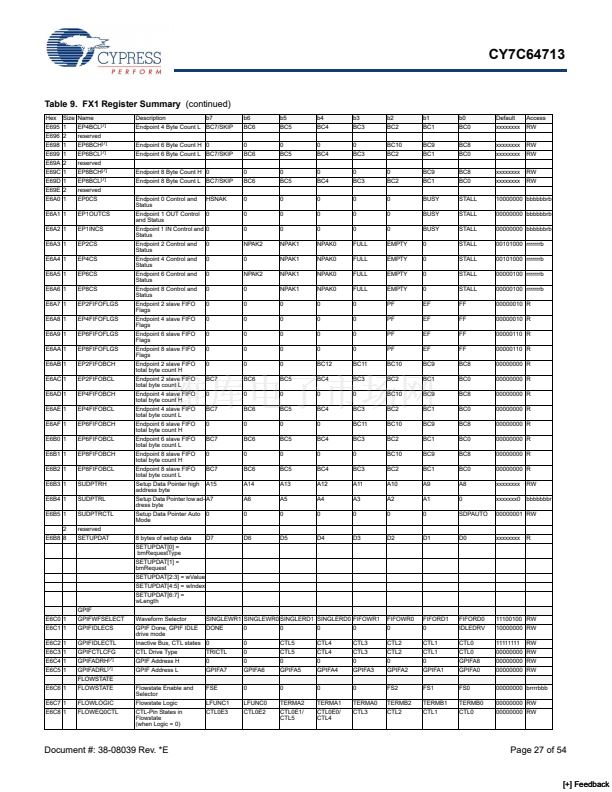
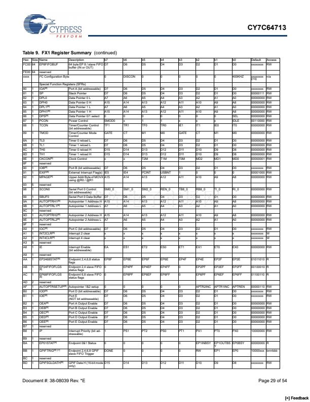
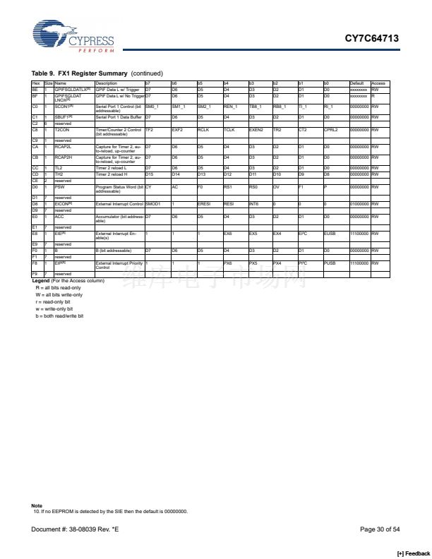
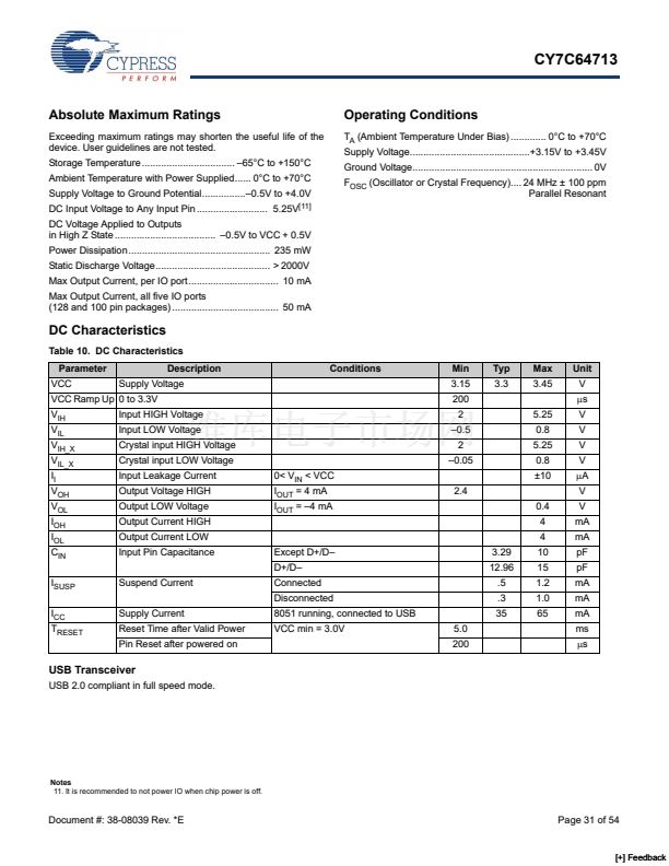
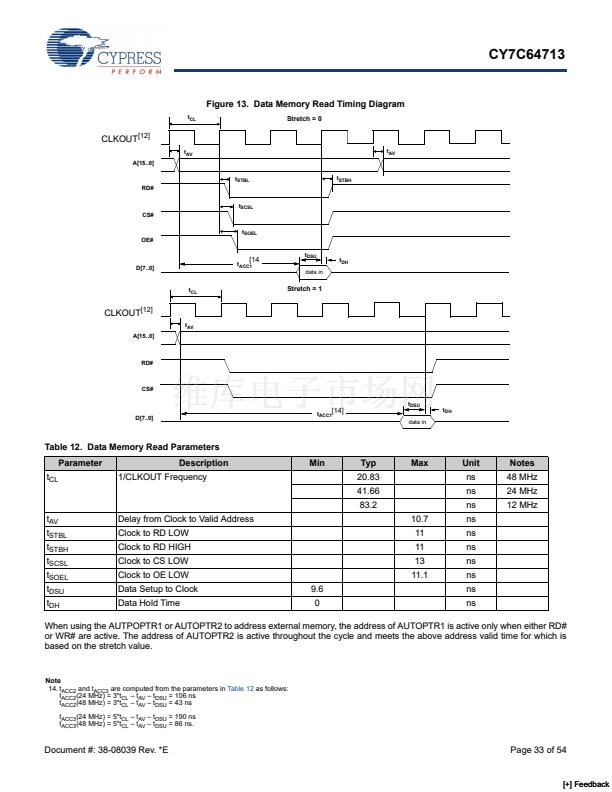
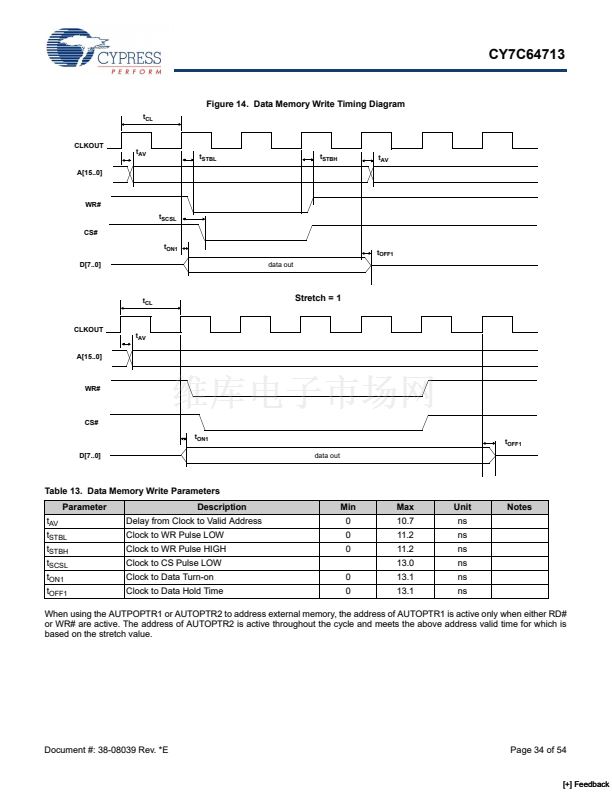
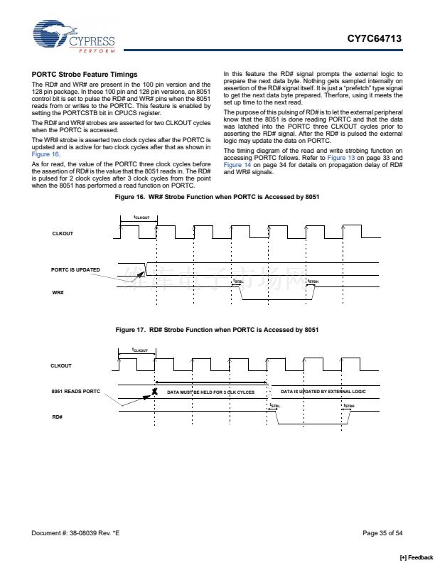
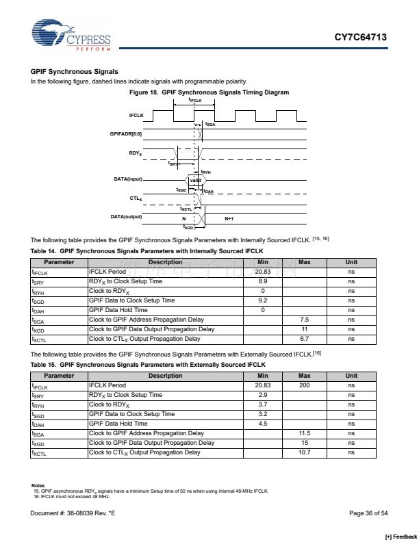
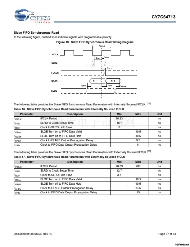
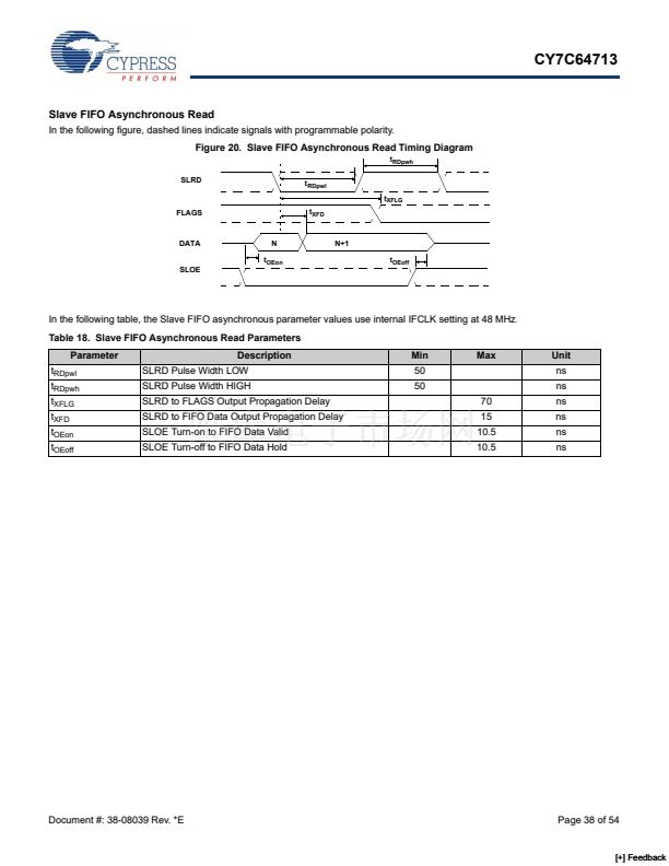
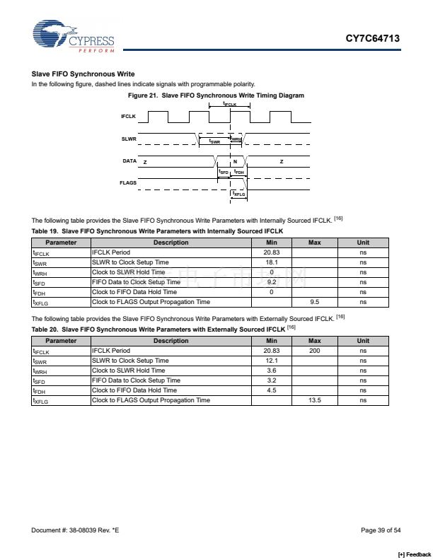
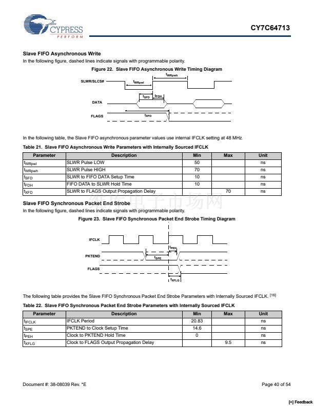
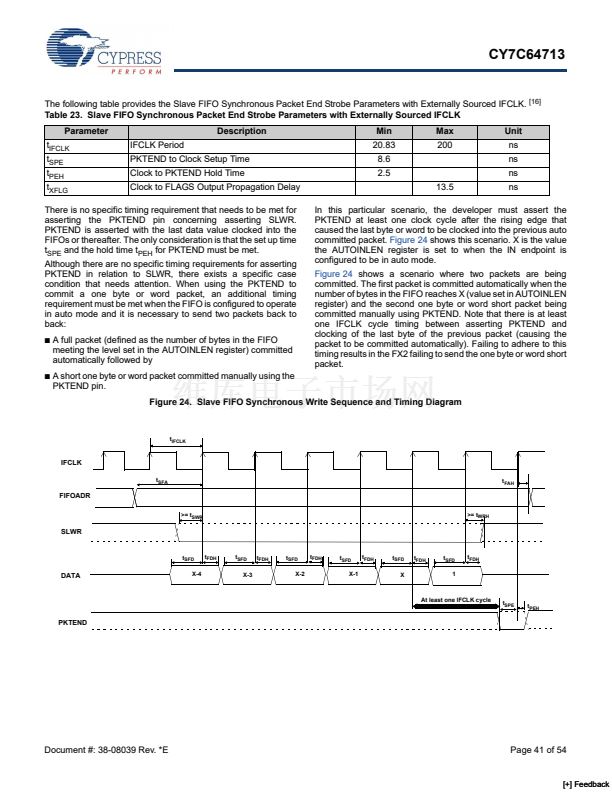
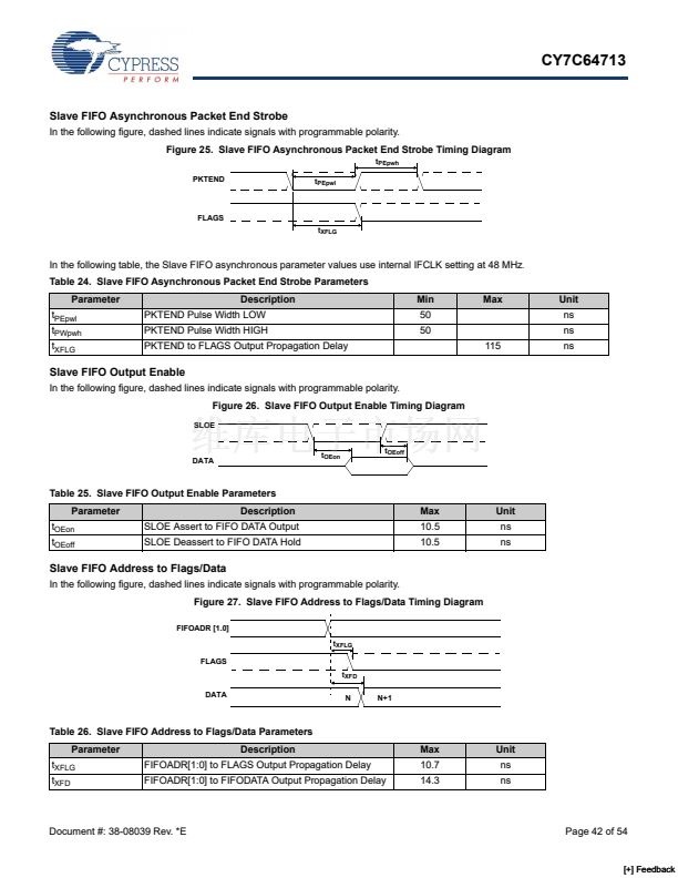
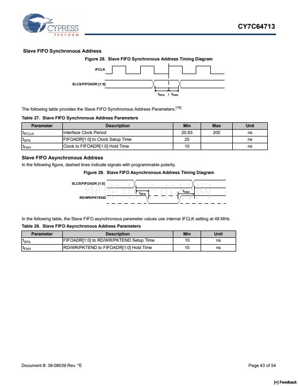
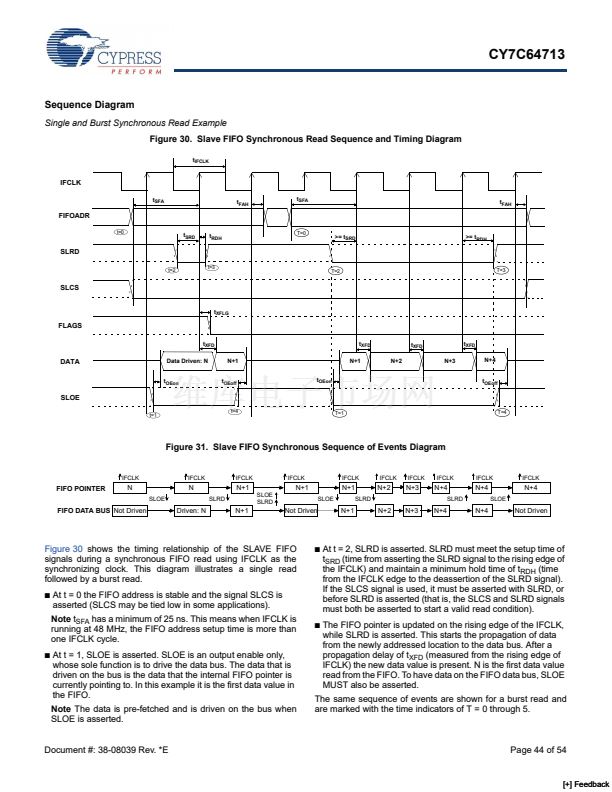
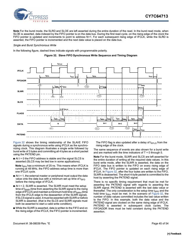
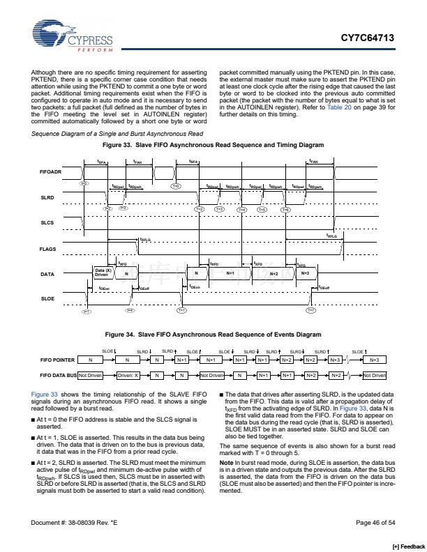
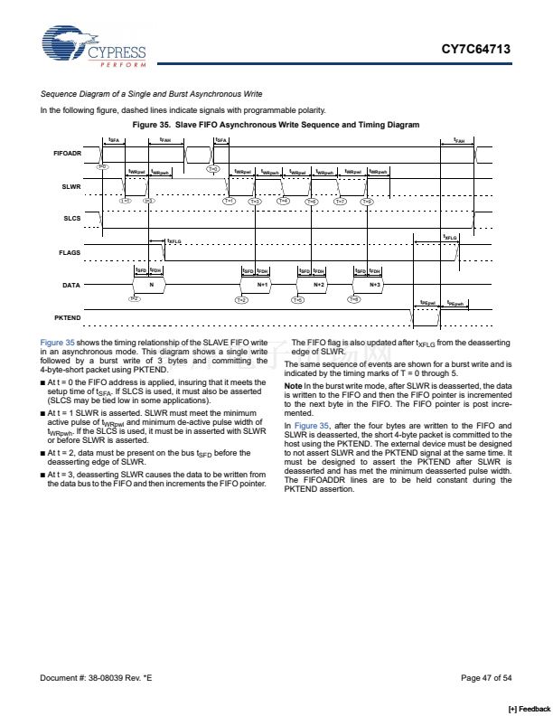
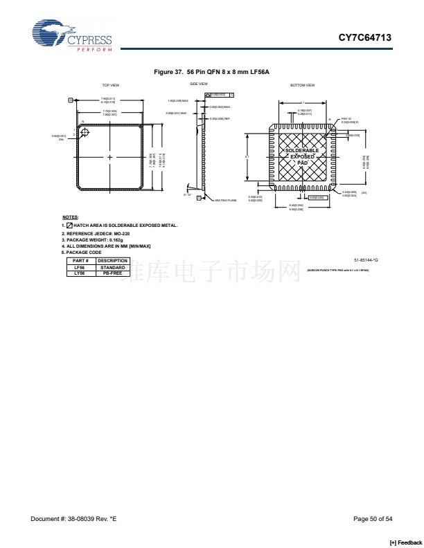
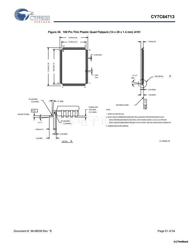
CY7C64713
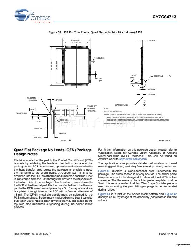
Figure 39. 128 Pin Thin Plastic Quad Flatpack (14 x 20 x 1.4 mm) A128
16.00卤0.20
14.00卤0.10
128
1
1.40卤0.05
0.22卤0.05
22.00卤0.20
20.00卤0.10
0.50
TYP.
12掳卤1掳
(8X)
SEE DETAIL
A
0.20 MAX.
1.60 MAX.
0.08
R 0.08 MIN.
0.20 MAX.
0掳 MIN.
STAND-OFF
0.05 MIN.
0.15 MAX.
SEATING PLANE
NOTE:
1. JEDEC STD REF MS-026
0.25
GAUGE PLANE
0掳-7掳
R 0.08 MIN.
0.20 MAX.
2. BODY LENGTH DIMENSION DOES NOT INCLUDE MOLD PROTRUSION/END FLASH
MOLD PROTRUSION/END FLASH SHALL NOT EXCEED 0.0098 in (0.25 mm) PER SIDE
BODY LENGTH DIMENSIONS ARE MAX PLASTIC BODY SIZE INCLUDING MOLD MISMATCH
3. DIMENSIONS IN MILLIMETERS
0.60卤0.15
0.20 MIN.
1.00 REF.
DETAIL
A
51-85101 *C
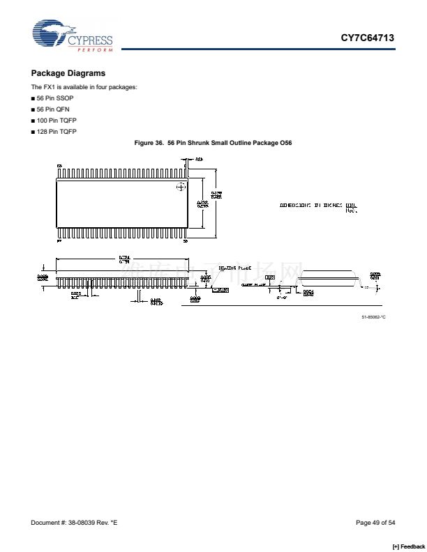
Quad Flat Package No Leads (QFN) Package
Design Notes
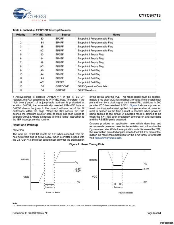
Electrical contact of the part to the Printed Circuit Board (PCB)
is made by soldering the leads on the bottom surface of the
package to the PCB. Aas a result, special attention is required to
the heat transfer area below the package to provide a good
thermal bond to the circuit board. A Copper (Cu) fill is to be
designed into the PCB as a thermal pad under the package. Heat
is transferred from the FX1 through the device鈥檚 metal paddle on
the bottom side of the package. Heat from here, is conducted to
the PCB at the thermal pad. It is then conducted from the thermal
pad to the PCB inner ground plane by a 5 x 5 array of via. A via
is a plated through hole in the PCB with a finished diameter of
13 mil. The QFN鈥檚 metal die paddle must be soldered to the
PCB鈥檚 thermal pad. Solder mask is placed on the board top side
over each via to resist solder flow into the via. The mask on the
top side also minimizes outgassing during the solder reflow
process.
For further information on this package design please refer to
鈥楢pplication Notes for Surface Mount Assembly of Amkor's
MicroLeadFrame (MLF) Packages鈥? This can be found on
Amkor's website
http://www.amkor.com.
The application note provides detailed information on board
mounting guidelines, soldering flow, rework process, and so on.
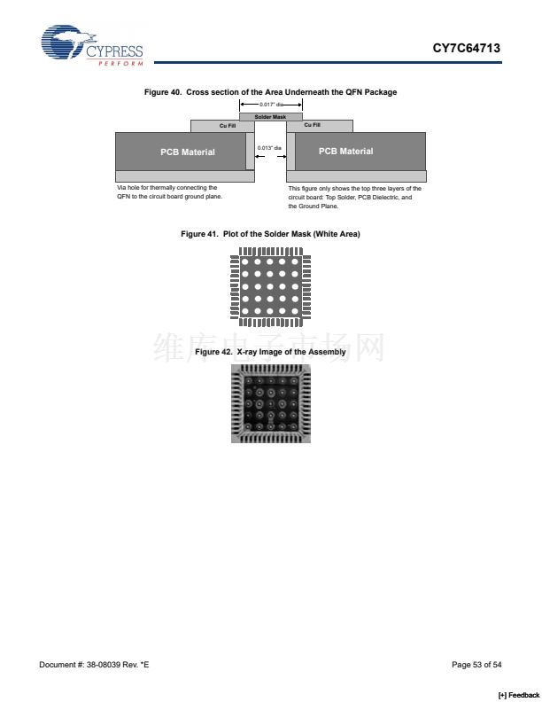
Figure 40
displays a cross-sectional area underneath the
package. The cross section is of only one via. The solder paste
template needs to be designed to allow at least 50% solder
coverage. The thickness of the solder paste template must be
5 mil. It is recommended that 鈥楴o Clean鈥?type 3 solder paste is
used for mounting the part. Nitrogen purge is recommended
during reflow.
Figure 41
is a plot of the solder mask pattern and
Figure 42
displays an X-Ray image of the assembly (darker areas indicate
solder).
Document #: 38-08039 Rev. *E
Page 52 of 54
[+] Feedback


 1
1
 2
2
 3
3
 4
4
 5
5
 6
6
 7
7
 8
8
 9
9
 10
10
 11
11
 12
12
 13
13
 14
14
 15
15
 16
16
 17
17
 18
18
 19
19
 20
20
 21
21
 22
22
 23
23
 24
24
 25
25
 26
26
 27
27
 28
28
 29
29
 30
30
 31
31
 32
32
 33
33
 34
34
 35
35
 36
36
 37
37
 38
38
 39
39
 40
40
 41
41
 42
42
 43
43
 44
44
 45
45
 46
46
 47
47
 48
48
 49
49
 50
50
 51
51
 52
52
 53
53
 54
54
