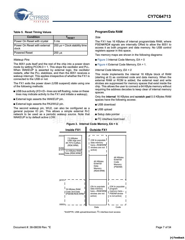
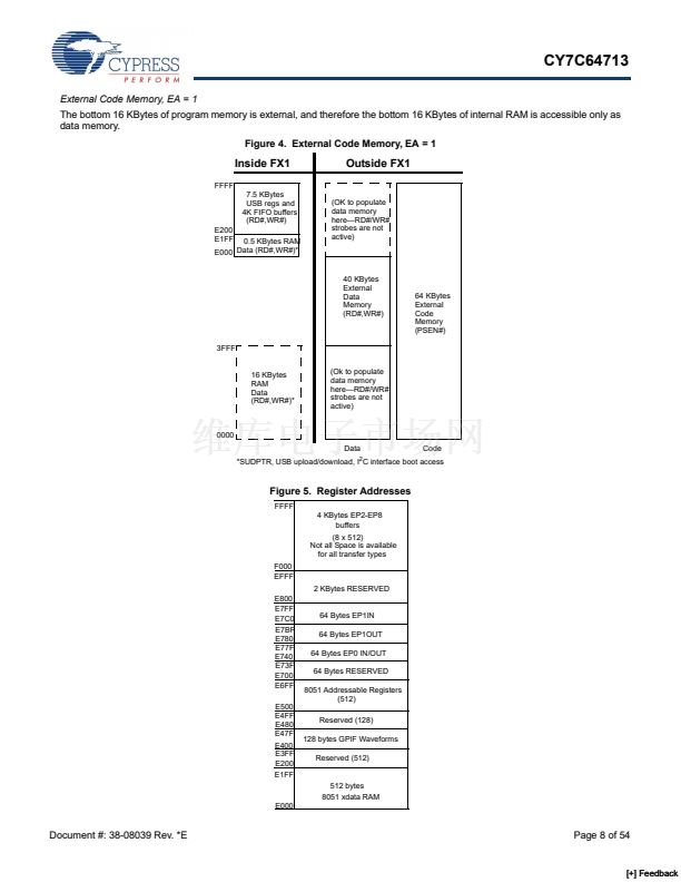
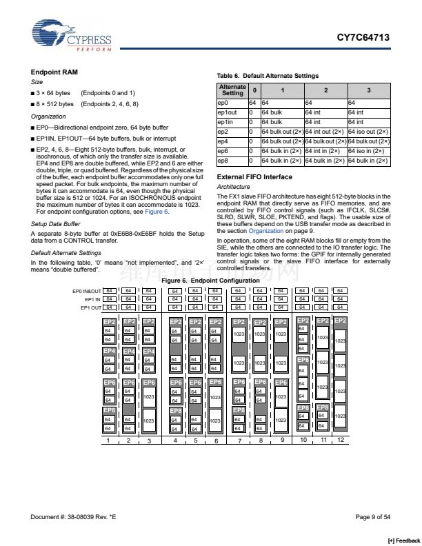
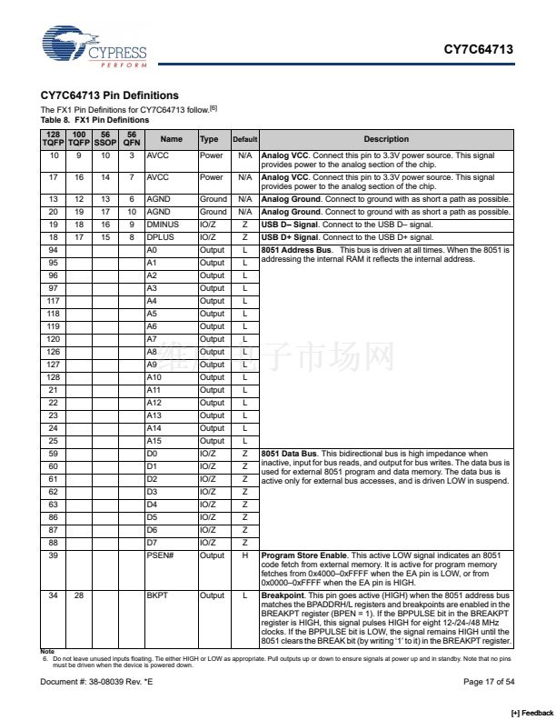
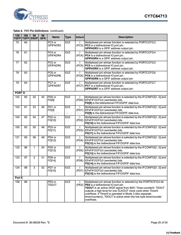
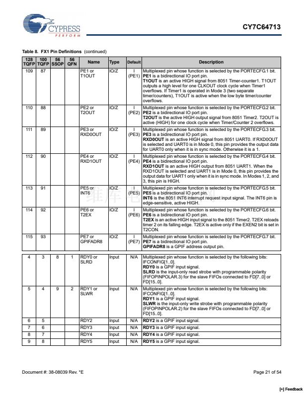
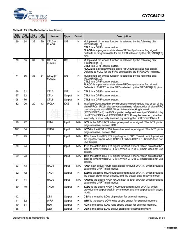
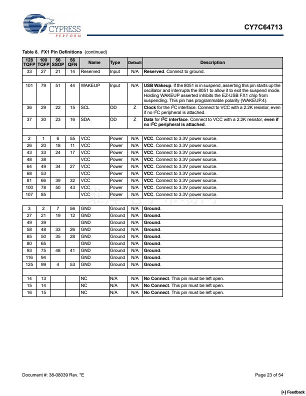
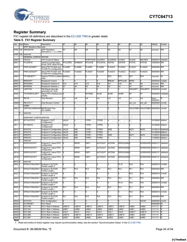
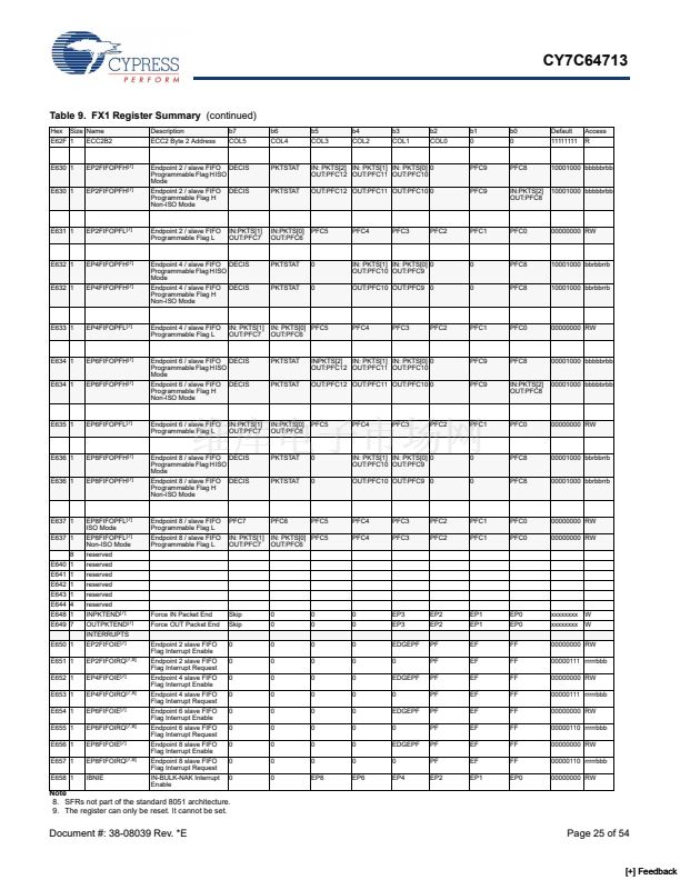
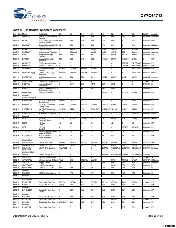
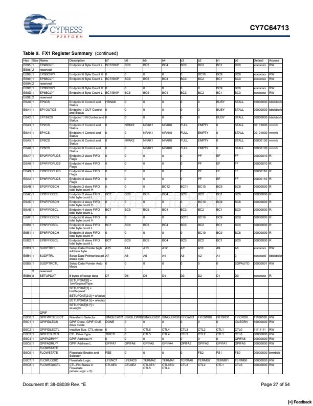
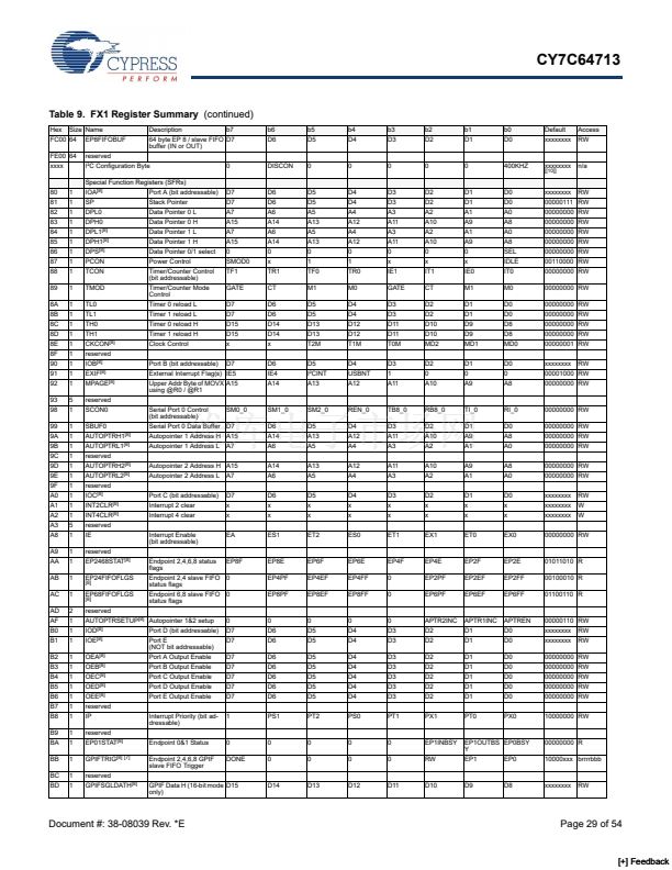
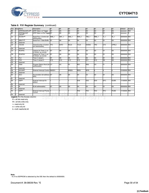
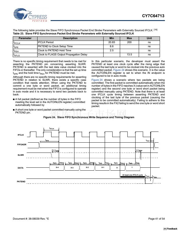
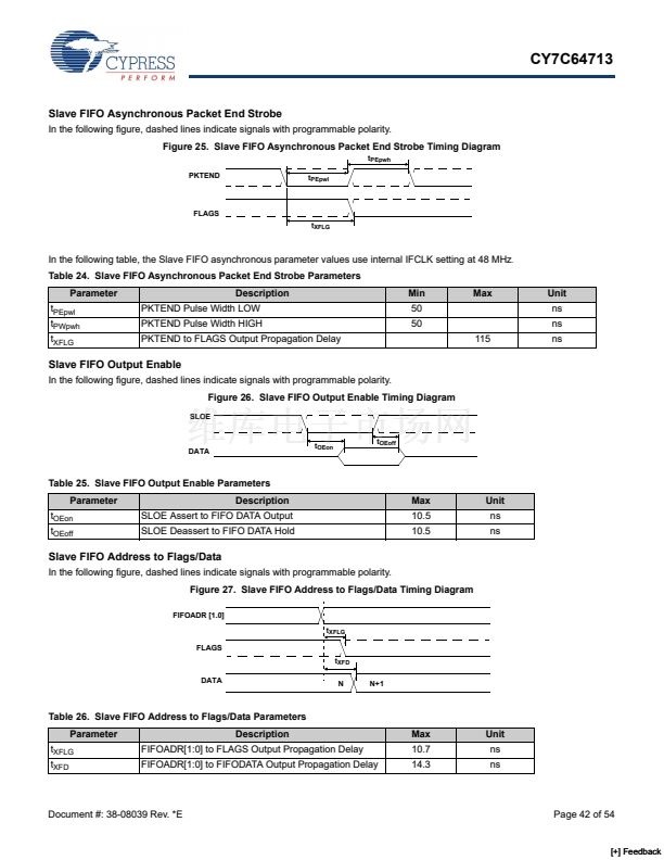
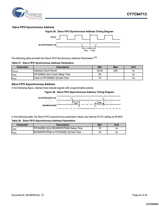
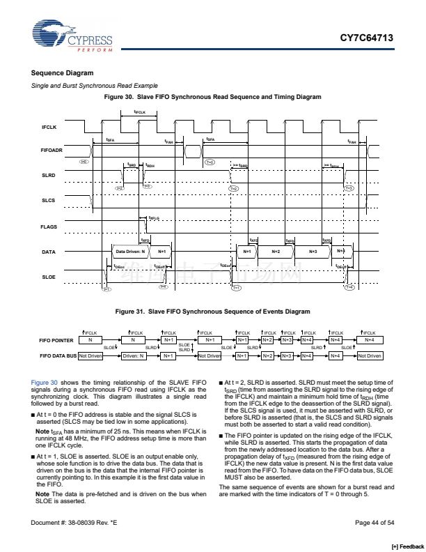
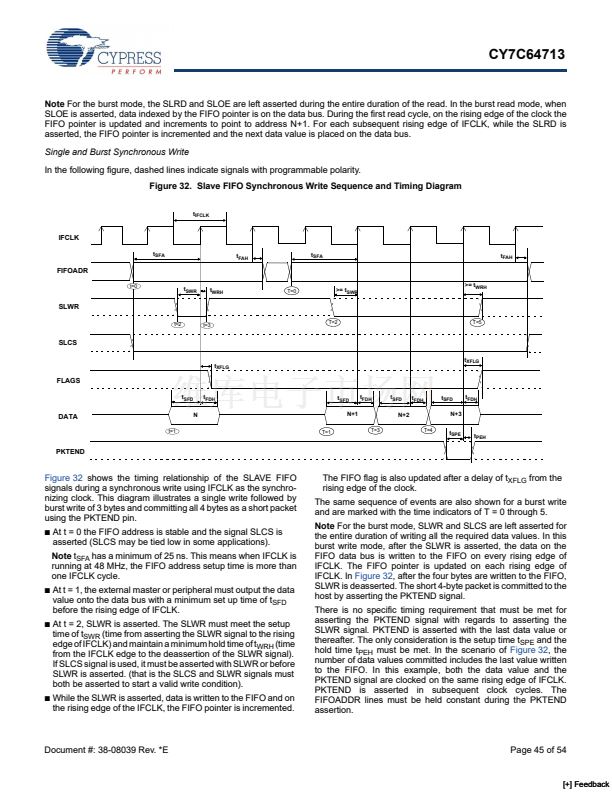
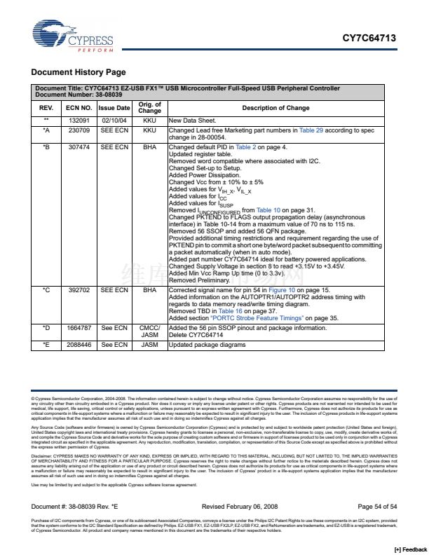
CY7C64713
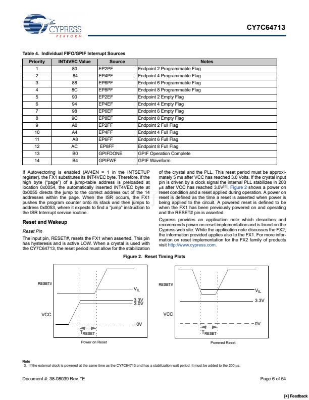
Table 4. Individual FIFO/GPIF Interrupt Sources
Priority
1
2
3
4
5
6
7
8
9
10
11
12
13
14
INT4VEC Value
80
84
88
8C
90
94
98
9C
A0
A4
A8
AC
B0
B4
Source
EP2PF
EP4PF
EP6PF
EP8PF
EP2EF
EP4EF
EP6EF
EP8EF
EP2FF
EP4FF
EP6FF
EP8FF
GPIFDONE
GPIFWF
Notes
Endpoint 2 Programmable Flag
Endpoint 4 Programmable Flag
Endpoint 6 Programmable Flag
Endpoint 8 Programmable Flag
Endpoint 2 Empty Flag
Endpoint 4 Empty Flag
Endpoint 6 Empty Flag
Endpoint 8 Empty Flag
Endpoint 2 Full Flag
Endpoint 4 Full Flag
Endpoint 6 Full Flag
Endpoint 8 Full Flag
GPIF Operation Complete
GPIF Waveform
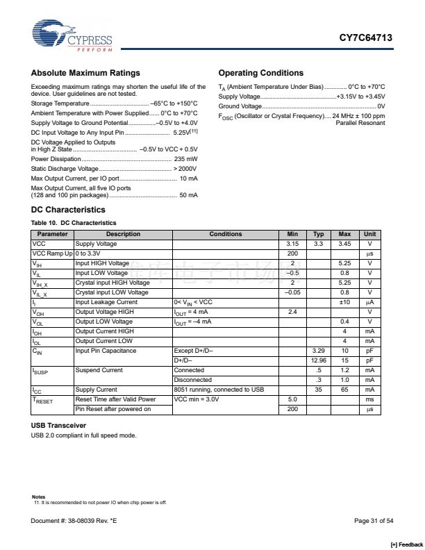
of the crystal and the PLL. This reset period must be approxi-
mately 5 ms after VCC has reached 3.0 Volts. If the crystal input
pin is driven by a clock signal the internal PLL stabilizes in 200
渭s
after VCC has reached 3.0V
[3]
.
Figure 2
shows a power on
reset condition and a reset applied during operation. A power on
reset is defined as the time a reset is asserted when power is
being applied to the circuit. A powered reset is defined to be
when the FX1 has been previously powered on and operating
and the RESET# pin is asserted.
Cypress provides an application note which describes and
recommends power on reset implementation and is found on the
Cypress web site. While the application note discusses the FX2,
the information provided applies also to the FX1. For more infor-
mation on reset implementation for the FX2 family of products
visit
http://www.cypress.com.
If Autovectoring is enabled (AV4EN = 1 in the INTSETUP
register), the FX1 substitutes its INT4VEC byte. Therefore, if the
high byte (鈥減age鈥? of a jump-table address is preloaded at
location 0x0054, the automatically inserted INT4VEC byte at
0x0055 directs the jump to the correct address out of the 14
addresses within the page. When the ISR occurs, the FX1
pushes the program counter onto its stack and then jumps to
address 0x0053, where it expects to find a 鈥渏ump鈥?instruction to
the ISR Interrupt service routine.
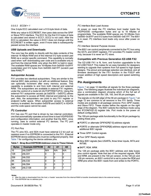
Reset and Wakeup
Reset Pin
The input pin, RESET#, resets the FX1 when asserted. This pin
has hysteresis and is active LOW. When a crystal is used with
the CY7C64713, the reset period must allow for the stabilization
Figure 2. Reset Timing Plots
RESET#
RESET#
V
IL
3.3V
3.0V
VCC
0V
T
RESET
Power on Reset
V
IL
3.3V
VCC
0V
T
RESET
Powered Reset
Note
3. If the external clock is powered at the same time as the CY7C64713 and has a stabilization wait period. It must be added to the 200
渭s.
Document #: 38-08039 Rev. *E
Page 6 of 54
[+] Feedback


 1
1
 2
2
 3
3
 4
4
 5
5
 6
6
 7
7
 8
8
 9
9
 10
10
 11
11
 12
12
 13
13
 14
14
 15
15
 16
16
 17
17
 18
18
 19
19
 20
20
 21
21
 22
22
 23
23
 24
24
 25
25
 26
26
 27
27
 28
28
 29
29
 30
30
 31
31
 32
32
 33
33
 34
34
 35
35
 36
36
 37
37
 38
38
 39
39
 40
40
 41
41
 42
42
 43
43
 44
44
 45
45
 46
46
 47
47
 48
48
 49
49
 50
50
 51
51
 52
52
 53
53
 54
54
