鈮?/div>
V
IH
).
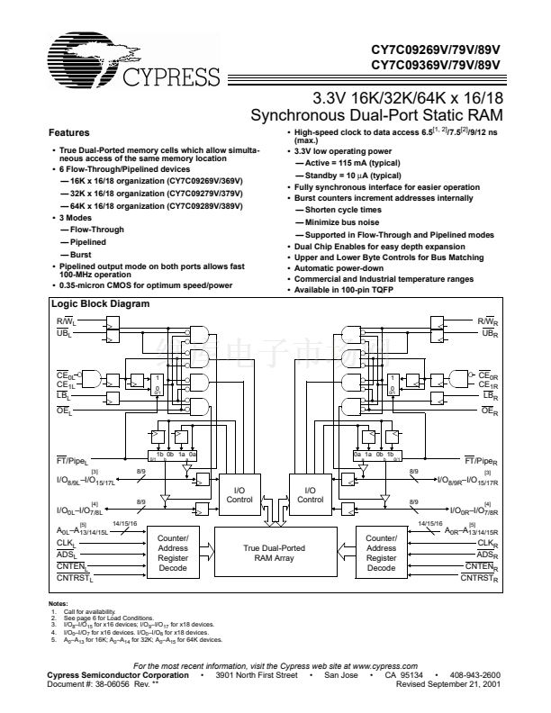
Clock Signal. This input can be free running or strobed. Maximum clock input rate is f
MAX
.
Counter Enable Input. Asserting this signal LOW increments the burst address counter of its
respective port on each rising edge of CLK. CNTEN is disabled if ADS or CNTRST are asserted
LOW.
Counter Reset Input. Asserting this signal LOW resets the burst address counter of its respec-
tive port to zero. CNTRST is not disabled by asserting ADS or CNTEN.
Data Bus Input/Output (I/O
0
鈥揑/O
15
for x16 devices).
Lower Byte Select Input. Asserting this signal LOW enables read and write operations to the
lower byte. (I/O
0
鈥揑/O
8
for x18, I/O
0
鈥揑/O
7
for x16) of the memory array. For read operations both
the LB and OE signals must be asserted to drive output data on the lower byte of the data pins.
Upper Byte Select Input. Same function as LB, but to the upper byte (I/O
8/9L
鈥揑/O
15/17L
).
Output Enable Input. This signal must be asserted LOW to enable the I/O data pins during read
operations.
Read/Write Enable Input. This signal is asserted LOW to write to the dual port memory array.
For read operations, assert this pin HIGH.
Flow-Through/Pipelined Select Input. For flow-through mode operation, assert this pin LOW.
For pipelined mode operation, assert this pin HIGH.
Ground Input.
No Connect.
Power Input.
Output Current into Outputs (LOW)............................. 20 mA
Static Discharge Voltage ........................................... >1100V
Latch-Up Current...................................................... >200mA
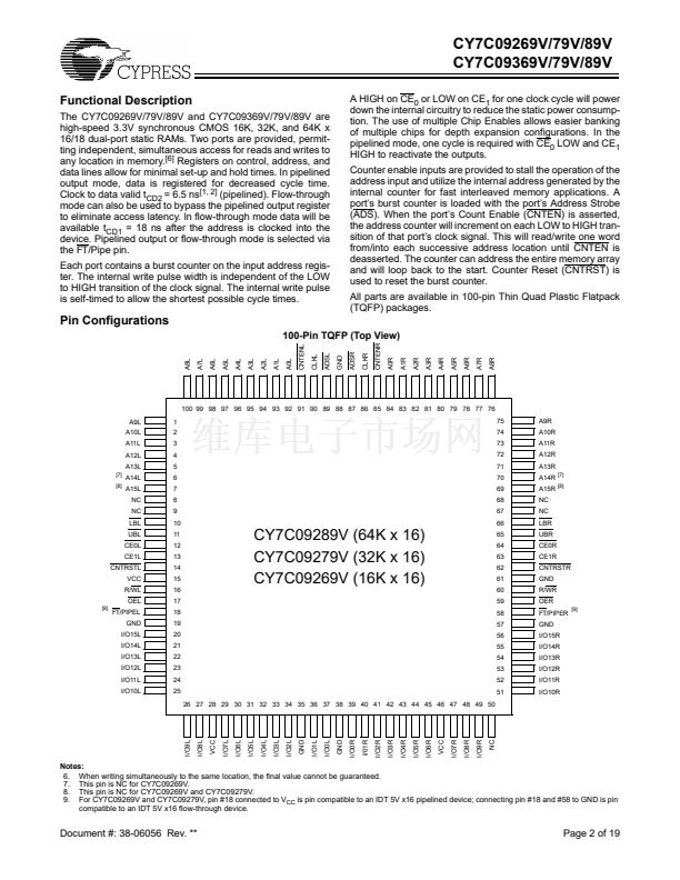
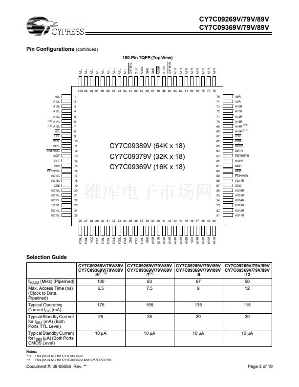
CE
0L
,CE
1L
CLK
L
CNTEN
L
CE
0R
,CE
1R
CLK
R
CNTEN
R
CNTRST
L
I/O
0L
鈥揑/O
17L
LB
L
CNTRST
R
I/O
0R
鈥揑/O
17R
LB
R
UB
L
OE
L
R/W
L
FT/PIPE
L
GND
NC
V
CC
UB
R
OE
R
R/W
R
FT/PIPE
R
Maximum Ratings
(Above which the useful life may be impaired. For user guide-
lines, not tested.)
Storage Temperature ................................. 鈥?5
掳
C to +150
掳
C
Ambient Temperature with
Power Applied.............................................鈥?5
掳
C to +125
掳
C
Supply Voltage to Ground Potential ............... 鈥?.5V to +4.6V
DC Voltage Applied to
Outputs in High Z State ...........................鈥?.5V to V
CC
+0.5V
DC Input Voltage......................................鈥?.5V to V
CC
+0.5V
Operating Range
Range
Commercial
Industrial
Ambient
Temperature
0
掳
C to +70
掳
C
鈥?0
掳
C to +85
掳
C
V
CC
3.3V
卤
300 mV
3.3V
卤
300 mV
Document #: 38-06056 Rev. **
Page 4 of 19


 1
1
 2
2
 3
3
 4
4
 5
5
 6
6
 7
7
 8
8
 9
9
 10
10
 11
11
 12
12
 13
13
 14
14
 15
15
 16
16
 17
17
 18
18
 19
19
