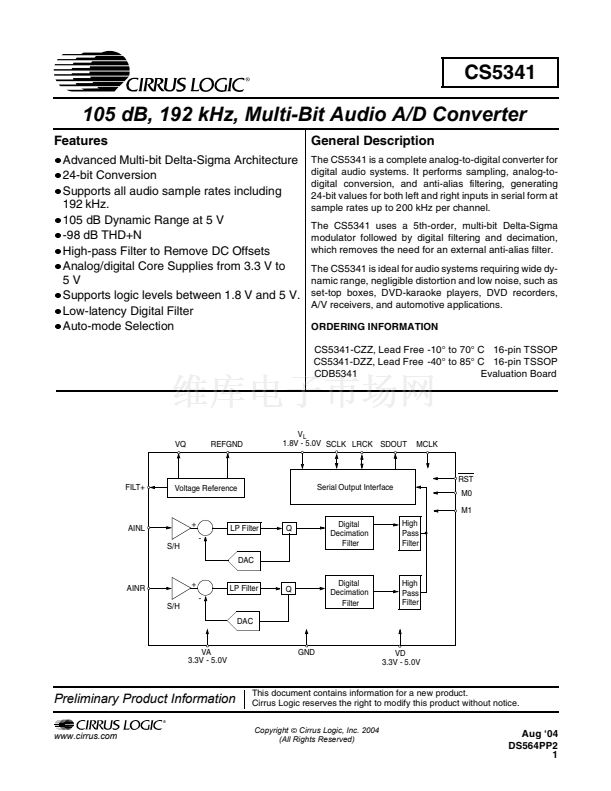
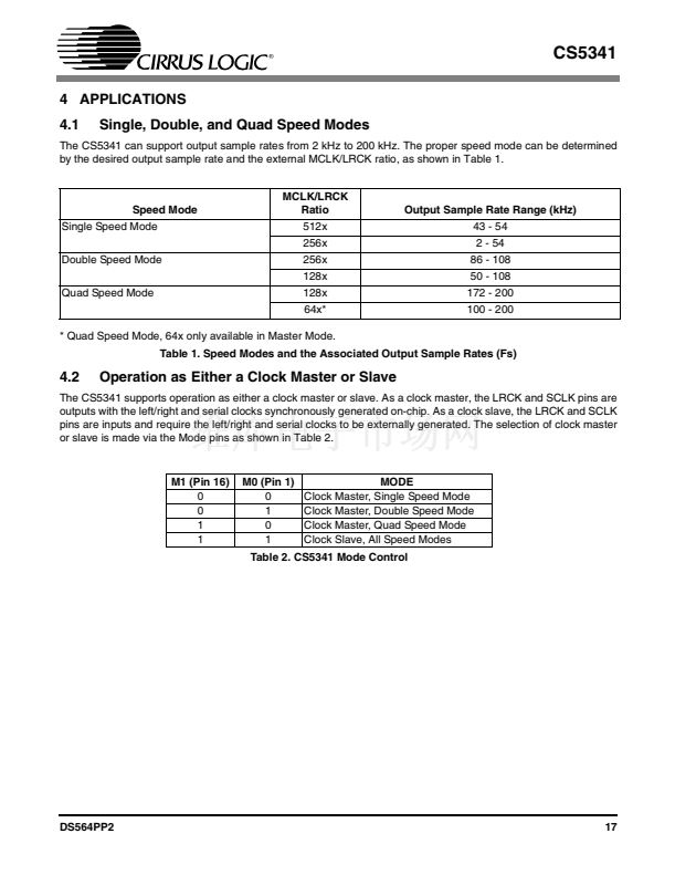
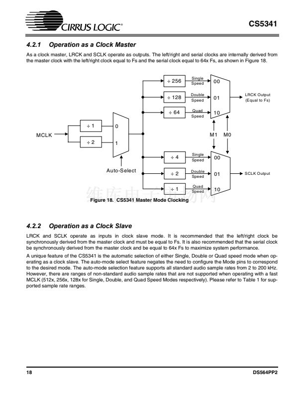
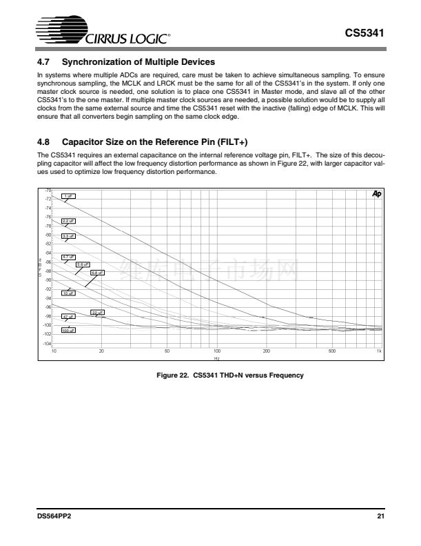
鈩?/div>
C S 5341 A IN R
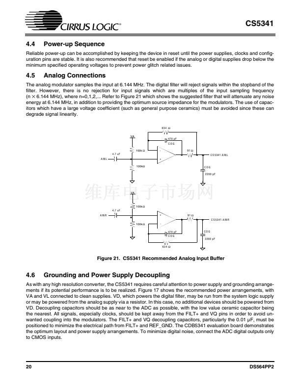
Figure 21. CS5341 Recommended Analog Input Buffer
4.6
Grounding and Power Supply Decoupling
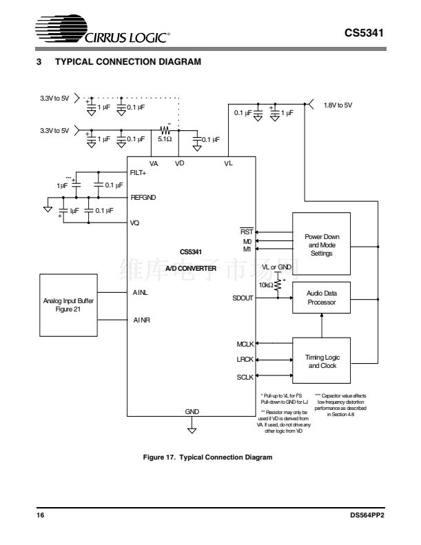
As with any high resolution converter, the CS5341 requires careful attention to power supply and grounding arrange-
ments if its potential performance is to be realized. Figure 17 shows the recommended power arrangements, with
VA and VL connected to clean supplies. VD, which powers the digital filter, may be run from the system logic supply
or may be powered from the analog supply via a resistor. In this case, no additional devices should be powered from
VD. Decoupling capacitors should be as near to the ADC as possible, with the low value ceramic capacitor being
the nearest. All signals, especially clocks, should be kept away from the FILT+ and VQ pins in order to avoid un-
wanted coupling into the modulators. The FILT+ and VQ decoupling capacitors, particularly the 0.01 碌F, must be
positioned to minimize the electrical path from FILT+ and REF_GND. The CDB5341 evaluation board demonstrates
the optimum layout and power supply arrangements. To minimize digital noise, connect the ADC digital outputs only
to CMOS inputs.
20
DS564PP2


 1
1
 2
2
 3
3
 4
4
 5
5
 6
6
 7
7
 8
8
 9
9
 10
10
 11
11
 12
12
 13
13
 14
14
 15
15
 16
16
 17
17
 18
18
 19
19
 20
20
 21
21
 22
22
 23
23
 24
24
