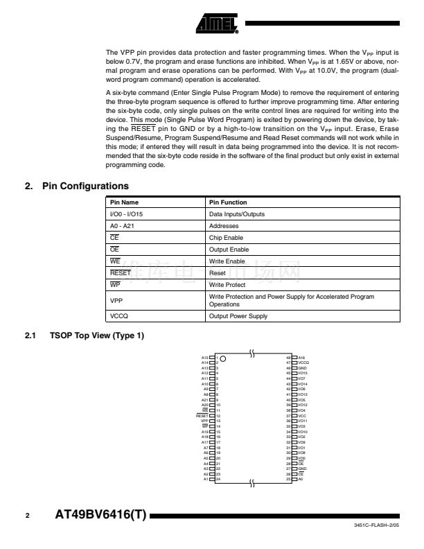
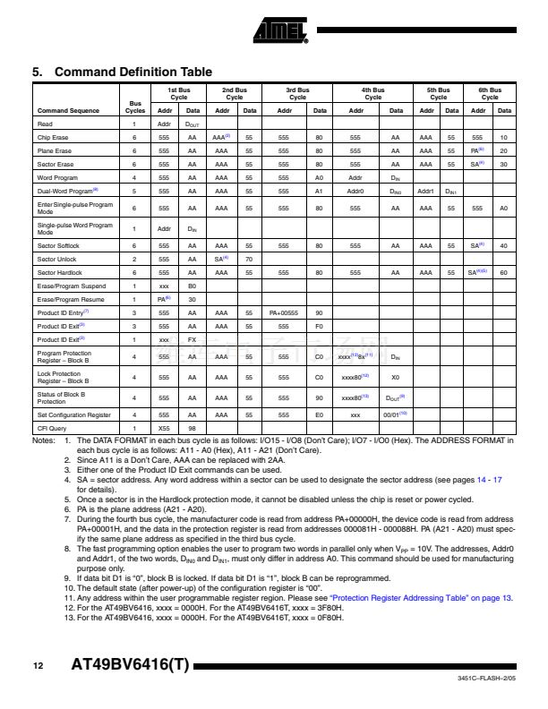
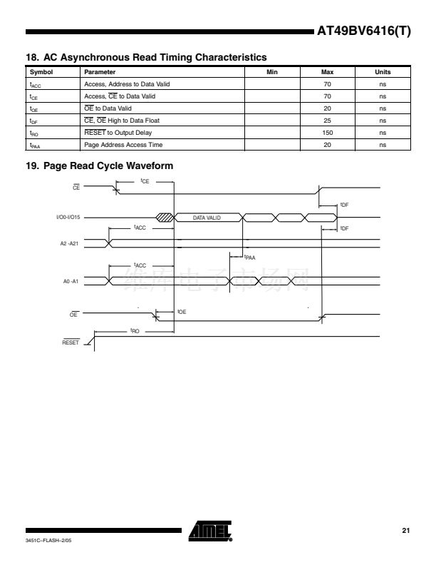
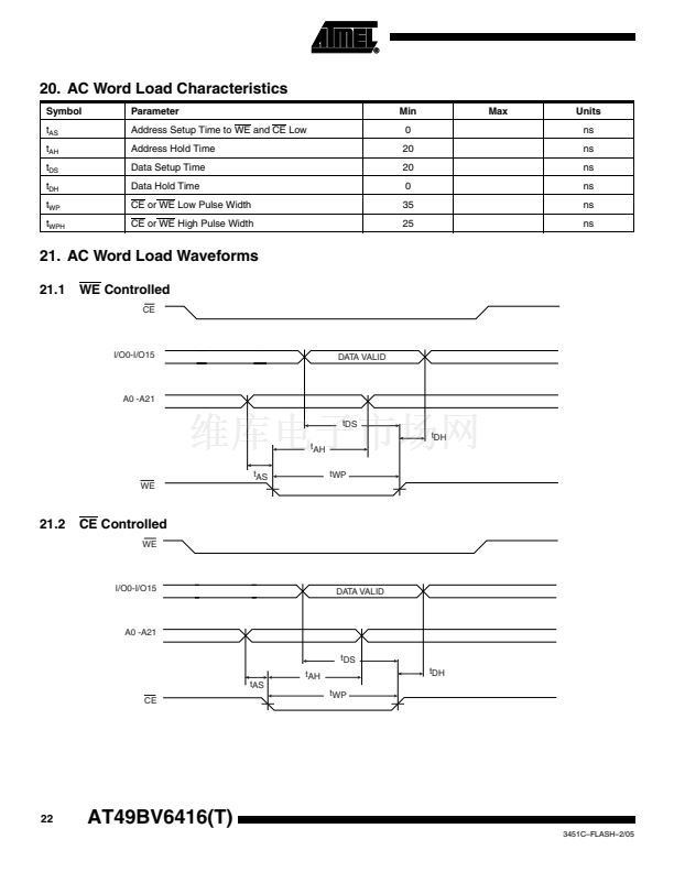
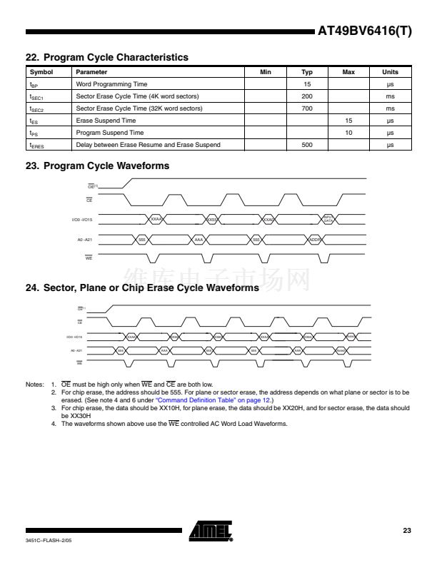
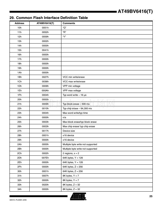
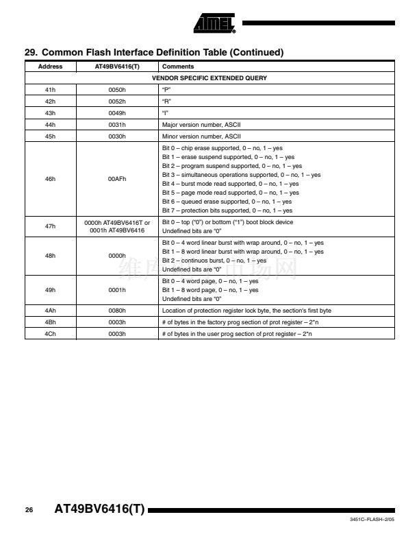
5. Command Definition Table
1st Bus
Cycle
Command Sequence
Read
Chip Erase
Plane Erase
Sector Erase
Word Program
Dual-Word Program
(8)
Enter Single-pulse Program
Mode
Single-pulse Word Program
Mode
Sector Softlock
Sector Unlock
Sector Hardlock
Erase/Program Suspend
Erase/Program Resume
Product ID Entry
(7)
Product ID Exit
(3)
Product ID Exit
(3)
Program Protection
Register 鈥?Block B
Lock Protection
Register 鈥?Block B
Status of Block B
Protection
Set Configuration Register
CFI Query
Bus
Cycles
1
6
6
6
4
5
6
1
6
2
6
1
1
3
3
1
4
4
4
4
1
Addr
Addr
555
555
555
555
555
555
Addr
555
555
555
xxx
PA
(6)
555
555
xxx
555
555
555
555
X55
Data
D
OUT
AA
AA
AA
AA
AA
AA
D
IN
AA
AA
AA
B0
30
AA
AA
FX
AA
AA
AA
AA
98
AAA
AAA
AAA
AAA
55
55
55
55
555
555
555
555
C0
C0
90
E0
xxxx
(12)
8x
(11)
xxxx80
(12)
xxxx80
(13)
xxx
D
IN
X0
D
OUT(9)
00/01
(10)
AAA
AAA
55
55
PA+00555
555
90
F0
AAA
SA
(4)
AAA
55
70
55
555
80
555
AA
AAA
55
SA
(4)(5)
60
555
80
555
AA
AAA
55
SA
(4)
40
AAA
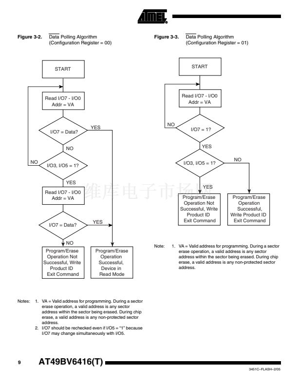
(2)
AAA
AAA
AAA
AAA
AAA
55
55
55
55
55
55
555
555
555
555
555
555
80
80
80
A0
A1
80
555
555
555
Addr
Addr0
555
AA
AA
AA
D
IN
D
IN0
AA
Addr1
AAA
D
IN1
55
555
A0
AAA
AAA
AAA
55
55
55
555
PA
(6)
SA
(4)
10
20
30
2nd Bus
Cycle
Addr
Data
3rd Bus
Cycle
Addr
Data
4th Bus
Cycle
Addr
Data
5th Bus
Cycle
Addr
Data
6th Bus
Cycle
Addr
Data
Notes:
1. The DATA FORMAT in each bus cycle is as follows: I/O15 - I/O8 (Don鈥檛 Care); I/O7 - I/O0 (Hex). The ADDRESS FORMAT in
each bus cycle is as follows: A11 - A0 (Hex), A11 - A21 (Don鈥檛 Care).
2. Since A11 is a Don鈥檛 Care, AAA can be replaced with 2AA.
3. Either one of the Product ID Exit commands can be used.
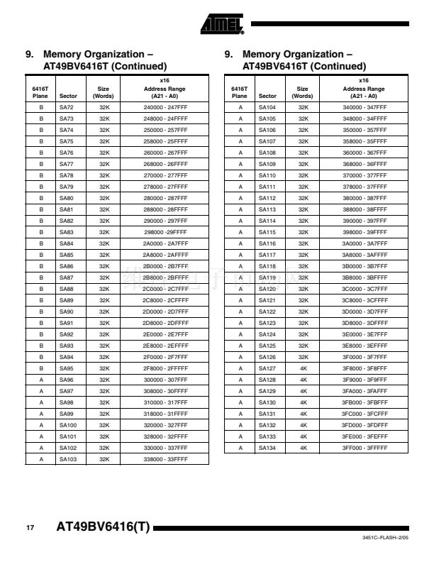
4. SA = sector address. Any word address within a sector can be used to designate the sector address (see pages
14
-
17
for details).
5. Once a sector is in the Hardlock protection mode, it cannot be disabled unless the chip is reset or power cycled.
6. PA is the plane address (A21 - A20).
7. During the fourth bus cycle, the manufacturer code is read from address PA+00000H, the device code is read from address
PA+00001H, and the data in the protection register is read from addresses 000081H - 000088H. PA (A21 - A20) must spec-
ify the same plane address as specified in the third bus cycle.
8. The fast programming option enables the user to program two words in parallel only when V
PP
= 10V. The addresses, Addr0
and Addr1, of the two words, D
IN0
and D
IN1
, must only differ in address A0. This command should be used for manufacturing
purpose only.
9. If data bit D1 is 鈥?鈥? block B is locked. If data bit D1 is 鈥?鈥? block B can be reprogrammed.
10. The default state (after power-up) of the configuration register is 鈥?0鈥?
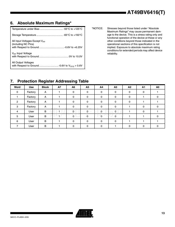
11. Any address within the user programmable register region. Please see
鈥淧rotection Register Addressing Table鈥?on page 13.
12. For the AT49BV6416, xxxx = 0000H. For the AT49BV6416T, xxxx = 3F80H.
13. For the AT49BV6416, xxxx = 0000H. For the AT49BV6416T, xxxx = 0F80H.
12
AT49BV6416(T)
3451C鈥揊LASH鈥?/05


 1
1
 2
2
 3
3
 4
4
 5
5
 6
6
 7
7
 8
8
 9
9
 10
10
 11
11
 12
12
 13
13
 14
14
 15
15
 16
16
 17
17
 18
18
 19
19
 20
20
 21
21
 22
22
 23
23
 24
24
 25
25
 26
26
 27
27
 28
28
 29
29
 30
30
