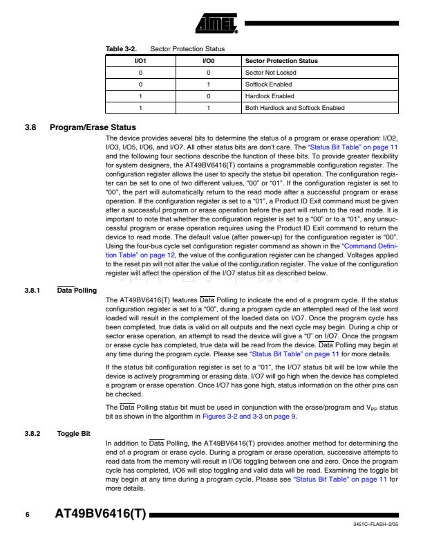
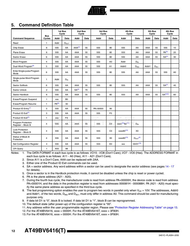
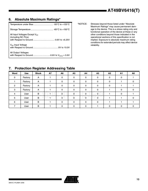
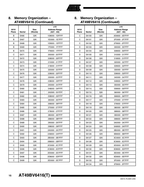
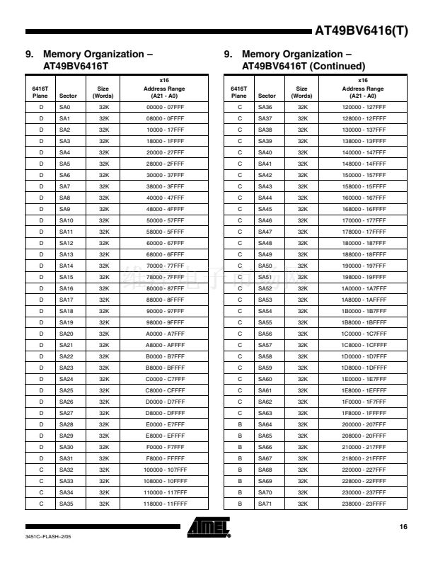
Table 3-2.
I/O1
0
0
1
1
Sector Protection Status
I/O0
0
1
0
1
Sector Protection Status
Sector Not Locked
Softlock Enabled
Hardlock Enabled
Both Hardlock and Softlock Enabled
3.8
Program/Erase Status
The device provides several bits to determine the status of a program or erase operation: I/O2,
I/O3, I/O5, I/O6, and I/O7. All other status bits are don鈥檛 care. The
鈥淪tatus Bit Table鈥?on page 11
and the following four sections describe the function of these bits. To provide greater flexibility
for system designers, the AT49BV6416(T) contains a programmable configuration register. The
configuration register allows the user to specify the status bit operation. The configuration regis-
ter can be set to one of two different values, 鈥?0鈥?or 鈥?1鈥? If the configuration register is set to
鈥?0鈥? the part will automatically return to the read mode after a successful program or erase
operation. If the configuration register is set to a 鈥?1鈥? a Product ID Exit command must be given
after a successful program or erase operation before the part will return to the read mode. It is
important to note that whether the configuration register is set to a 鈥?0鈥?or to a 鈥?1鈥? any unsuc-
cessful program or erase operation requires using the Product ID Exit command to return the
device to read mode. The default value (after power-up) for the configuration register is 鈥?0鈥?
Using the four-bus cycle set configuration register command as shown in the
鈥淐ommand Defini-
tion Table鈥?on page 12,
the value of the configuration register can be changed. Voltages applied
to the reset pin will not alter the value of the configuration register. The value of the configuration
register will affect the operation of the I/O7 status bit as described below.
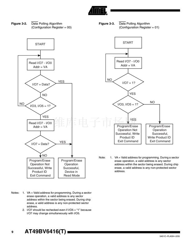
3.8.1
Data Polling
The AT49BV6416(T) features Data Polling to indicate the end of a program cycle. If the status
configuration register is set to a 鈥?0鈥? during a program cycle an attempted read of the last word
loaded will result in the complement of the loaded data on I/O7. Once the program cycle has
been completed, true data is valid on all outputs and the next cycle may begin. During a chip or
sector erase operation, an attempt to read the device will give a 鈥?鈥?on I/O7. Once the program
or erase cycle has completed, true data will be read from the device. Data Polling may begin at
any time during the program cycle. Please see
鈥淪tatus Bit Table鈥?on page 11
for more details.
If the status bit configuration register is set to a 鈥?1鈥? the I/O7 status bit will be low while the
device is actively programming or erasing data. I/O7 will go high when the device has completed
a program or erase operation. Once I/O7 has gone high, status information on the other pins can
be checked.
The Data Polling status bit must be used in conjunction with the erase/program and V
PP
status
bit as shown in the algorithm in
Figures 3-2 and 3-3
on
page 9.
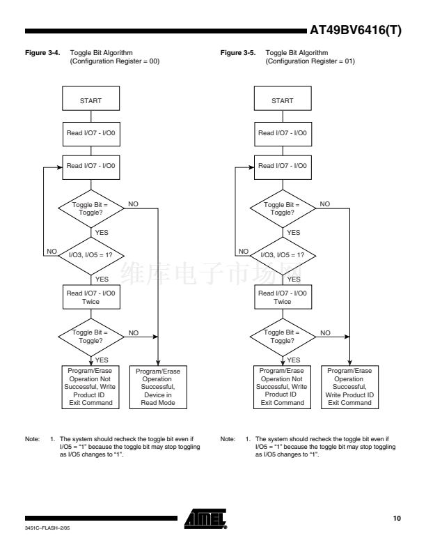
3.8.2
Toggle Bit
In addition to Data Polling, the AT49BV6416(T) provides another method for determining the
end of a program or erase cycle. During a program or erase operation, successive attempts to
read data from the memory will result in I/O6 toggling between one and zero. Once the program
cycle has completed, I/O6 will stop toggling and valid data will be read. Examining the toggle bit
may begin at any time during a program cycle. Please see
鈥淪tatus Bit Table鈥?on page 11
for
more details.
6
AT49BV6416(T)
3451C鈥揊LASH鈥?/05


 1
1
 2
2
 3
3
 4
4
 5
5
 6
6
 7
7
 8
8
 9
9
 10
10
 11
11
 12
12
 13
13
 14
14
 15
15
 16
16
 17
17
 18
18
 19
19
 20
20
 21
21
 22
22
 23
23
 24
24
 25
25
 26
26
 27
27
 28
28
 29
29
 30
30
