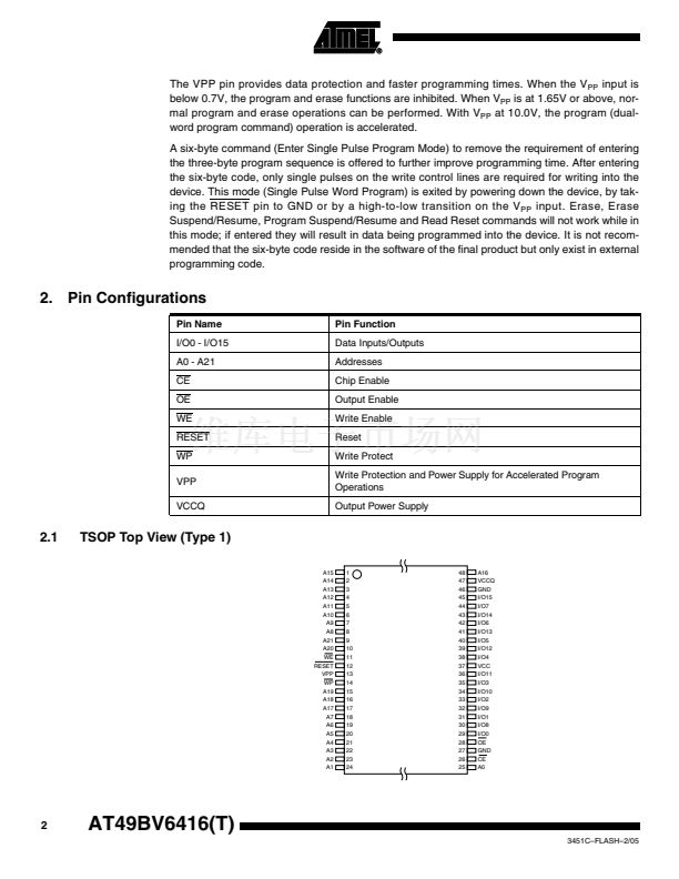
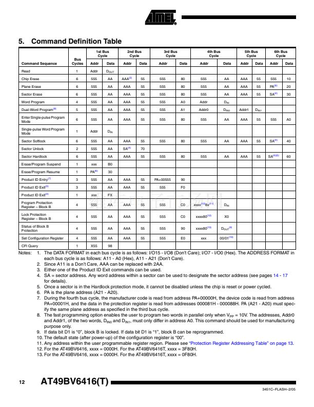
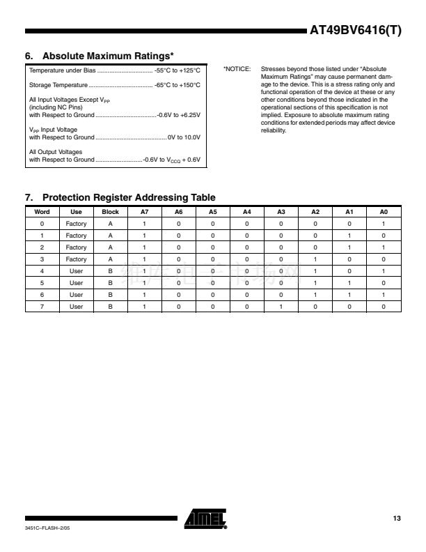
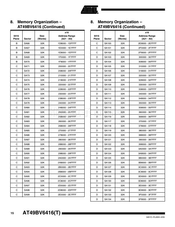
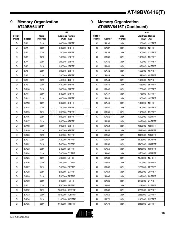
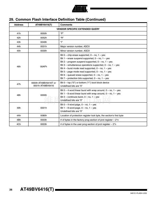
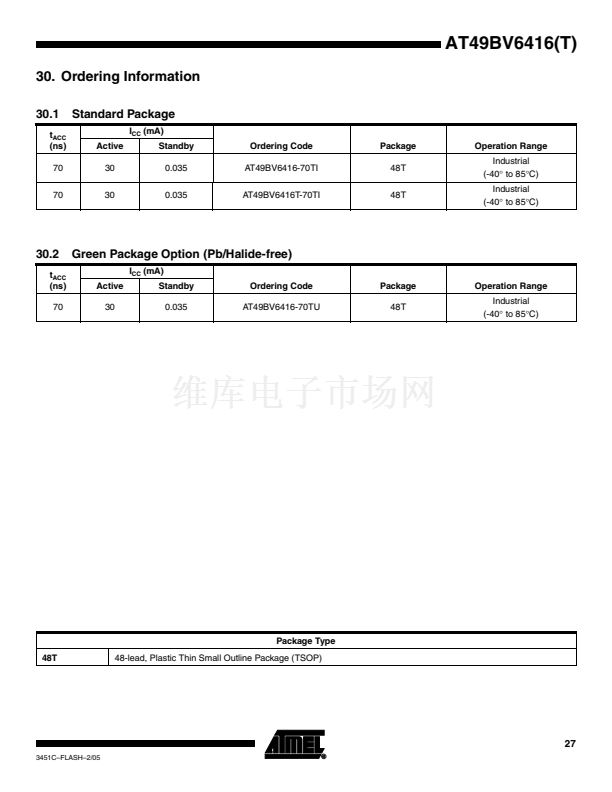
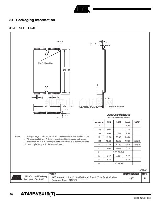
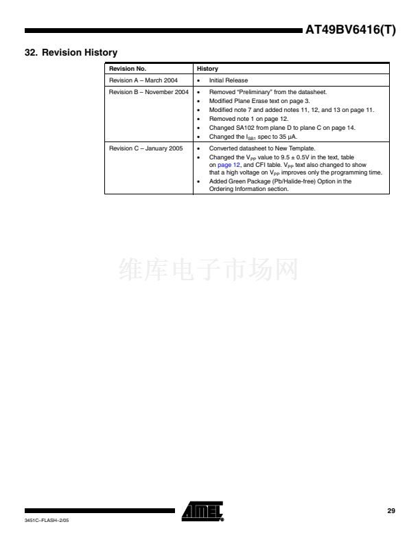
AT49BV6416(T)
3. Device Operation
3.1
Command Sequences
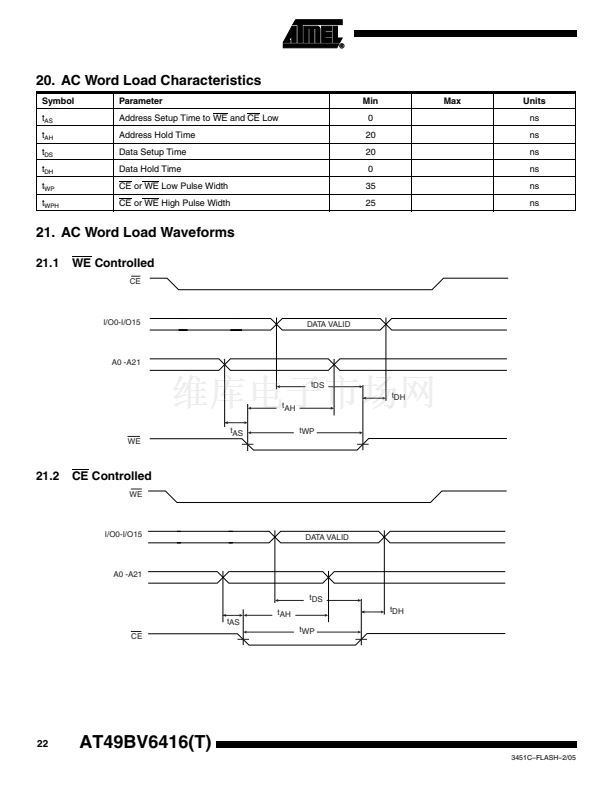
The device powers on in the read mode. Command sequences are used to place the device in
other operating modes such as program and erase. After the completion of a program or an
erase cycle, the device enters the read mode. The command sequences are written by applying
a low pulse on the WE input with CE low and OE high or by applying a low-going pulse on the
CE input with WE low and OE high. The address is latched on the falling edge of the WE or CE
pulse whichever occurs first. Valid data is latched on the rising edge of the WE or the CE pulse,
whichever occurs first. The addresses used in the command sequences are not affected by
entering the command sequences.
3.2
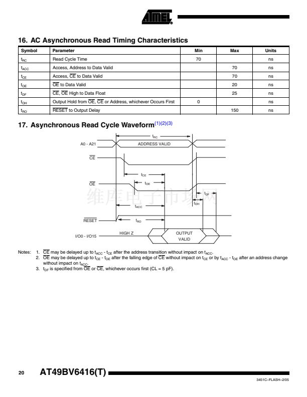
Asynchronous Read
The AT49BV6416(T) is accessed like an EPROM. When CE and OE are low and WE is high, the
data stored at the memory location determined by the address pins are asserted on the outputs.
The outputs are put in the high impedance state whenever CE or OE is high. This dual-line con-
trol gives designers flexibility in preventing bus contention.
3.3
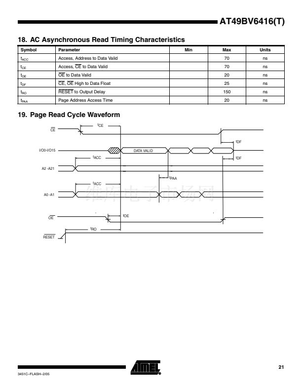
Page Read
The page read operation of the device is controlled by CE and OE inputs. The page size is four
words. The first word access of the page read is the same as the asynchronous read. The first
word is read at an asynchronous speed of 70 ns. Once the first word is read, toggling A0 and A1
will result in subsequent reads within the page being output at a speed of 20 ns. The
鈥淧age
Read Cycle Waveform鈥?/span>
is shown on
page 21.
3.4
Reset
A RESET input pin is provided to ease some system applications. When RESET is at a logic
high level, the device is in its standard operating mode. A low level on the RESET pin halts the
present device operation and puts the outputs of the device in a high-impedance state. When a
high level is reasserted on the RESET pin, the device returns to read or standby mode, depend-
ing upon the state of the control pins.
3.5
Erase
Before a word can be reprogrammed it must be erased. The erased state of the memory bits is a
logical 鈥?鈥? The entire memory can be erased by using the Chip Erase command or individual
planes or sectors can be erased by using the Plane Erase or Sector Erase commands.
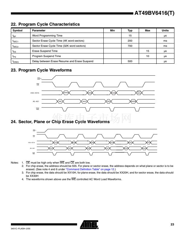
3.5.1
Chip Erase
Chip Erase is a six-bus cycle operation. The automatic erase begins on the rising edge of the
last WE pulse. Chip Erase does not alter the data of the protected sectors. After the full chip
erase the device will return back to the read mode. The hardware reset during Chip Erase will
stop the erase but the data will be of unknown state. Any command during Chip Erase except
Erase Suspend will be ignored.
3
3451C鈥揊LASH鈥?/05


 1
1
 2
2
 3
3
 4
4
 5
5
 6
6
 7
7
 8
8
 9
9
 10
10
 11
11
 12
12
 13
13
 14
14
 15
15
 16
16
 17
17
 18
18
 19
19
 20
20
 21
21
 22
22
 23
23
 24
24
 25
25
 26
26
 27
27
 28
28
 29
29
 30
30
