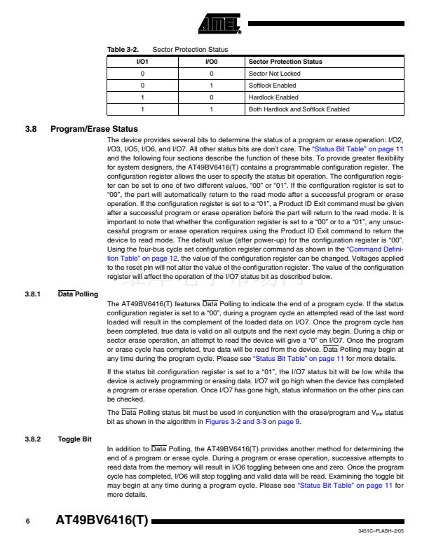
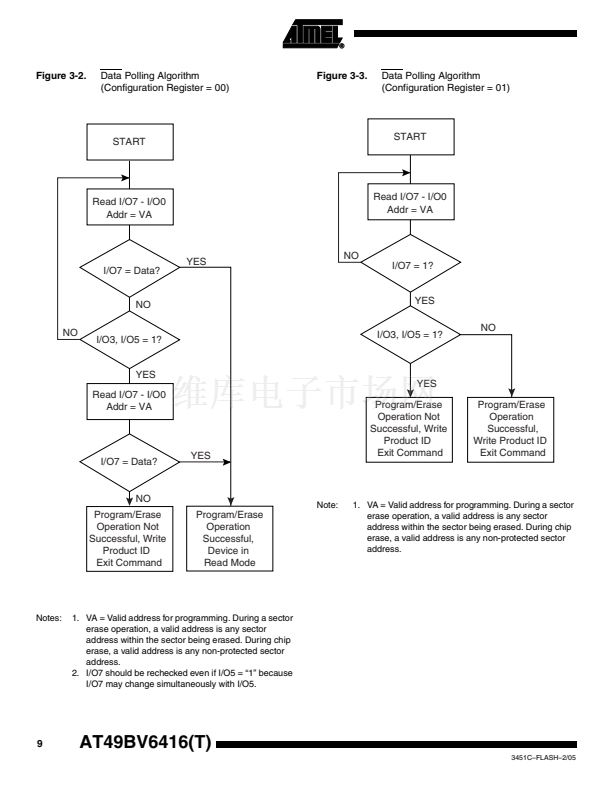
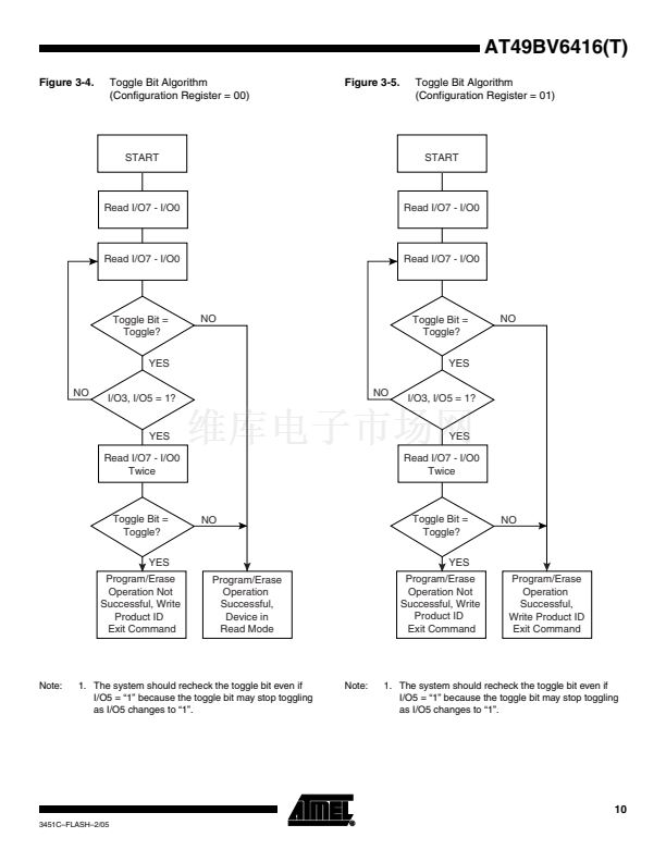
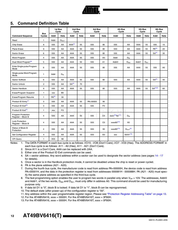
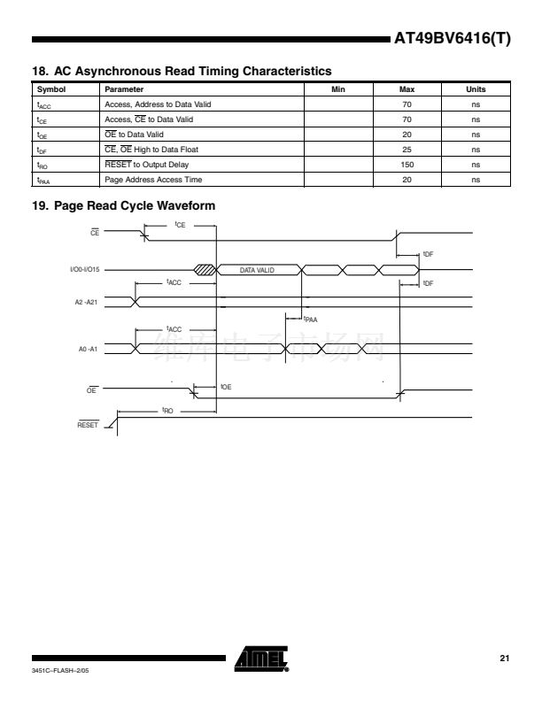
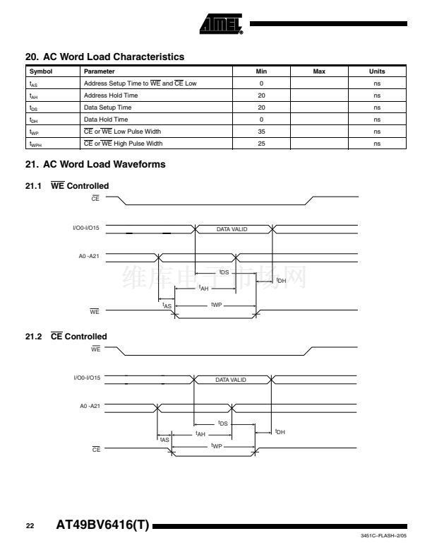
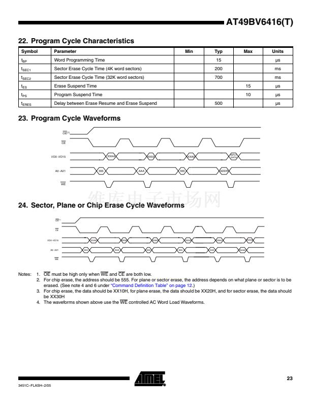
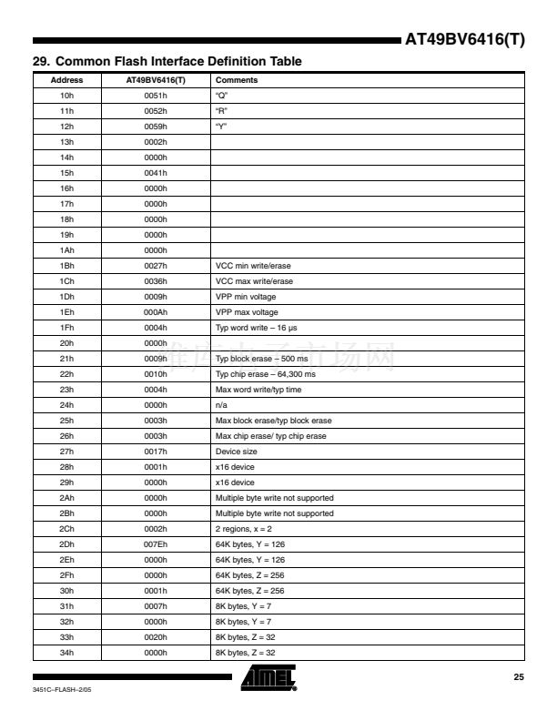
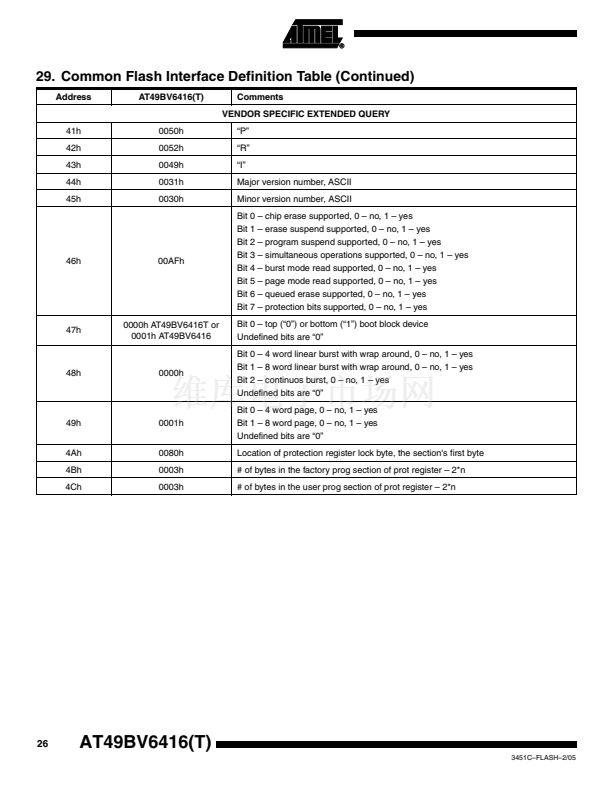
Figure 3-2.
Data Polling Algorithm
(Configuration Register = 00)
Figure 3-3.
Data Polling Algorithm
(Configuration Register = 01)
START
START
Read I/O7 - I/O0
Addr = VA
Read I/O7 - I/O0
Addr = VA
YES
I/O7 = Data?
NO
NO
NO
I/O7 = 1?
YES
NO
I/O3, I/O5 = 1?
I/O3, I/O5 = 1?
YES
Read I/O7 - I/O0
Addr = VA
YES
Program/Erase
Operation Not
Successful, Write
Product ID
Exit Command
Program/Erase
Operation
Successful,
Write Product ID
Exit Command
I/O7 = Data?
YES
NO
Program/Erase
Operation Not
Successful, Write
Product ID
Exit Command
Program/Erase
Operation
Successful,
Device in
Read Mode
Note:
1. VA = Valid address for programming. During a sector
erase operation, a valid address is any sector
address within the sector being erased. During chip
erase, a valid address is any non-protected sector
address.
Notes:
1. VA = Valid address for programming. During a sector
erase operation, a valid address is any sector
address within the sector being erased. During chip
erase, a valid address is any non-protected sector
address.
2. I/O7 should be rechecked even if I/O5 = 鈥?鈥?because
I/O7 may change simultaneously with I/O5.
9
AT49BV6416(T)
3451C鈥揊LASH鈥?/05


 1
1
 2
2
 3
3
 4
4
 5
5
 6
6
 7
7
 8
8
 9
9
 10
10
 11
11
 12
12
 13
13
 14
14
 15
15
 16
16
 17
17
 18
18
 19
19
 20
20
 21
21
 22
22
 23
23
 24
24
 25
25
 26
26
 27
27
 28
28
 29
29
 30
30
