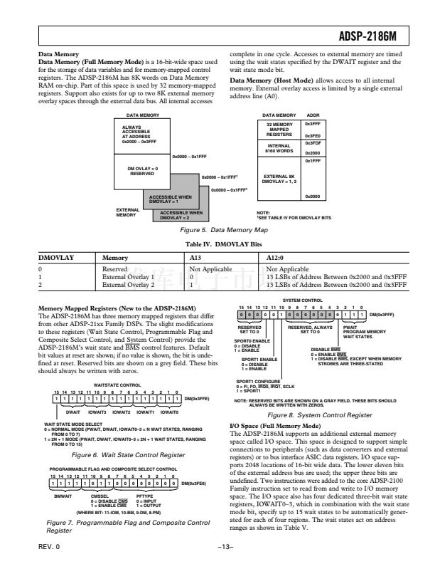
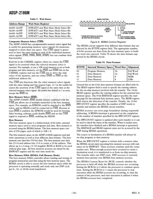
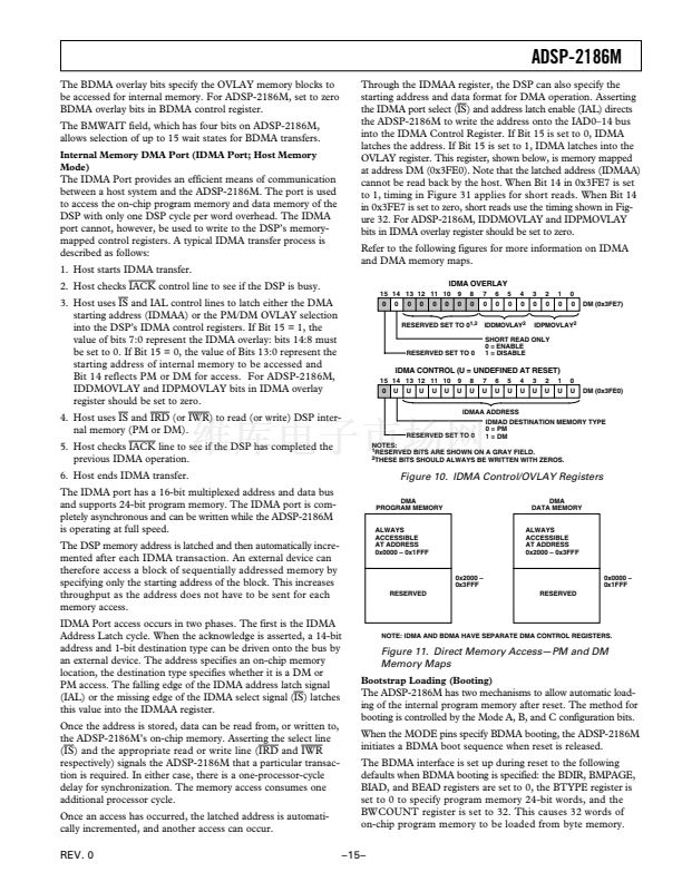
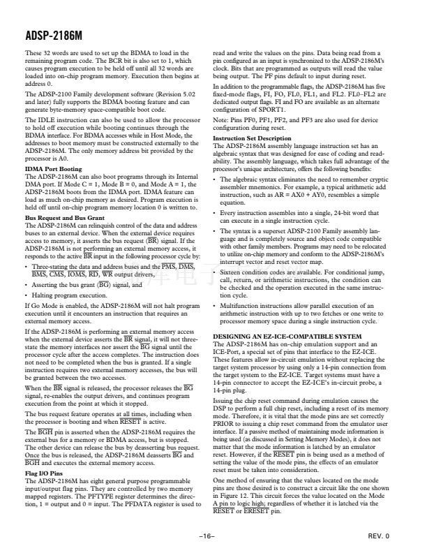
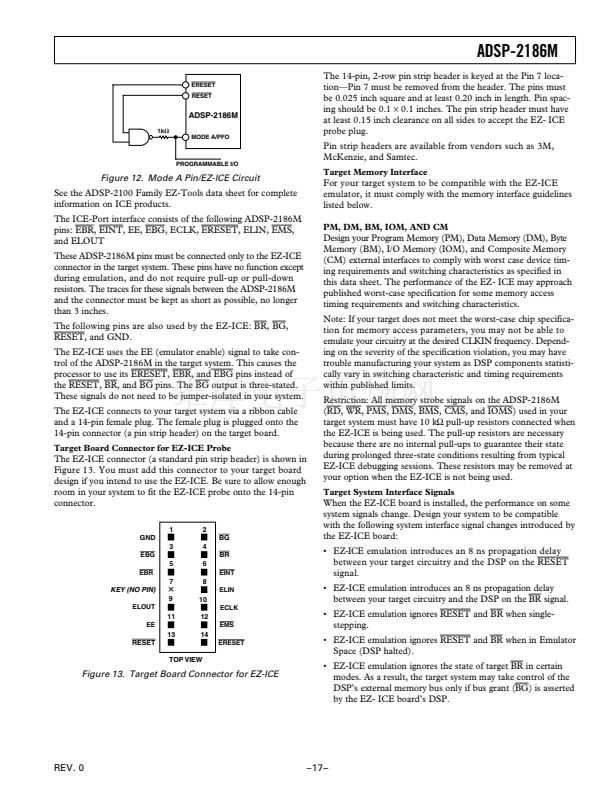
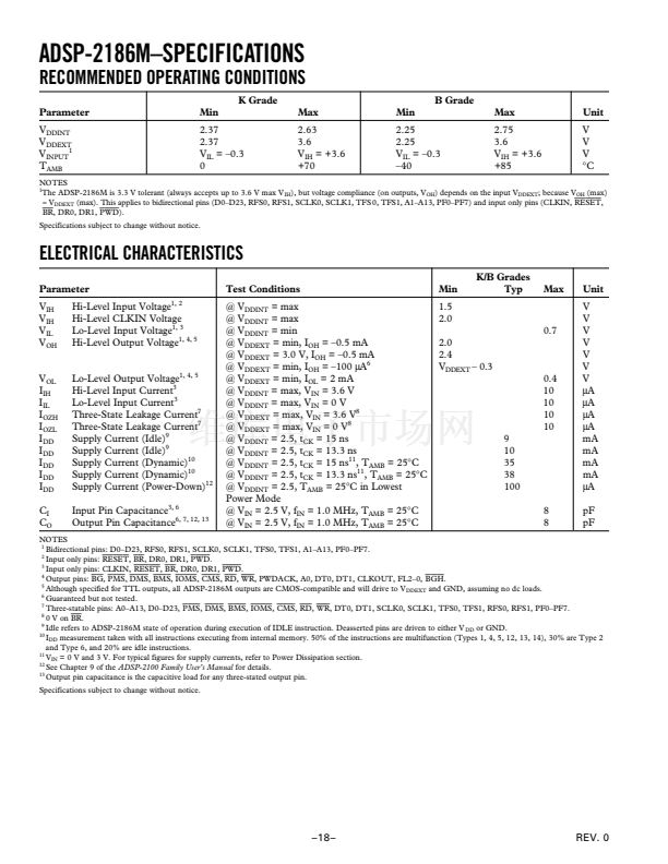
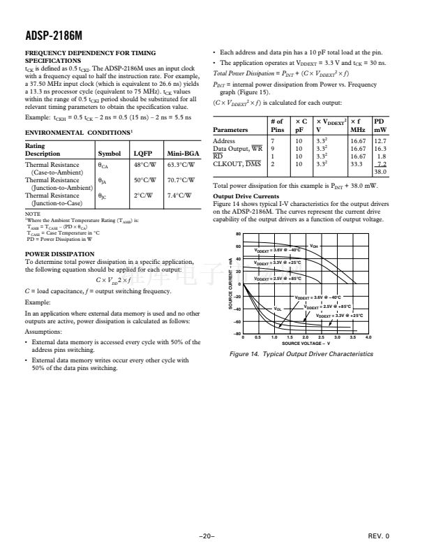
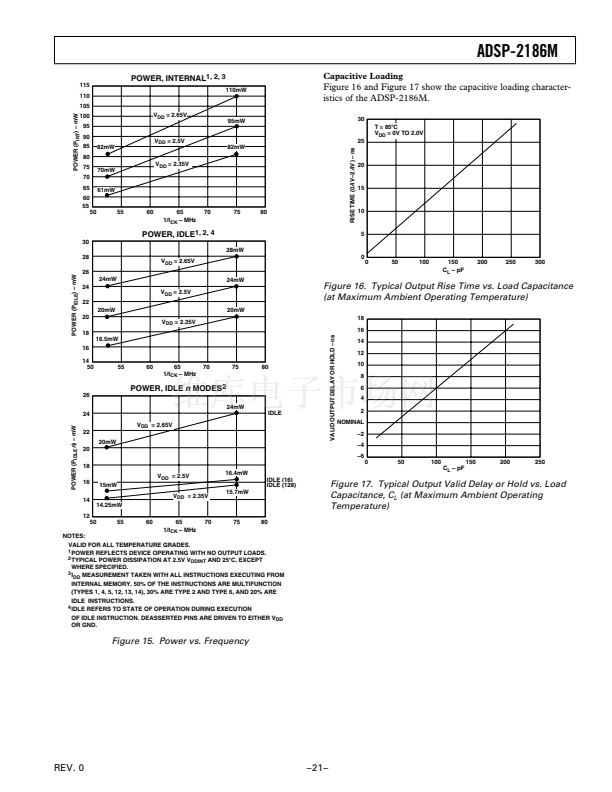
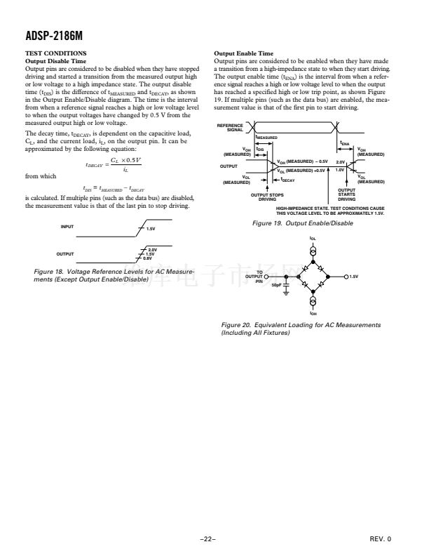
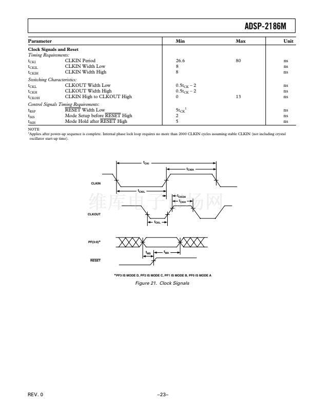
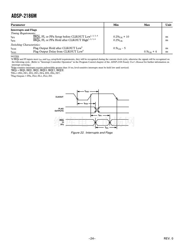
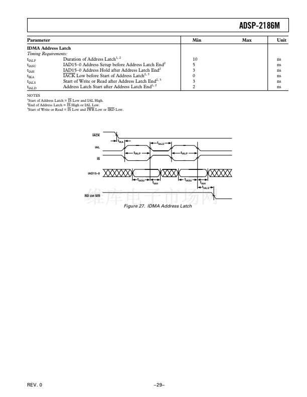
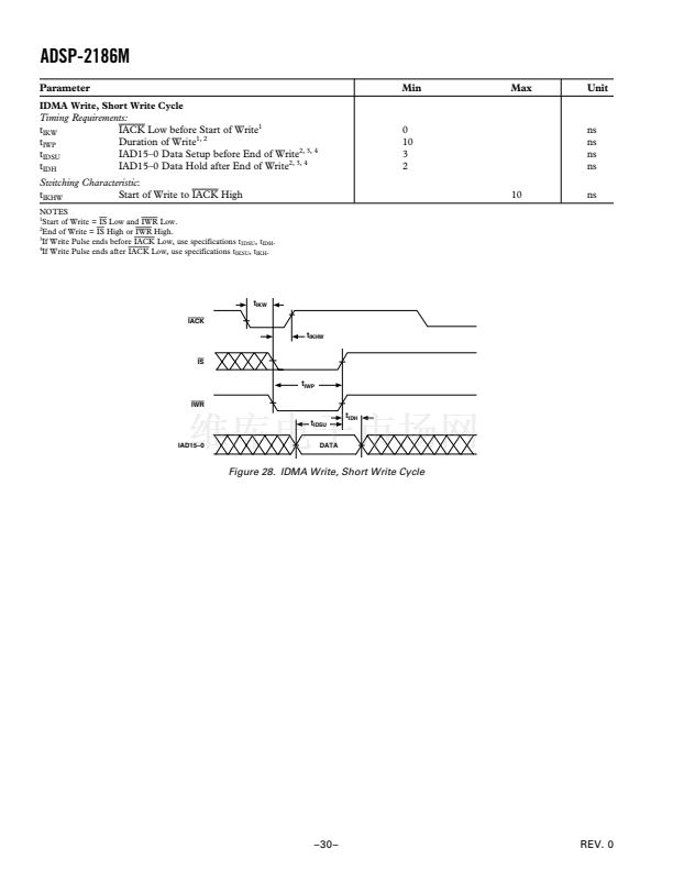
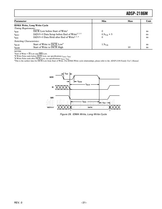
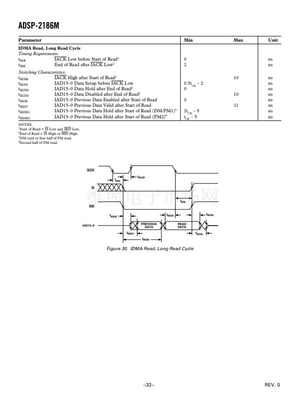
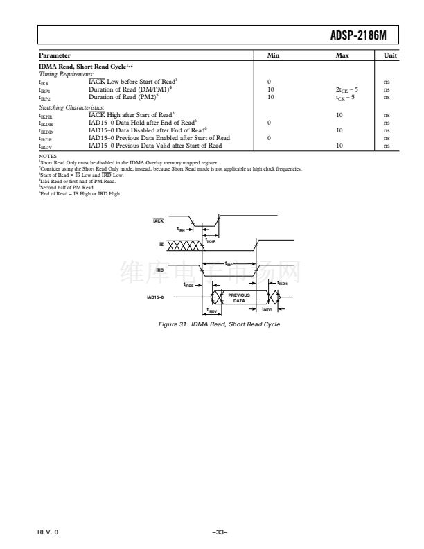
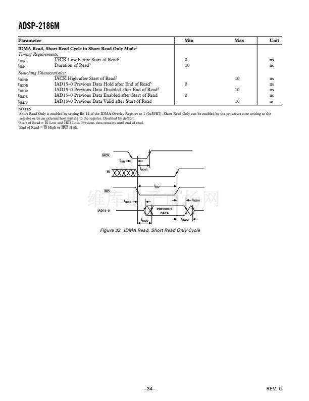
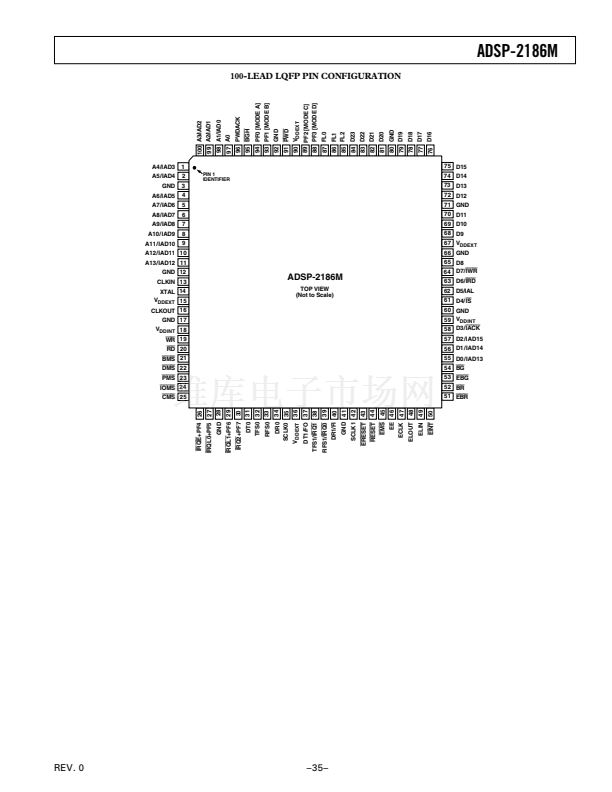
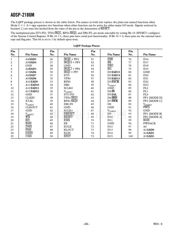
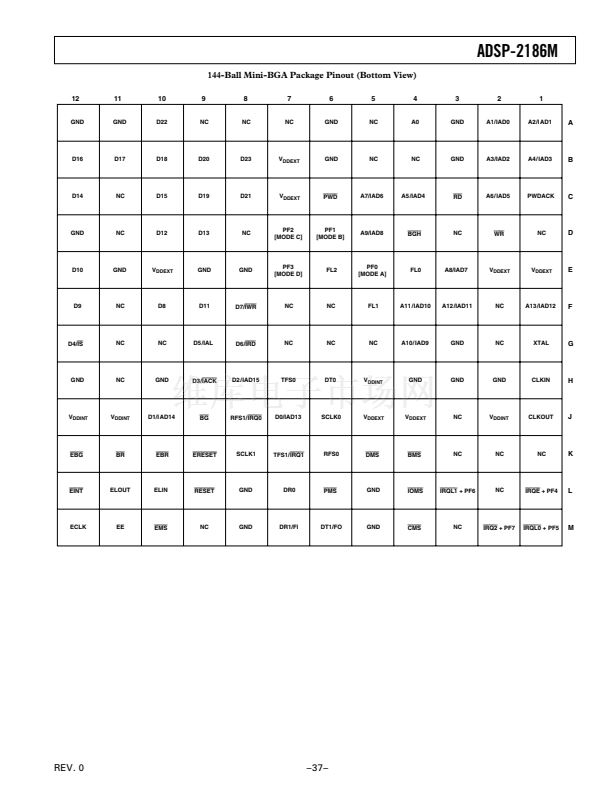
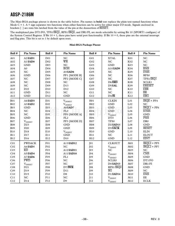
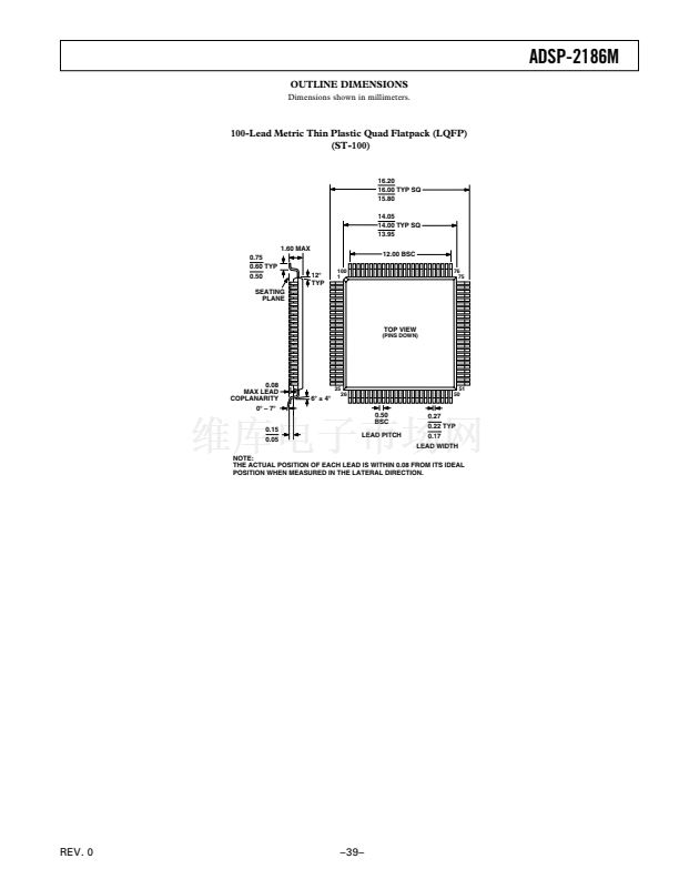
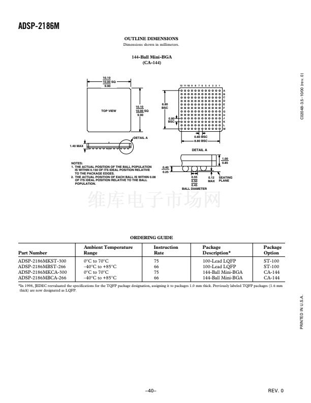
ADSP-2186M
Slow Idle
The IDLE instruction is enhanced on the ADSP-2186M to let
the processor鈥檚 internal clock signal be slowed, further reducing
power consumption. The reduced clock frequency, a program-
mable fraction of the normal clock rate, is specified by a selectable
divisor given in the IDLE instruction.
The format of the instruction is:
IDLE (n);
where
n
= 16, 32, 64, or 128. This instruction keeps the proces-
sor fully functional, but operating at the slower clock rate. While
it is in this state, the processor鈥檚 other internal clock signals, such
as SCLK, CLKOUT, and timer clock, are reduced by the same
ratio. The default form of the instruction, when no clock divisor
is given, is the standard IDLE instruction.
When the IDLE (n) instruction is used, it effectively slows down
the processor鈥檚 internal clock and thus its response time to incom-
ing interrupts. The one-cycle response time of the standard idle
state is increased by n, the clock divisor. When an enabled inter-
rupt is received, the ADSP-2186M will remain in the idle state
for up to a maximum of n processor cycles (n = 16, 32, 64, or
128) before resuming normal operation.
When the IDLE (n) instruction is used in systems that have an
externally generated serial clock (SCLK), the serial clock rate
may be faster than the processor鈥檚 reduced internal clock rate.
Under these conditions, interrupts must not be generated at a
faster than can be serviced, due to the additional time the
processor takes to come out of the idle state (a maximum of n
processor cycles).
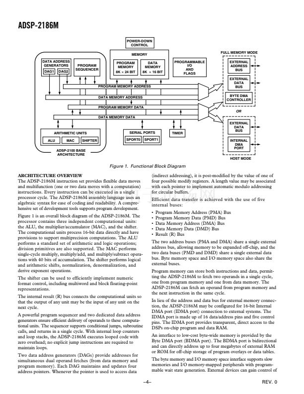
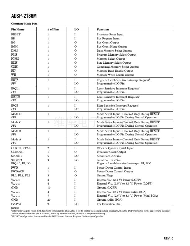
SYSTEM INTERFACE
ADSP-2186M also provides four external interrupts and two
serial ports or six external interrupts and one serial port. Host
Memory Mode allows access to the full external data bus, but
limits addressing to a single address bit (A0). Through the use
of external hardware, additional system peripherals can be added
in this mode to generate and latch address signals.
Clock Signals
The ADSP-2186M can be clocked by either a crystal or a
TTL-compatible clock signal.
The CLKIN input cannot be halted, changed during opera-
tion, nor operated below the specified frequency during normal
operation. The only exception is while the processor is in the
power-down state. For additional information, refer to Chap-
ter 9,
ADSP-2100 Family User鈥檚 Manual,
for detailed information
on this power-down feature.
If an external clock is used, it should be a TTL-compatible signal
running at half the instruction rate. The signal is connected to
the processor鈥檚 CLKIN input. When an external clock is used,
the XTAL input must be left unconnected.
The ADSP-2186M uses an input clock with a frequency equal to
half the instruction rate; a 37.50 MHz input clock yields a 13 ns
processor cycle (which is equivalent to 75 MHz). Normally,
instructions are executed in a single processor cycle. All device
timing is relative to the internal instruction clock rate, which is
indicated by the CLKOUT signal when enabled.
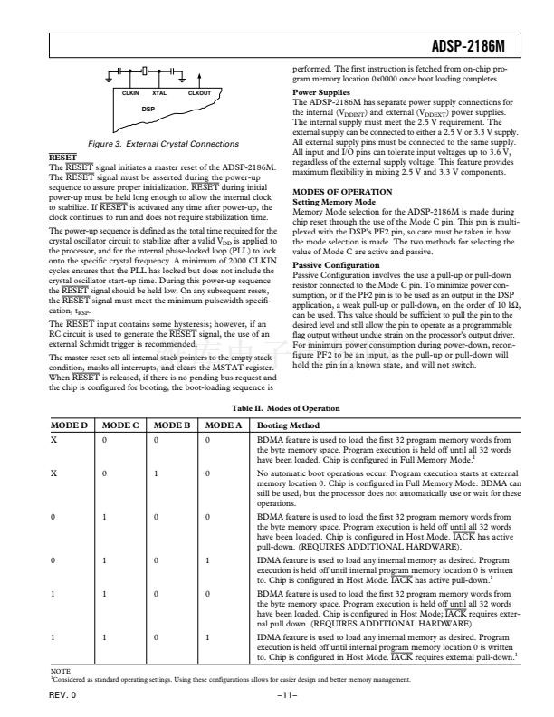
Because the ADSP-2186M includes an on-chip oscillator circuit,
an external crystal may be used. The crystal should be connected
across the CLKIN and XTAL pins, with two capacitors con-
nected as shown in Figure 3. Capacitor values are dependent on
crystal type and should be specified by the crystal manufacturer.
A parallel-resonant, fundamental frequency, microprocessor-
grade crystal should be used.
A clock output (CLKOUT) signal is generated by the processor
at the processor鈥檚 cycle rate. This can be enabled and disabled by
the CLKODIS bit in the SPORT0 Autobuffer Control Register.
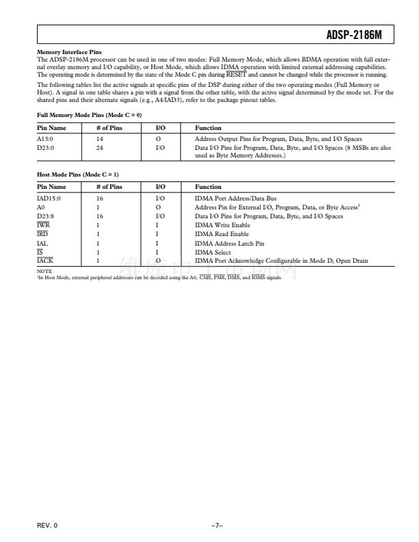
HOST MEMORY MODE
ADSP-2186M
1/2x CLOCK
OR
CRYSTAL
CLKIN
XTAL
FL0鈥?
BYTE
MEMORY
A0
16
1
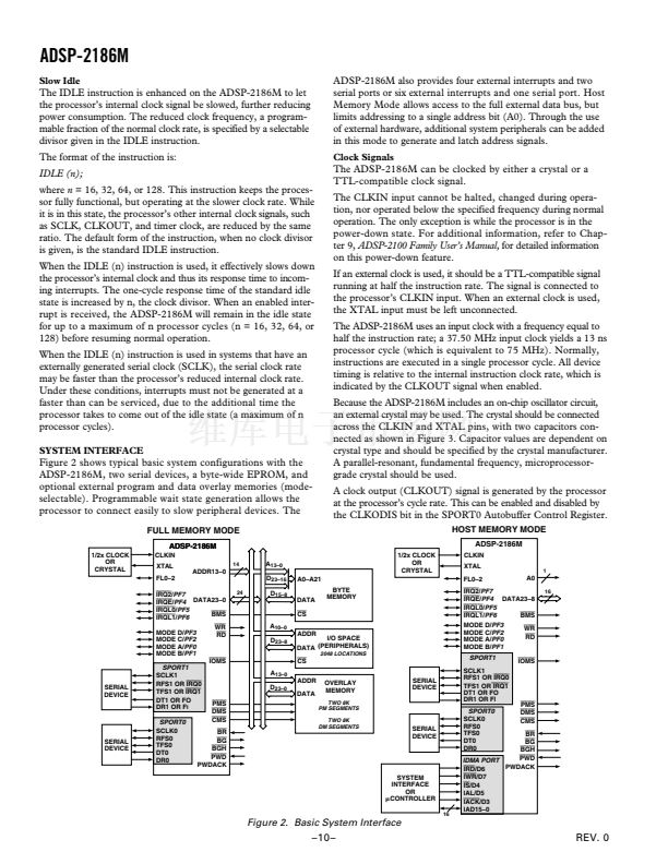
Figure 2 shows typical basic system configurations with the
ADSP-2186M, two serial devices, a byte-wide EPROM, and
optional external program and data overlay memories (mode-
selectable). Programmable wait state generation allows the
processor to connect easily to slow peripheral devices. The
FULL MEMORY MODE
ADSP-2186M
1/2x CLOCK
OR
CRYSTAL
CLKIN
XTAL
FL0鈥?
IRQ2/PF7
IRQE/PF4
DATA23鈥?
IRQL0/PF5
BMS
IRQL1/PF6
WR
MODE D/PF3
RD
MODE C/PF2
MODE A/PF0
MODE B/PF1
IOMS
SPORT1
SCLK1
RFS1 OR
IRQ0
TFS1 OR
IRQ1
DT1 OR FO
PMS
DR1 OR F
I
DMS
CMS
SPORT0
SCLK0
RFS0
TFS0
DT0
DR0
BR
BG
BGH
PWD
PWDACK
24
14
A
13鈥?
D
23鈥?6
D
15鈥?
A0鈥揂21
DATA
CS
A
10鈥?
D
23鈥?
I/O SPACE
DATA (PERIPHERALS)
2048 LOCATIONS
ADDR13鈥?
ADDR
IRQ2/PF7
IRQE/PF4
DATA23鈥?
IRQL0/PF5
IRQL1/PF6
BMS
MODE D/PF3
WR
MODE C/PF2
RD
MODE A/PF0
MODE B/PF1
SPORT1
SCLK1
RFS1 OR
IRQ0
TFS1 OR
IRQ1
DT1 OR FO
DR1 OR FI
SPORT0
SCLK0
RFS0
TFS0
DT0
DR0
IOMS
CS
A
13鈥?
ADDR
D
23鈥?
DATA
OVERLAY
MEMORY
TWO 8K
PM SEGMENTS
TWO 8K
DM SEGMENTS
SERIAL
DEVICE
SERIAL
DEVICE
PMS
DMS
CMS
SERIAL
DEVICE
SERIAL
DEVICE
SYSTEM
INTERFACE
OR
CONTROLLER
16
BR
BG
BGH
PWD
IDMA PORT
PWDACK
IRD/D6
IWR/D7
IS/D4
IAL/D5
IACK/D3
IAD15鈥?
Figure 2. Basic System Interface
prev
next


 1
1
 2
2
 3
3
 4
4
 5
5
 6
6
 7
7
 8
8
 9
9
 10
10
 11
11
 12
12
 13
13
 14
14
 15
15
 16
16
 17
17
 18
18
 19
19
 20
20
 21
21
 22
22
 23
23
 24
24
 25
25
 26
26
 27
27
 28
28
 29
29
 30
30
 31
31
 32
32
 33
33
 34
34
 35
35
 36
36
 37
37
 38
38
 39
39
 40
40
