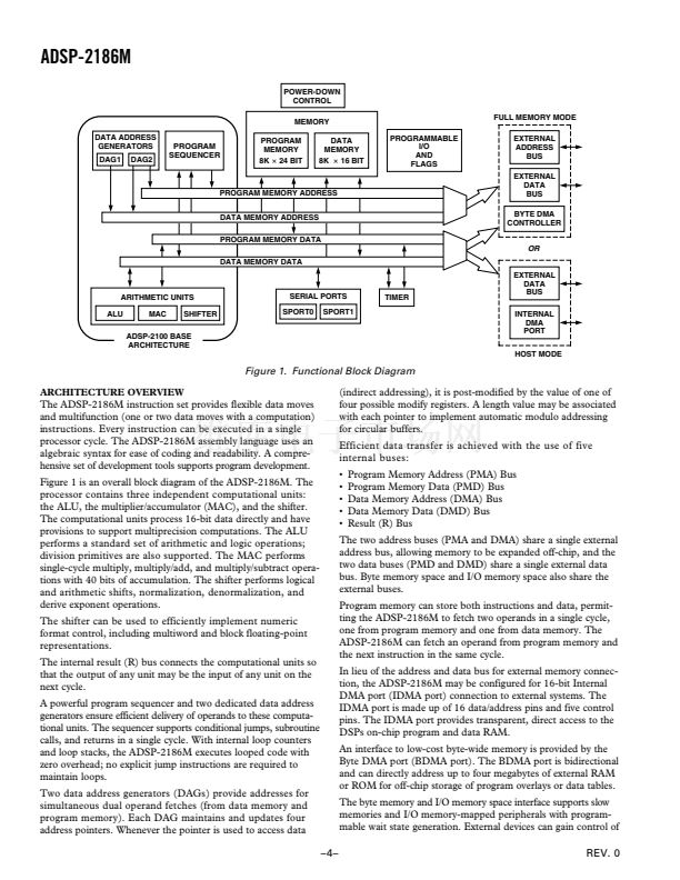
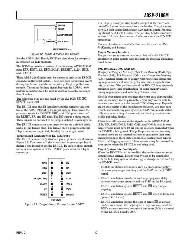
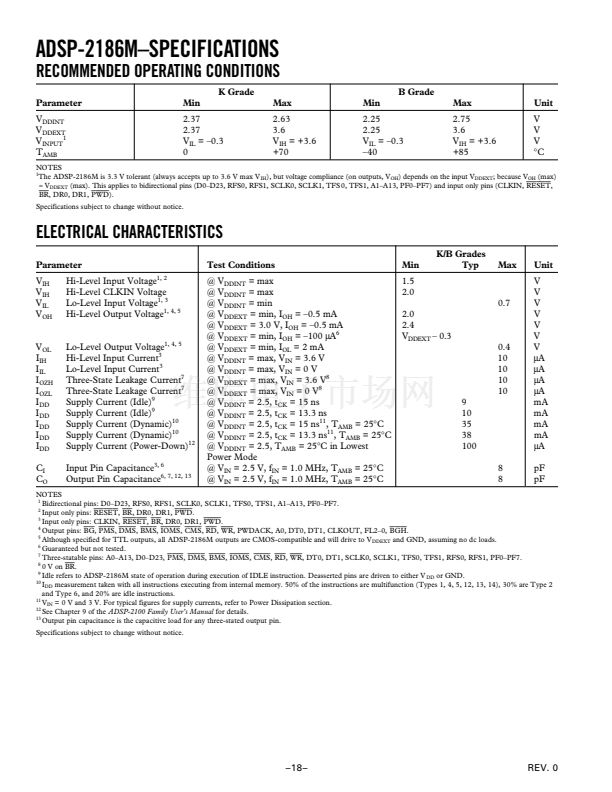
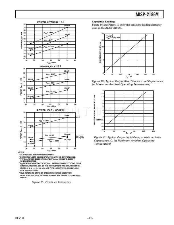
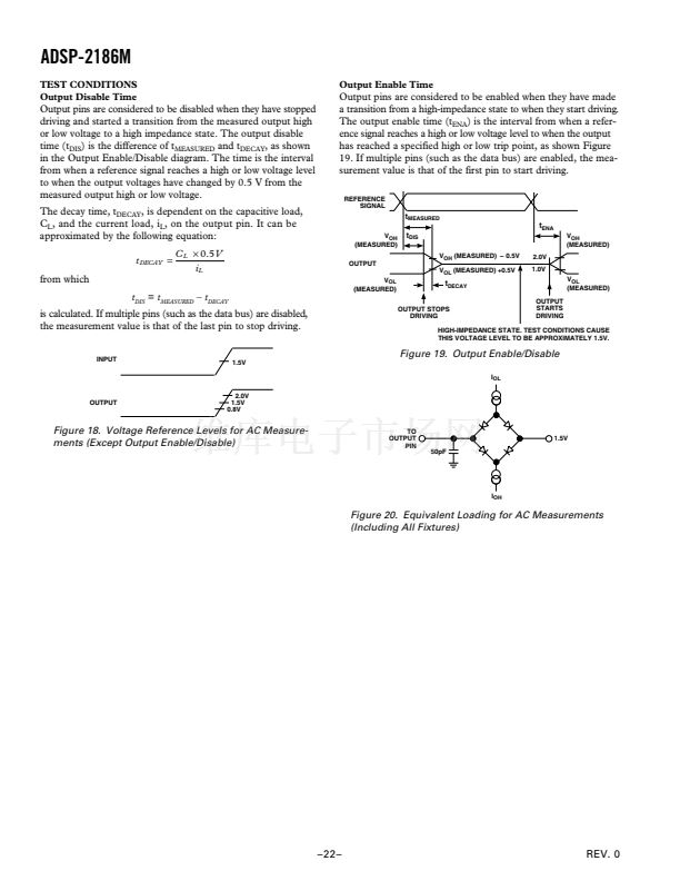
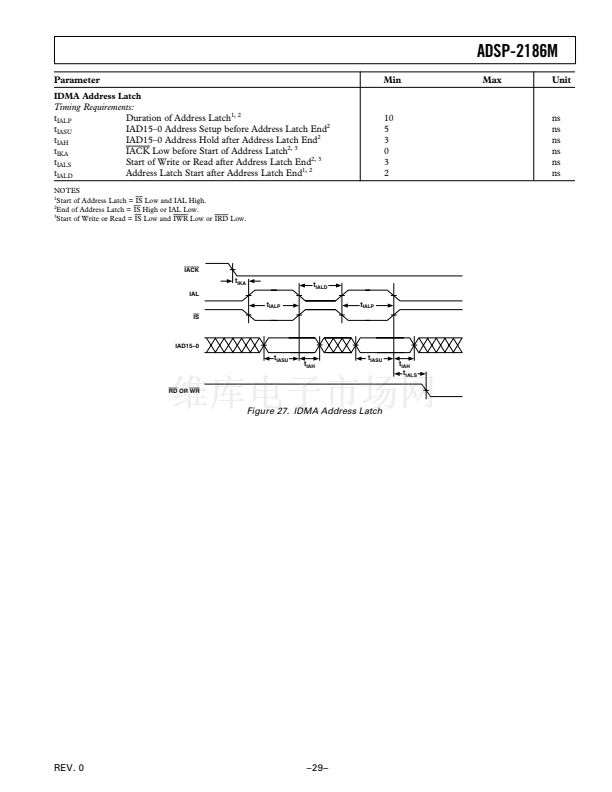
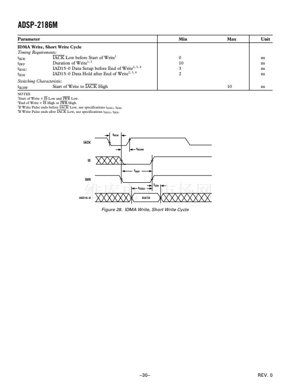
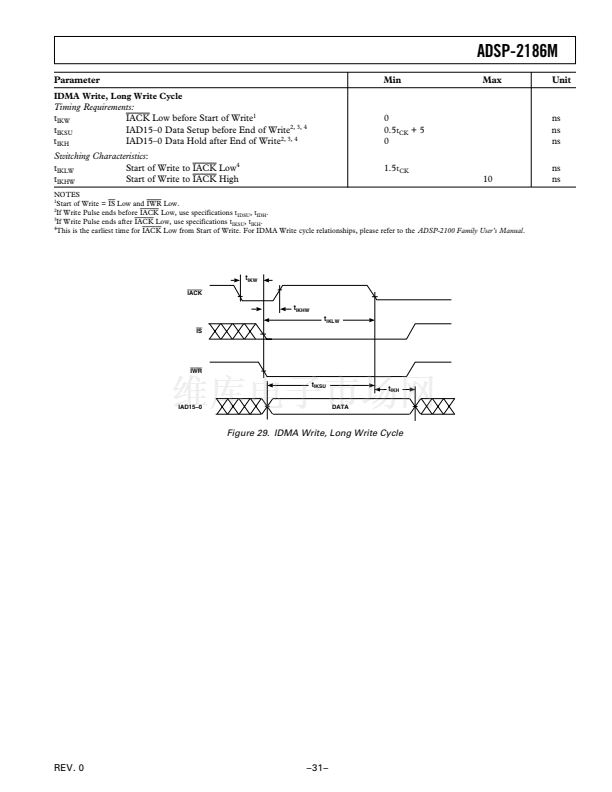
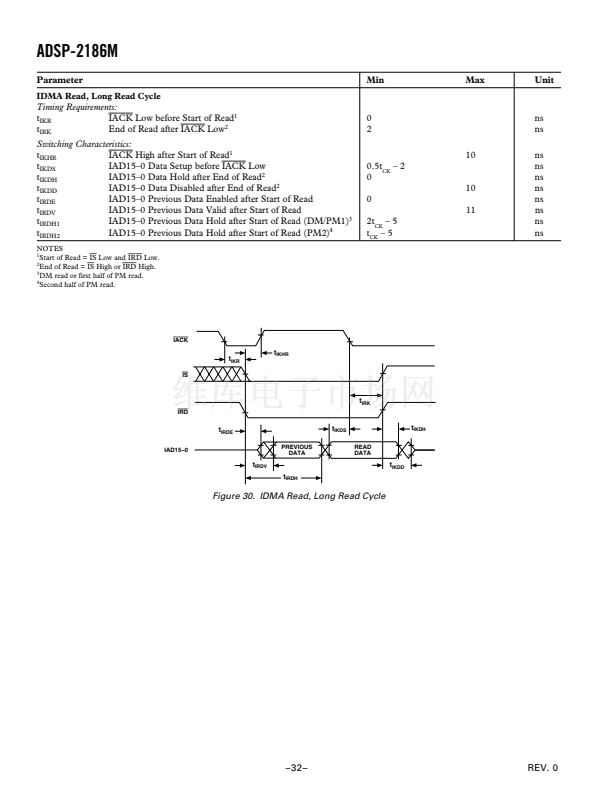
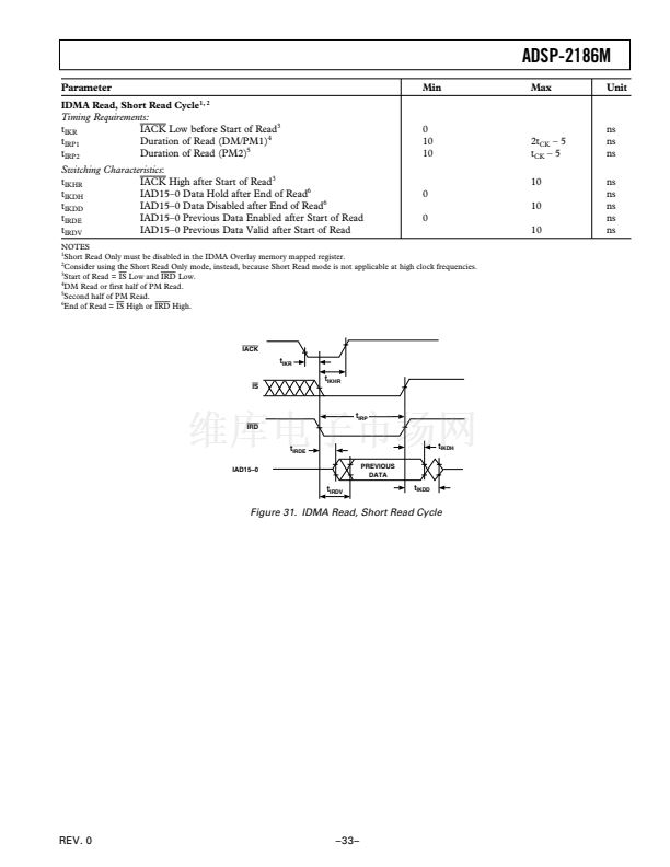
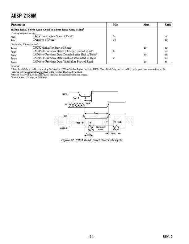
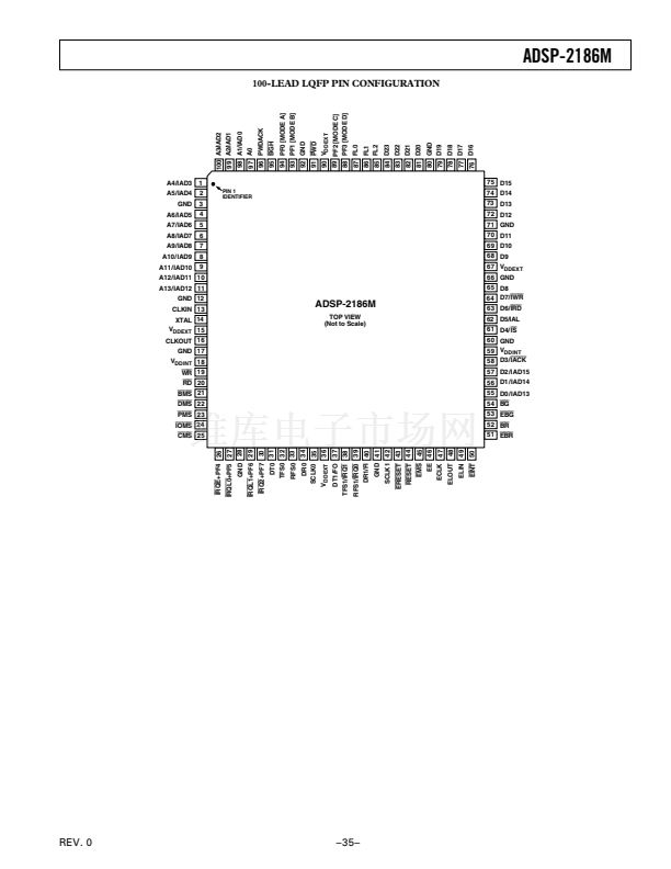
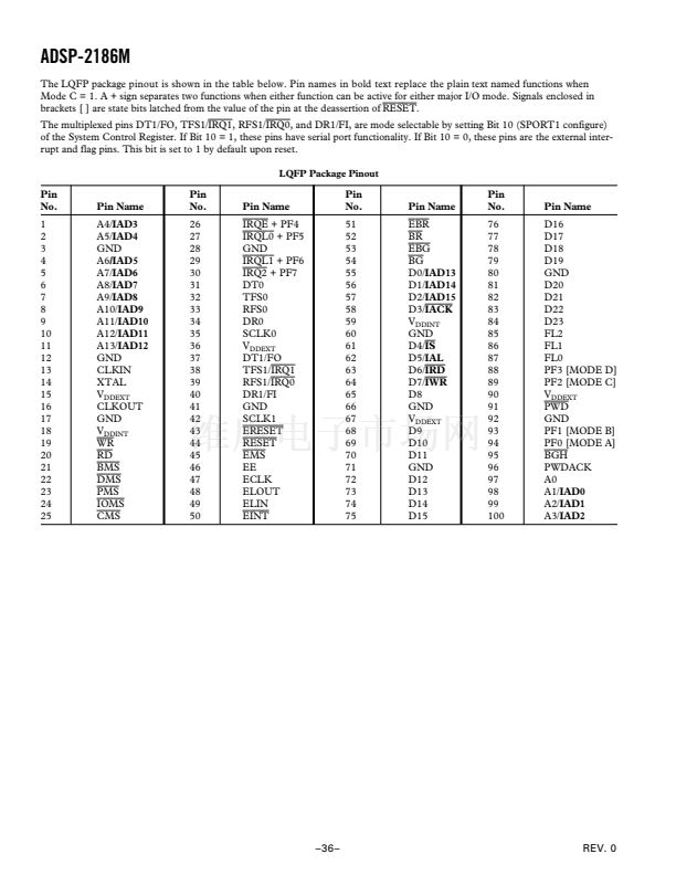
ADSP-2186M
TEST CONDITIONS
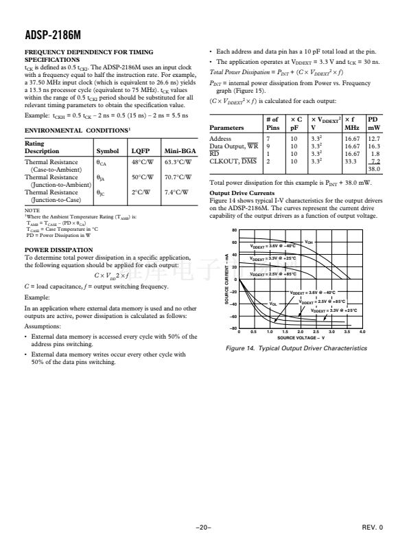
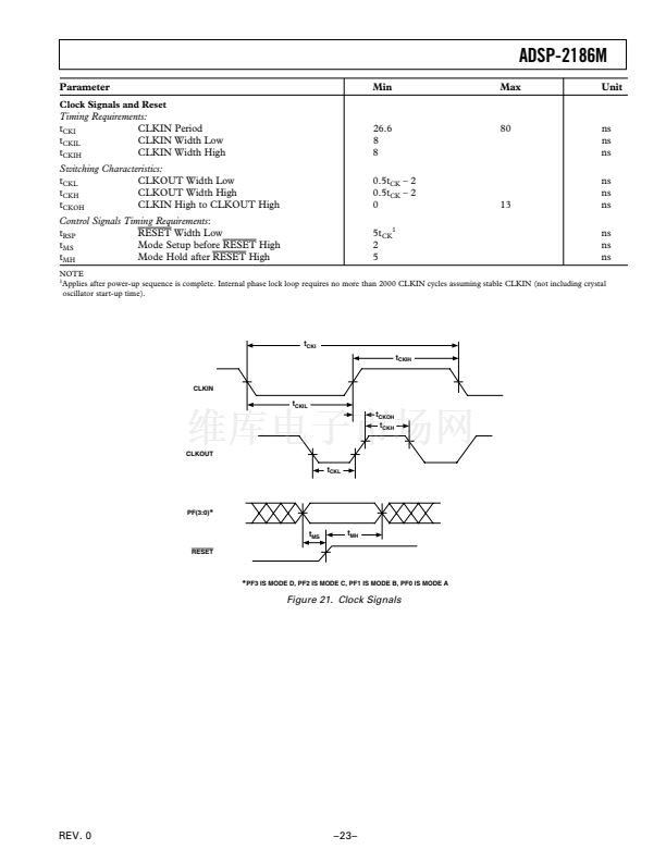
Output Disable Time
Output Enable Time
Output pins are considered to be disabled when they have stopped
driving and started a transition from the measured output high
or low voltage to a high impedance state. The output disable
time (t
DIS
) is the difference of t
MEASURED
and t
DECAY
, as shown
in the Output Enable/Disable diagram. The time is the interval
from when a reference signal reaches a high or low voltage level
to when the output voltages have changed by 0.5 V from the
measured output high or low voltage.
The decay time, t
DECAY
, is dependent on the capacitive load,
C
L
, and the current load, i
L
, on the output pin. It can be
approximated by the following equation:
t
DECAY
=
C
L
脳
0.5
V
i
L
Output pins are considered to be enabled when they have made
a transition from a high-impedance state to when they start driving.
The output enable time (t
ENA
) is the interval from when a refer-
ence signal reaches a high or low voltage level to when the output
has reached a specified high or low trip point, as shown Figure
19. If multiple pins (such as the data bus) are enabled, the mea-
surement value is that of the first pin to start driving.
REFERENCE
SIGNAL
t
MEASURED
t
ENA
V
OH
(MEASURED)
OUTPUT
V
OL
(MEASURED) +0.5V
V
OL
(MEASURED)
t
DIS
V
OH
(MEASURED) 鈥?0.5V
2.0V
1.0V
V
OH
(MEASURED)
from which
t
DIS
=
t
MEASURED
鈥?/div>
t
DECAY
is calculated. If multiple pins (such as the data bus) are disabled,
the measurement value is that of the last pin to stop driving.
INPUT
t
DECAY
OUTPUT STOPS
DRIVING
OUTPUT
STARTS
DRIVING
V
OL
(MEASURED)
HIGH-IMPEDANCE STATE. TEST CONDITIONS CAUSE
THIS VOLTAGE LEVEL TO BE APPROXIMATELY 1.5V.
Figure 19. Output Enable/Disable
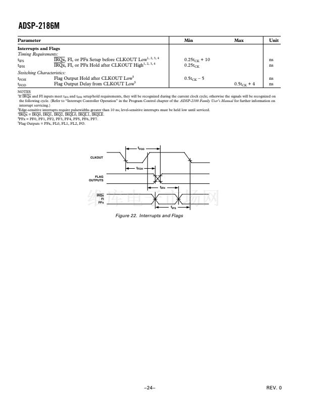
1.5V
I
OL
2.0V
1.5V
0.8V
TO
OUTPUT
PIN
50pF
OUTPUT
Figure 18. Voltage Reference Levels for AC Measure-
ments (Except Output Enable/Disable)
1.5V
I
OH
Figure 20. Equivalent Loading for AC Measurements
(Including All Fixtures)
prev
next


 1
1
 2
2
 3
3
 4
4
 5
5
 6
6
 7
7
 8
8
 9
9
 10
10
 11
11
 12
12
 13
13
 14
14
 15
15
 16
16
 17
17
 18
18
 19
19
 20
20
 21
21
 22
22
 23
23
 24
24
 25
25
 26
26
 27
27
 28
28
 29
29
 30
30
 31
31
 32
32
 33
33
 34
34
 35
35
 36
36
 37
37
 38
38
 39
39
 40
40
