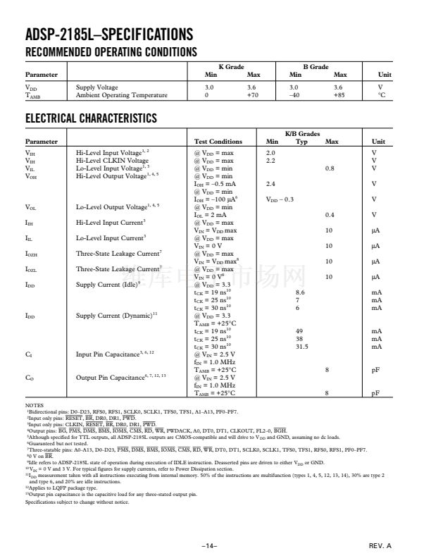
ADSP-2185L鈥揝PECIFICATIONS
RECOMMENDED OPERATING CONDITIONS
K Grade
Parameter
V
DD
T
AMB
Supply Voltage
Ambient Operating Temperature
Min
3.0
0
Max
3.6
+70
Min
3.0
鈥?0
B Grade
Max
3.6
+85
Unit
V
掳C
ELECTRICAL CHARACTERISTICS
Parameter
V
IH
V
IH
V
IL
V
OH
Hi-Level Input Voltage
1, 2
Hi-Level CLKIN Voltage
Lo-Level Input Voltage
1, 3
Hi-Level Output Voltage
1, 4, 5
Test Conditions
@ V
DD
= max
@ V
DD
= max
@ V
DD
= min
@ V
DD
= min
I
OH
= 鈥?.5 mA
@ V
DD
= min
I
OH
= 鈥?00
碌A
6
@ V
DD
= min
I
OL
= 2 mA
@ V
DD
= max
V
IN
= V
DD
max
@ V
DD
= max
V
IN
= 0 V
@ V
DD
= max
V
IN
= V
DD
max
8
@ V
DD
= max
V
IN
= 0 V
8
@ V
DD
= 3.3
t
CK
= 19 ns
10
t
CK
= 25 ns
10
t
CK
= 30 ns
10
@ V
DD
= 3.3
T
AMB
= +25掳C
t
CK
= 19 ns
10
t
CK
= 25 ns
10
t
CK
= 30 ns
10
@ V
IN
= 2.5 V
f
IN
= 1.0 MHz
T
AMB
= +25掳C
@ V
IN
= 2.5 V
f
IN
= 1.0 MHz
T
AMB
= +25掳C
Min
2.0
2.2
0.8
2.4
V
DD
鈥?0.3
0.4
10
10
10
10
8.6
7
6
K/B Grades
Typ
Max
Unit
V
V
V
V
V
V
碌A
碌A
碌A
碌A
mA
mA
mA
V
OL
I
IH
I
IL
I
OZH
I
OZL
I
DD
Lo-Level Output Voltage
Hi-Level Input Current
3
1, 4, 5
Lo-Level Input Current
3
Three-State Leakage Current
7
Three-State Leakage Current
Supply Current (Idle)
9
7
I
DD
Supply Current (Dynamic)
11
49
38
31.5
mA
mA
mA
C
I
Input Pin Capacitance
3, 6, 12
6, 7, 12, 13
8
pF
C
O
Output Pin Capacitance
8
pF
NOTES
11
Bidirectional pins: D0鈥揇23, RFS0, RFS1, SCLK0, SCLK1, TFS0, TFS1, A1鈥揂13, PF0鈥揚F7.
12
Input only pins:
RESET, BR,
DR0, DR1,
PWD.
13
Input only pins: CLKIN,
RESET, BR,
DR0, DR1,
PWD.
14
Output pins:
BG, PMS, DMS, BMS, IOMS, CMS, RD, WR,
PWDACK, A0, DT0, DT1, CLKOUT, FL2鈥?,
BGH.
15
Although specified for TTL outputs, all ADSP-2185L outputs are CMOS-compatible and will drive to V
DD
and GND, assuming no dc loads.
16
Guaranteed but not tested.
17
Three-statable pins: A0鈥揂13, D0鈥揇23,
PMS, DMS, BMS, IOMS, CMS, RD, WR,
DT0, DT1, SCLK0, SCLK1, TFS0, TFS1, RFS0, RFS1, PF0鈥揚F7.
18
0 V on
BR.
19
Idle refers to ADSP-2185L state of operation during execution of IDLE instruction. Deasserted pins are driven to either V
DD
or GND.
10
V
IN
= 0 V and 3 V. For typical figures for supply currents, refer to Power Dissipation section.
11
I
DD
measurement taken with all instructions executing from internal memory. 50% of the instructions are multifunction (types 1, 4, 5, 12, 13, 14), 30% are type 2
and type 6, and 20% are idle instructions.
12
Applies to LQFP package type.
13
Output pin capacitance is the capacitive load for any three-stated output pin.
Specifications subject to change without notice.
prev
next


 1
1
 2
2
 3
3
 4
4
 5
5
 6
6
 7
7
 8
8
 9
9
 10
10
 11
11
 12
12
 13
13
 14
14
 15
15
 16
16
 17
17
 18
18
 19
19
 20
20
 21
21
 22
22
 23
23
 24
24
 25
25
 26
26
 27
27
 28
28
 29
29
 30
30
 31
31
