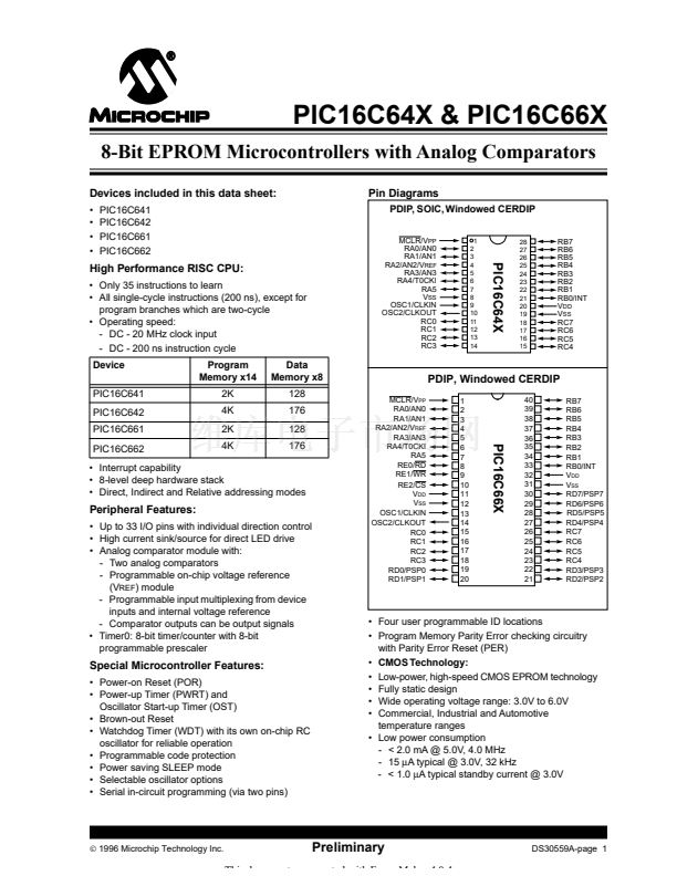
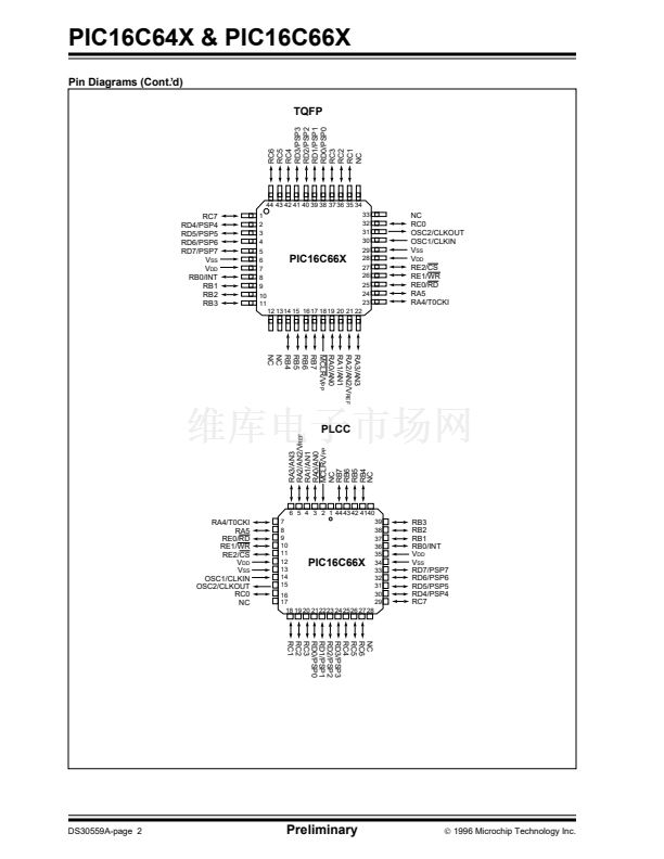
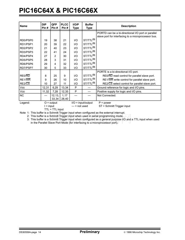
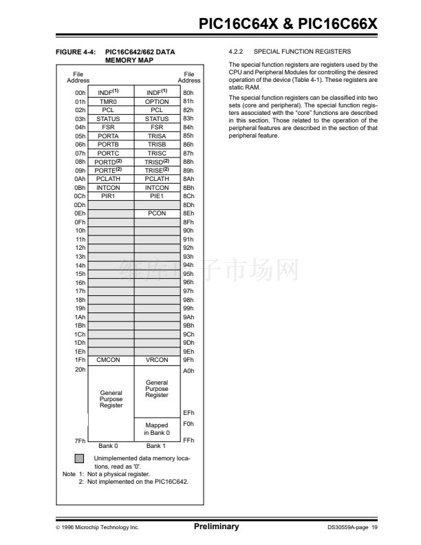
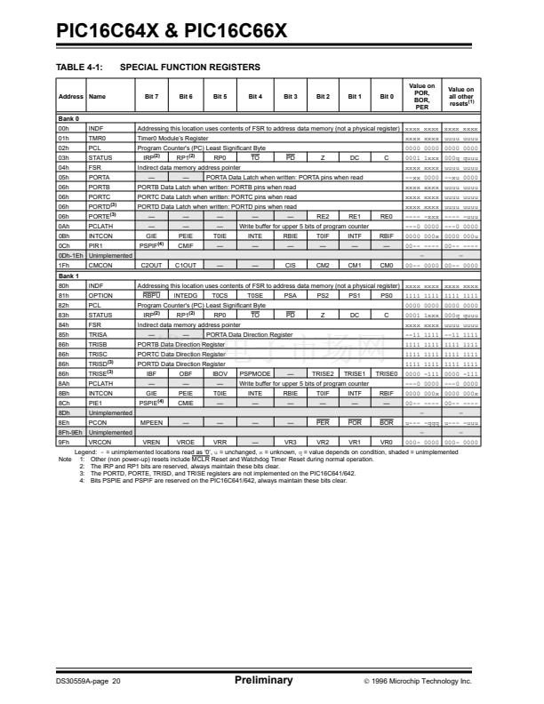
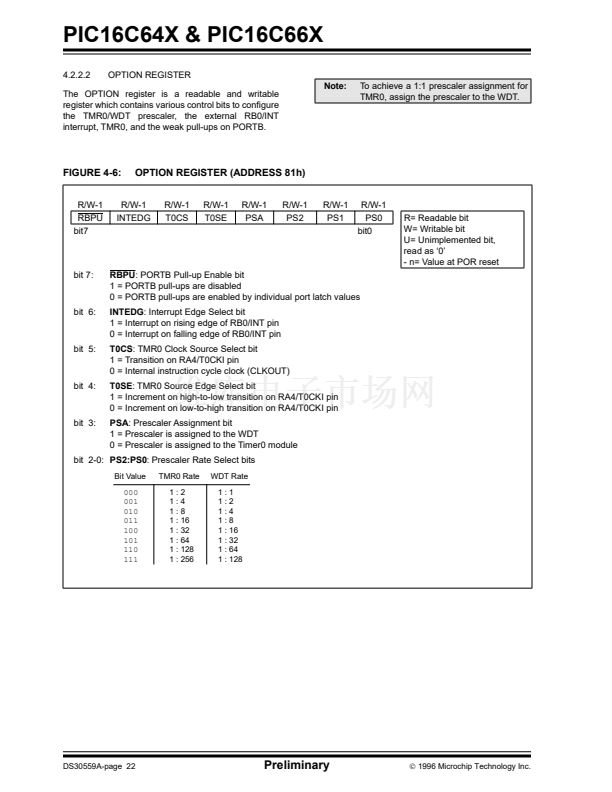
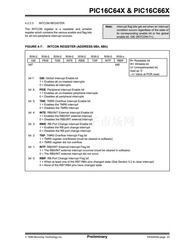
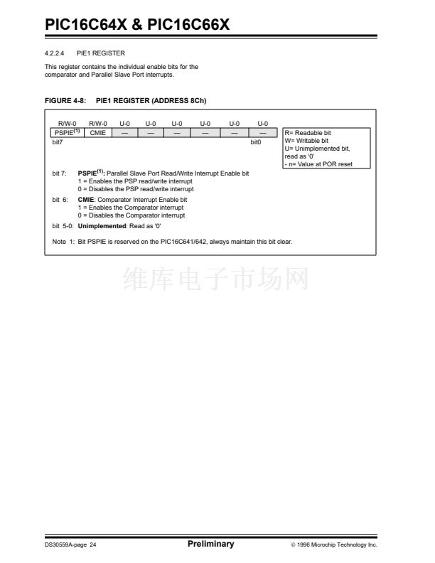
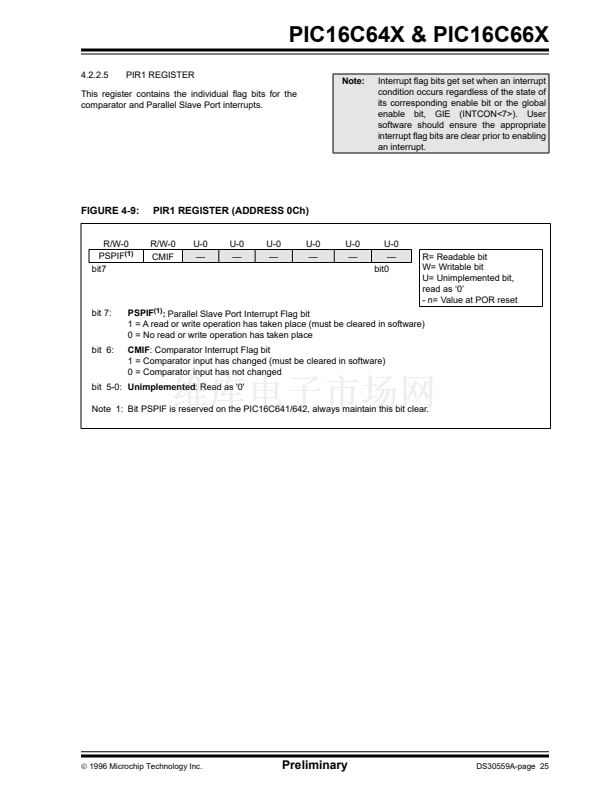
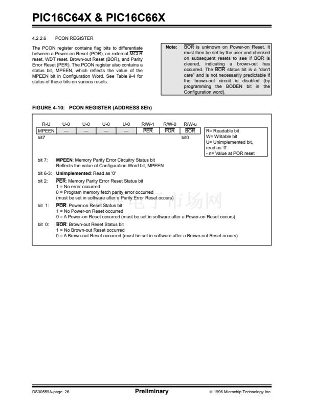
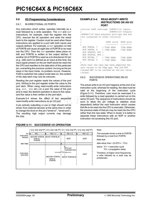
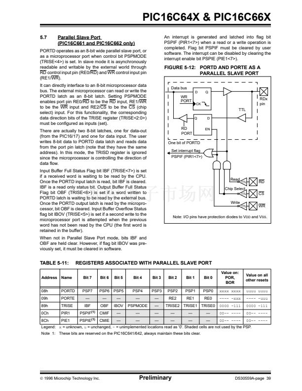
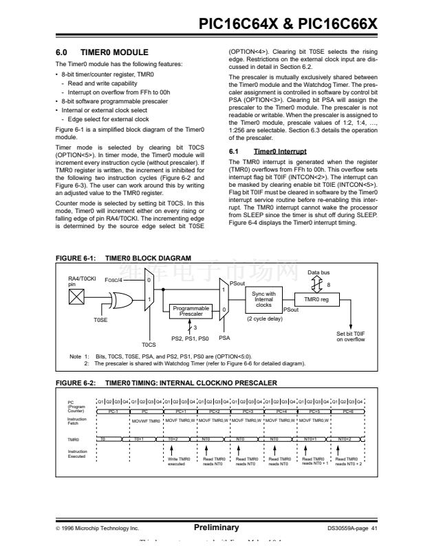
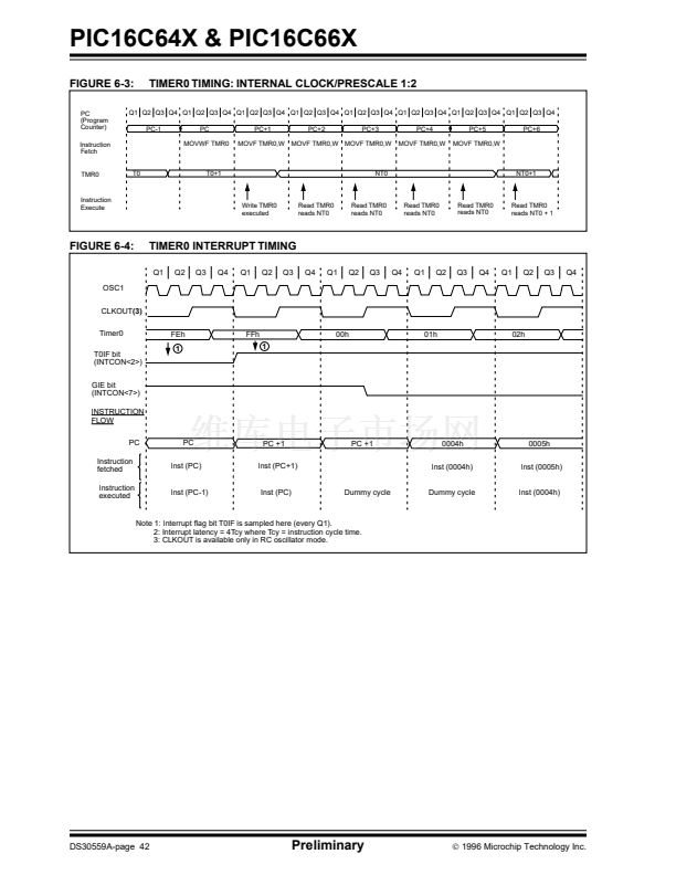
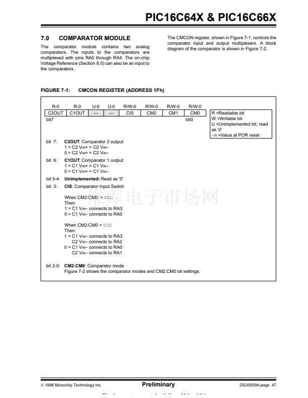
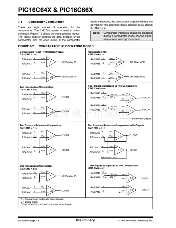
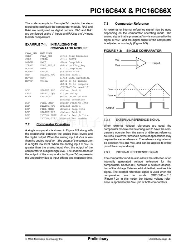
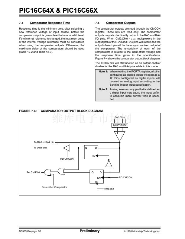
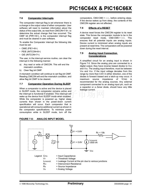
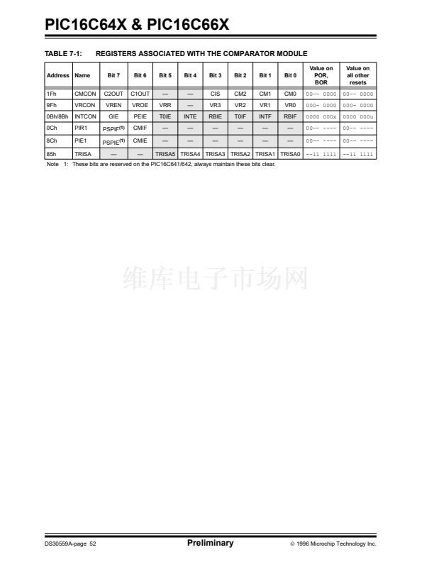
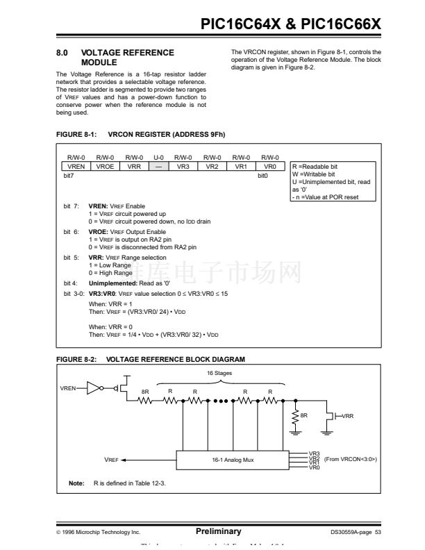
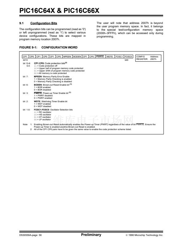
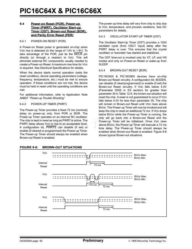
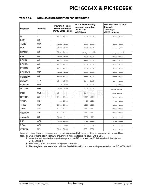
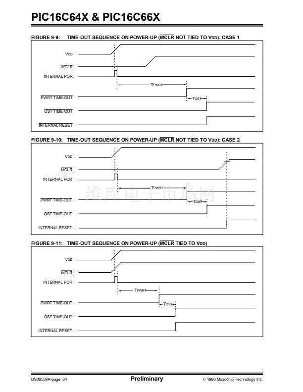
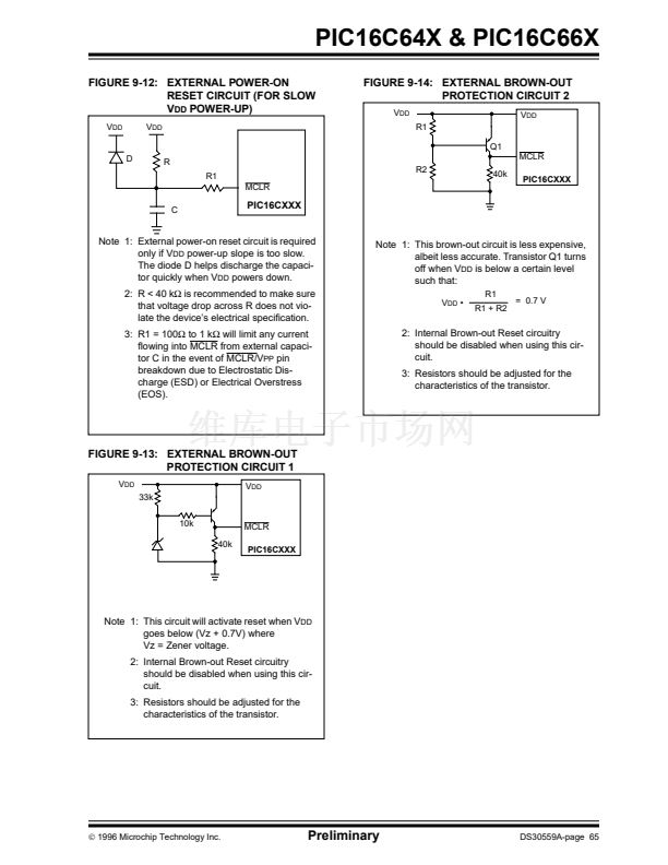
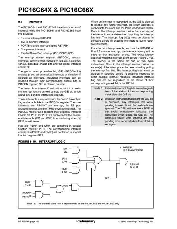
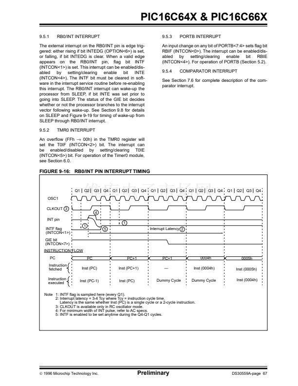
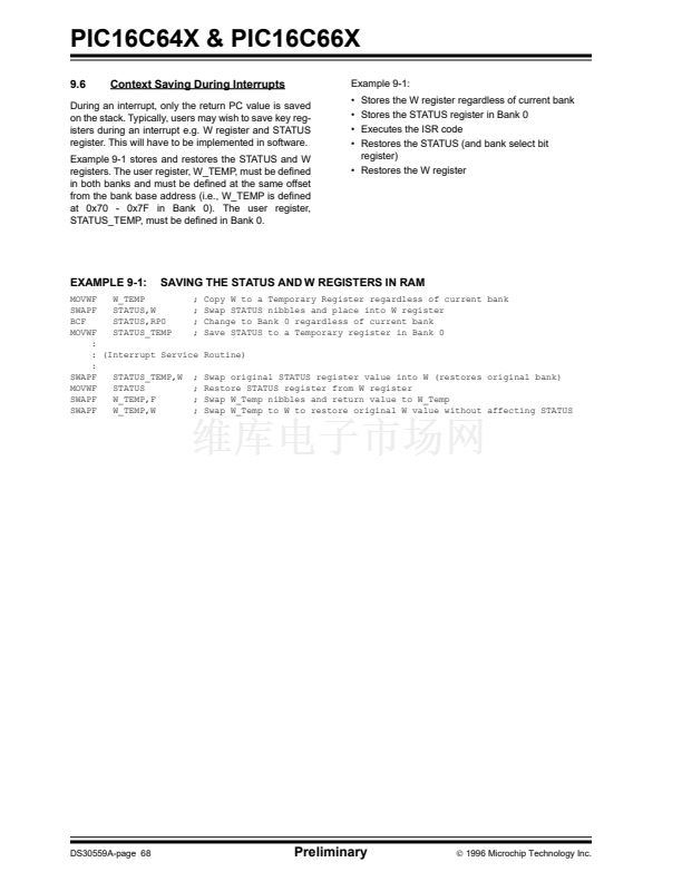
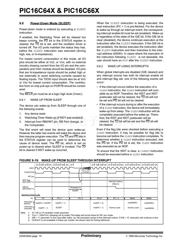
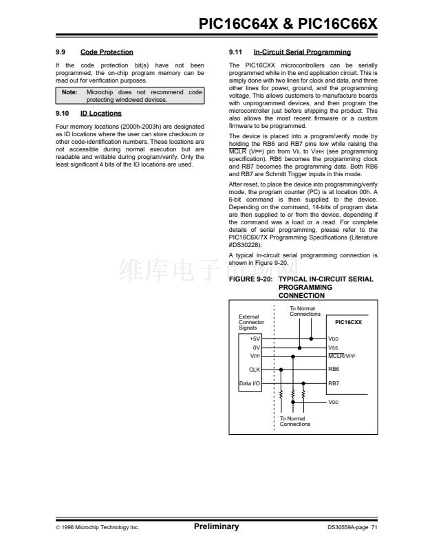
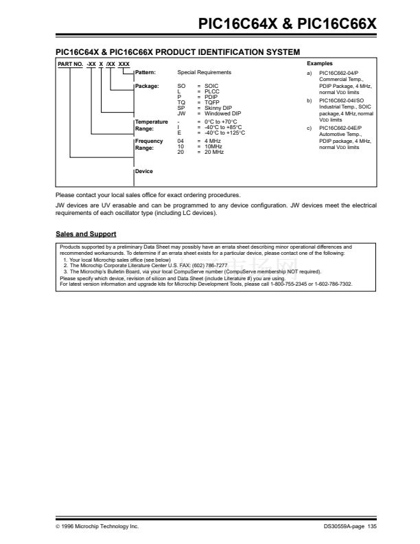
鈥?/div>
Literal and control
operations
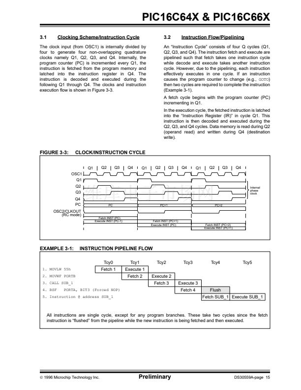
All instructions are executed within one single instruc-
tion cycle, unless a conditional test is true or the pro-
gram counter is changed as a result of an instruction.
In this case, the execution takes two instruction cycles
with the second cycle executed as a NOP. One instruc-
tion cycle consists of four oscillator periods. Thus, for
an oscillator frequency of 4 MHz, the normal instruction
execution time is 1
碌
s. If a conditional test is true or the
program counter is changed as a result of an instruc-
tion, the instruction execution time is 2
碌
s.
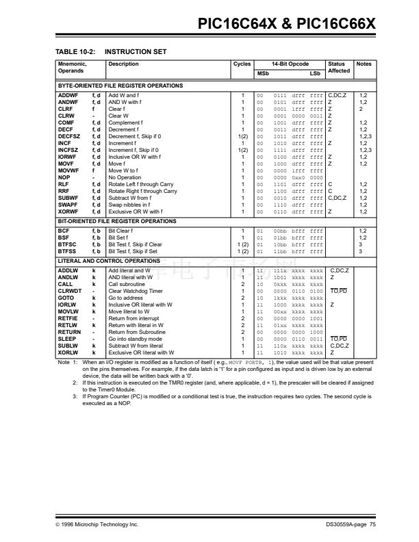
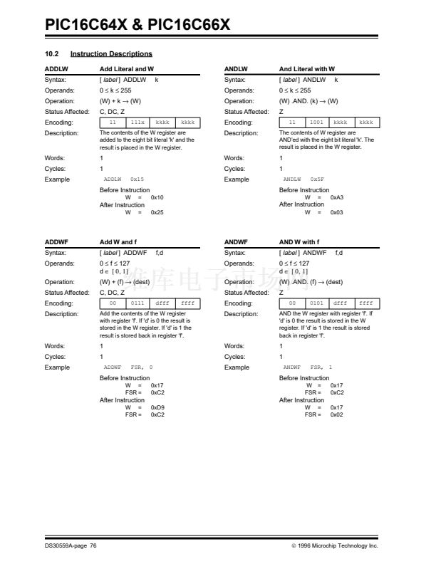
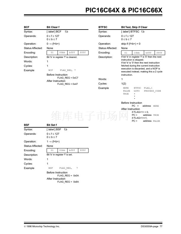
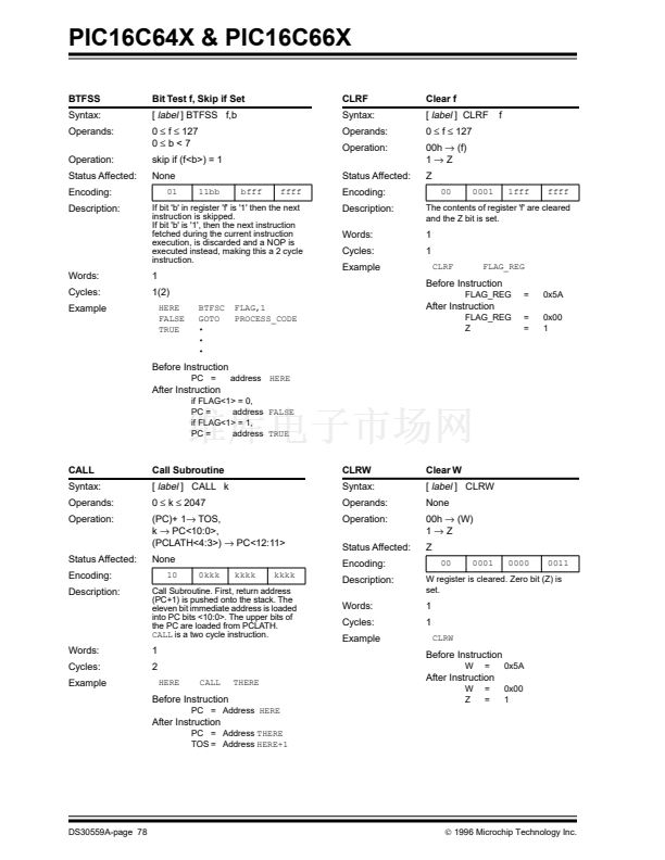
Table 10-2 lists the instructions recognized by the
MPASM assembler.
Figure 10-1 shows the three general formats that the
instructions can have.
Note:
To maintain upward compatibility with
future PIC16CXX products, do not use the
OPTION
and
TRIS
instructions.
All examples use the following format to represent a
hexadecimal number:
0xhh
where h signi铿乪s a hexadecimal digit.
TABLE 10-1:
Field
f
W
b
k
x
OPCODE FIELD
DESCRIPTIONS
Description
Register 铿乴e address (0x00 to 0x7F)
Working register (accumulator)
Bit address within an 8-bit 铿乴e register
Literal 铿乪ld, constant data or label
Don't care location (= 0 or 1)
The assembler will generate code with x = 0. It is the
recommended form of use for compatibility with all
Microchip software tools.
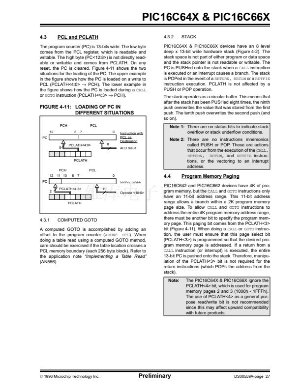
FIGURE 10-1: GENERAL FORMAT FOR
INSTRUCTIONS
Byte-oriented
铿乴e register operations
13
8 7 6
OPCODE
d
f (FILE #)
d = 0 for destination W
d = 1 for destination f
f = 7-bit 铿乴e register address
Bit-oriented
铿乴e register operations
13
10 9
7 6
OPCODE
b (BIT #)
f (FILE #)
b = 3-bit bit address
f = 7-bit 铿乴e register address
Literal and control
operations
General
13
8 7
OPCODE
k = 8-bit immediate value
CALL
and
GOTO
instructions only
13
11
OPCODE
10
k (literal)
0
0
0
Destination select; d = 0: store result in W,
d = 1: store result in 铿乴e register f.
Default is d = 1
label
Label name
d
TOS
PC
Top of Stack
Program Counter
PCLATH
Program Counter High Latch
GIE
Global Interrupt Enable bit
WDT
Watchdog Timer/Counter
TO
Time-out bit
PD
Power-down bit
dest
Destination either the W register or the speci铿乪d
register 铿乴e location
[ ] Options
( )
Contents
0
k (literal)
k = 11-bit immediate value
鈫?/div>
<>
鈭?/div>
Assigned to
Register bit 铿乪ld
In the set of
i
talics
User de铿乶ed term (font is courier)
The instruction set is highly orthogonal and is grouped
into three basic categories:
漏
1996 Microchip Technology Inc.
DS30559A-page 73
This document was created with FrameMaker 4 0 4


 1
1
 2
2
 3
3
 4
4
 5
5
 6
6
 7
7
 8
8
 9
9
 10
10
 11
11
 12
12
 13
13
 14
14
 15
15
 16
16
 17
17
 18
18
 19
19
 20
20
 21
21
 22
22
 23
23
 24
24
 25
25
 26
26
 27
27
 28
28
 29
29
 30
30
 31
31
 32
32
 33
33
 34
34
 35
35
 36
36
 37
37
 38
38
 39
39
 40
40
 41
41
 42
42
 43
43
 44
44
 45
45
 46
46
 47
47
 48
48
 49
49
 50
50
 51
51
 52
52
 53
53
 54
54
 55
55
 56
56
 57
57
 58
58
 59
59
 60
60
 61
61
 62
62
 63
63
 64
64
 65
65
 66
66
 67
67
 68
68
 69
69
 70
70
 71
71
 72
72
 73
73
 74
74
 75
75
 76
76
 77
77
 78
78
 79
79
 80
80
 81
81
 82
82
 83
83
 84
84
 85
85
 86
86
 87
87
 88
88
 89
89
 90
90
 91
91
 92
92
 93
93
 94
94
 95
95
 96
96
 97
97
 98
98
 99
99
 100
100
 101
101
 102
102
 103
103
 104
104
 105
105
 106
106
 107
107
 108
108
 109
109
 110
110
 111
111
 112
112
 113
113
 114
114
 115
115
 116
116
 117
117
 118
118
 119
119
 120
120
 121
121
 122
122
 123
123
 124
124
 125
125
 126
126
 127
127
 128
128
 129
129
 130
130
 131
131
 132
132
 133
133
 134
134
 135
135
 136
136
