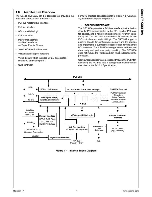
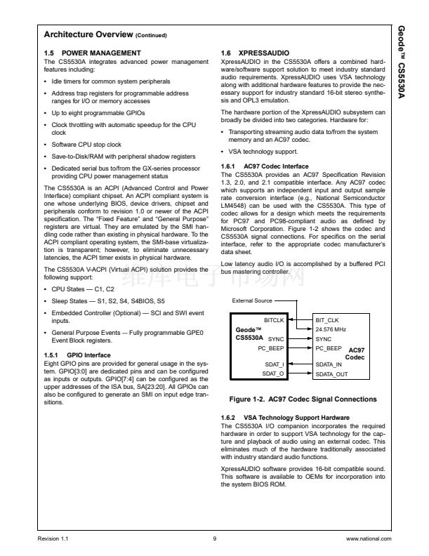
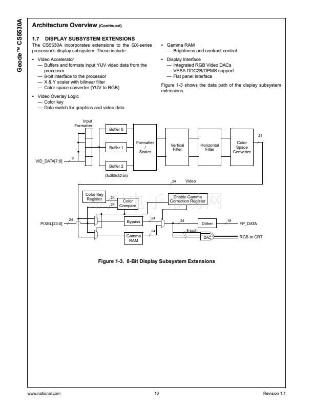
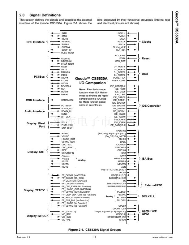
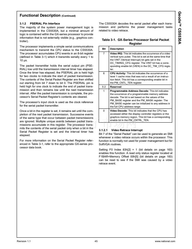
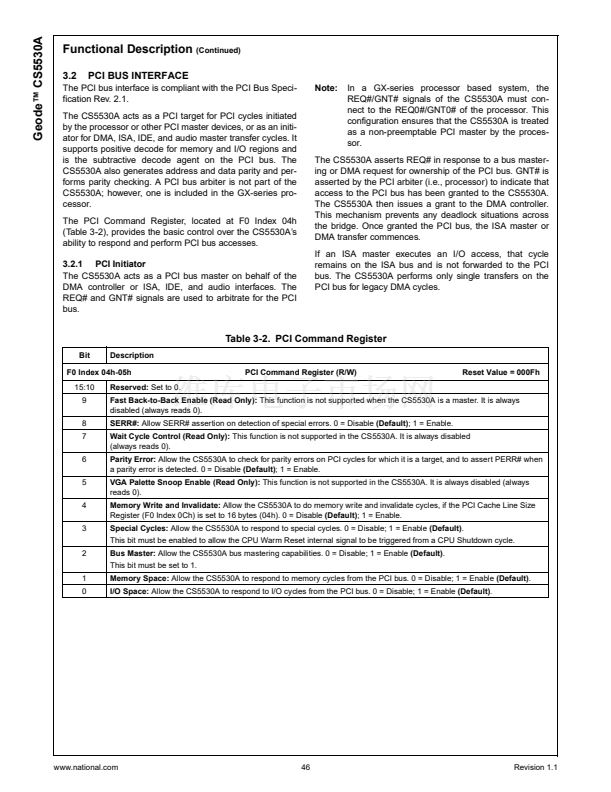
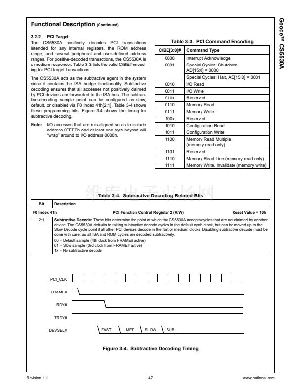
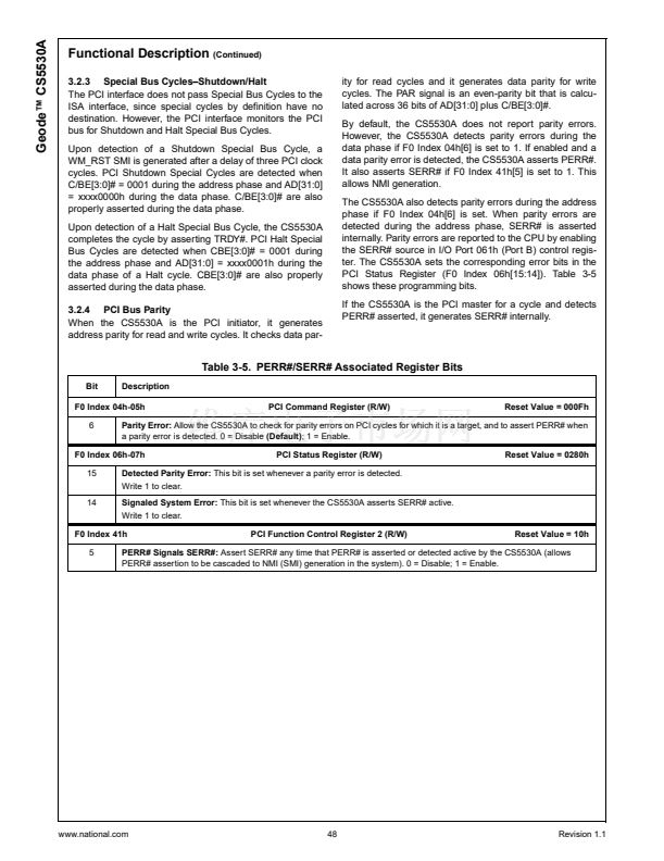
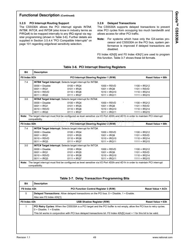
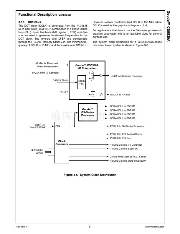
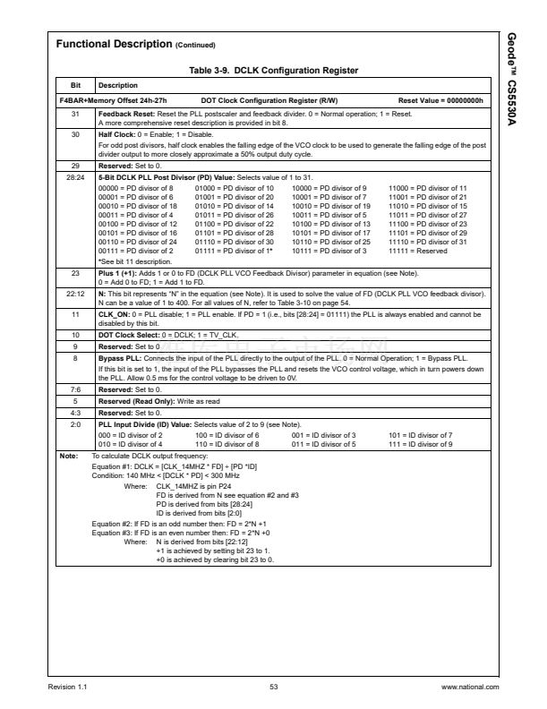
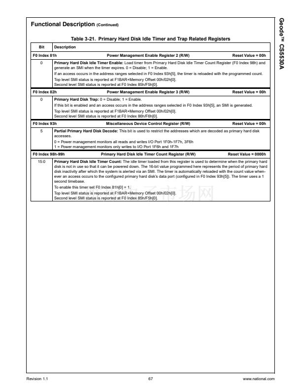
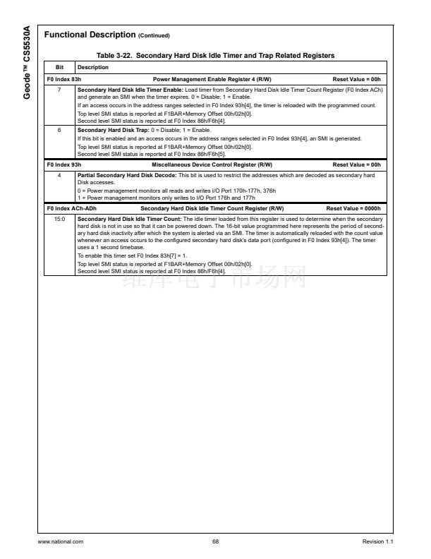
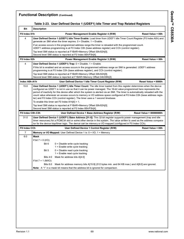
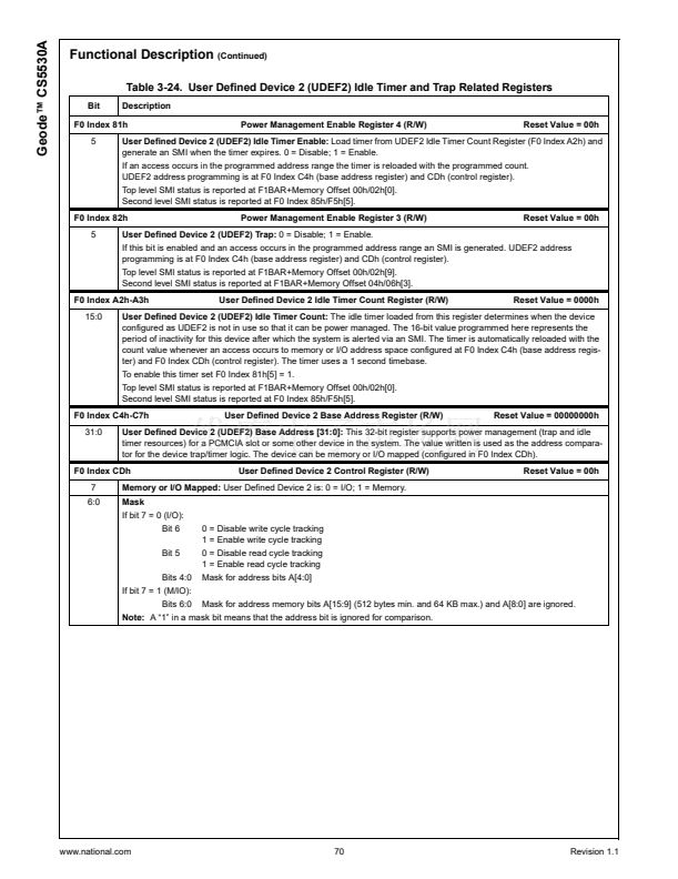
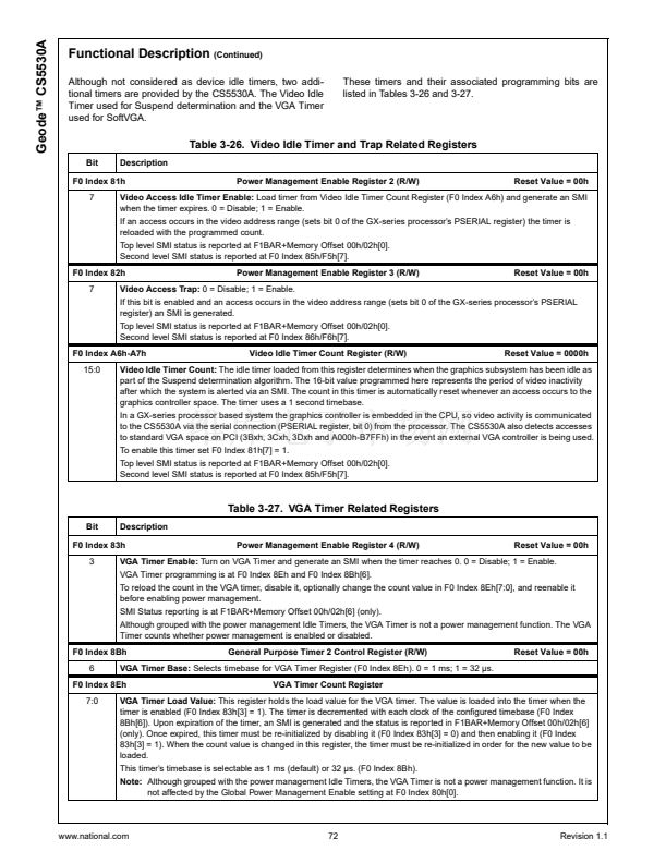
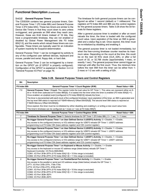
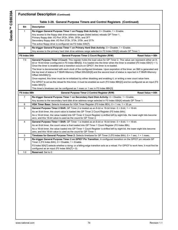
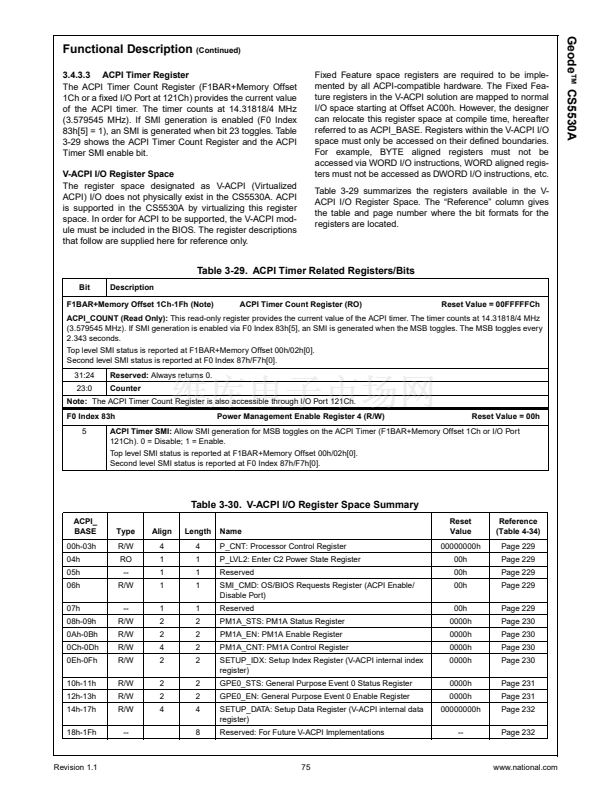
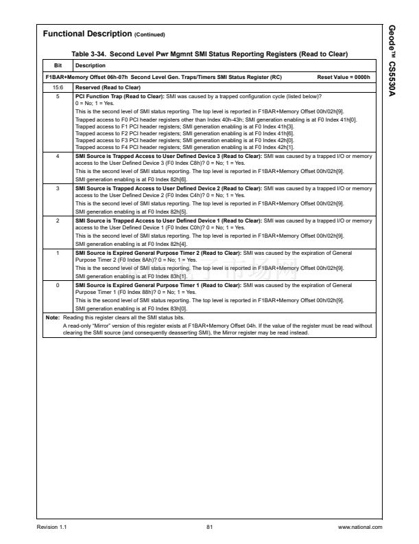
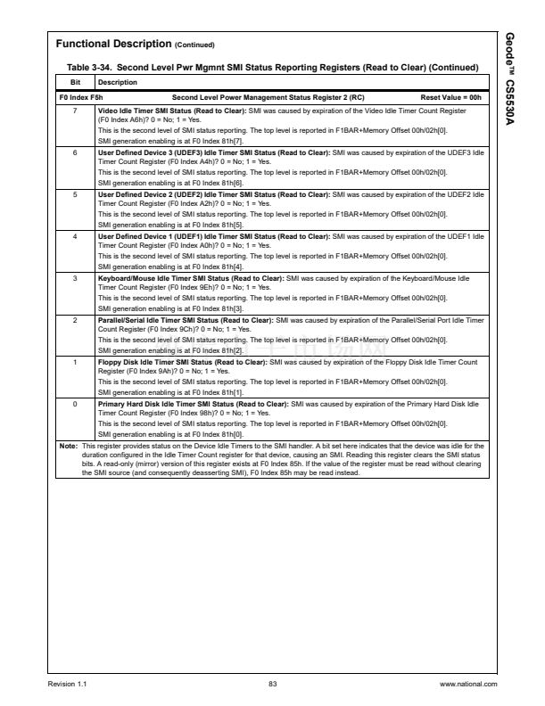
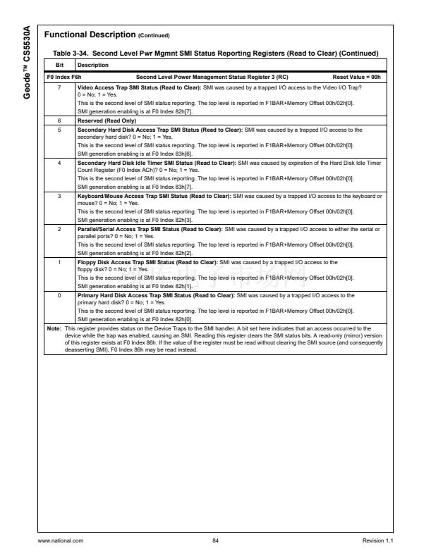
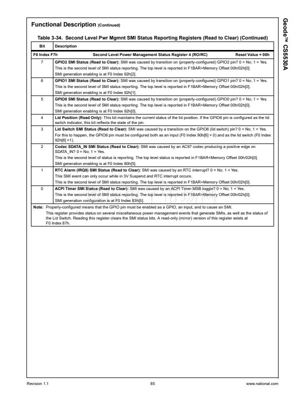
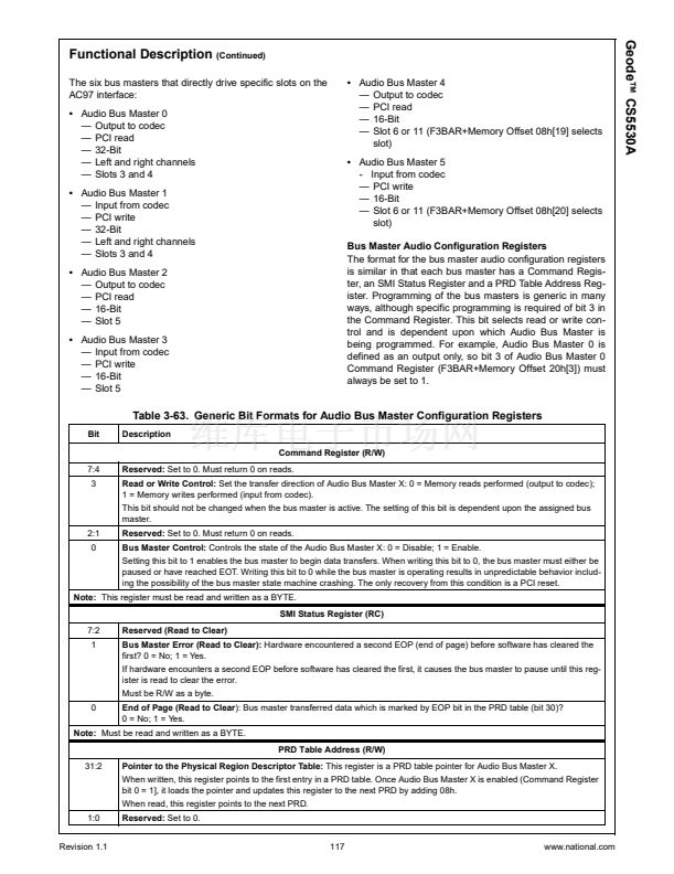
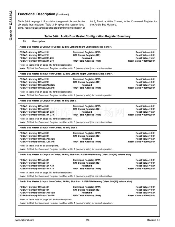
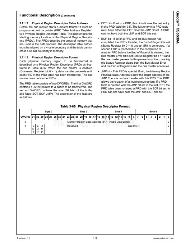
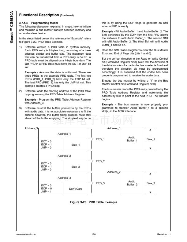
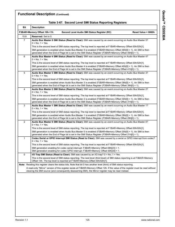
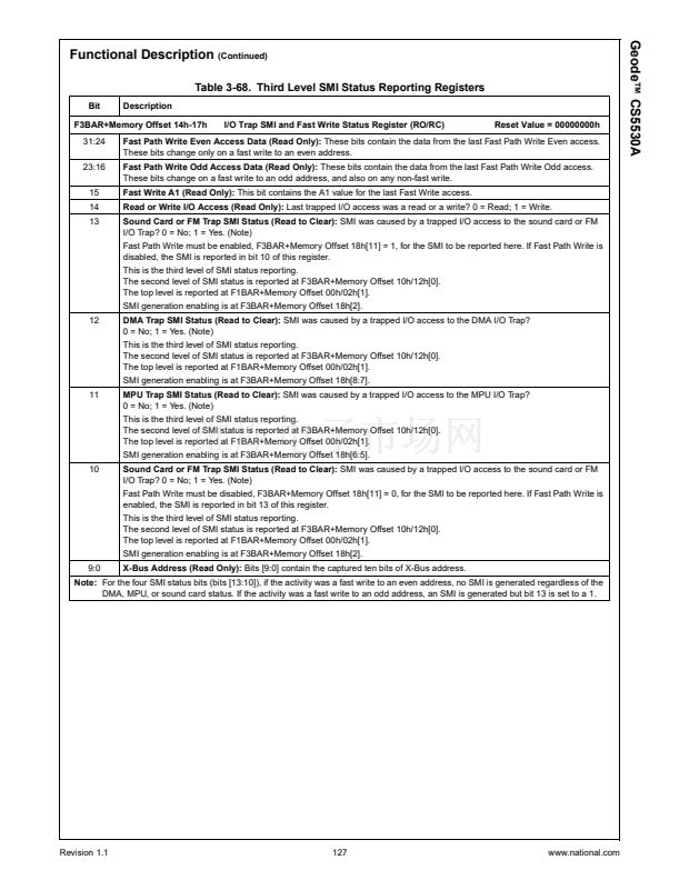
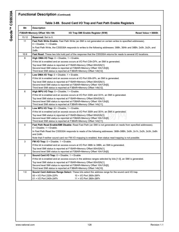
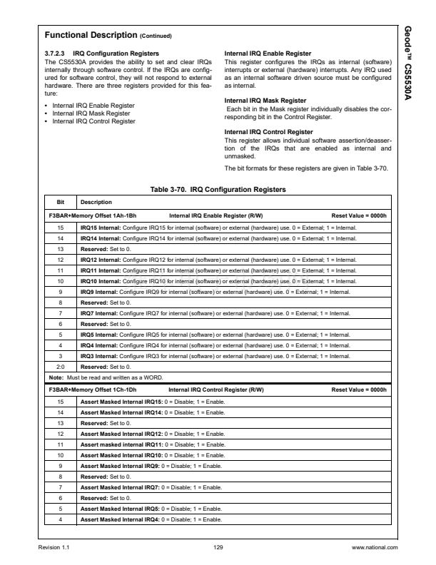
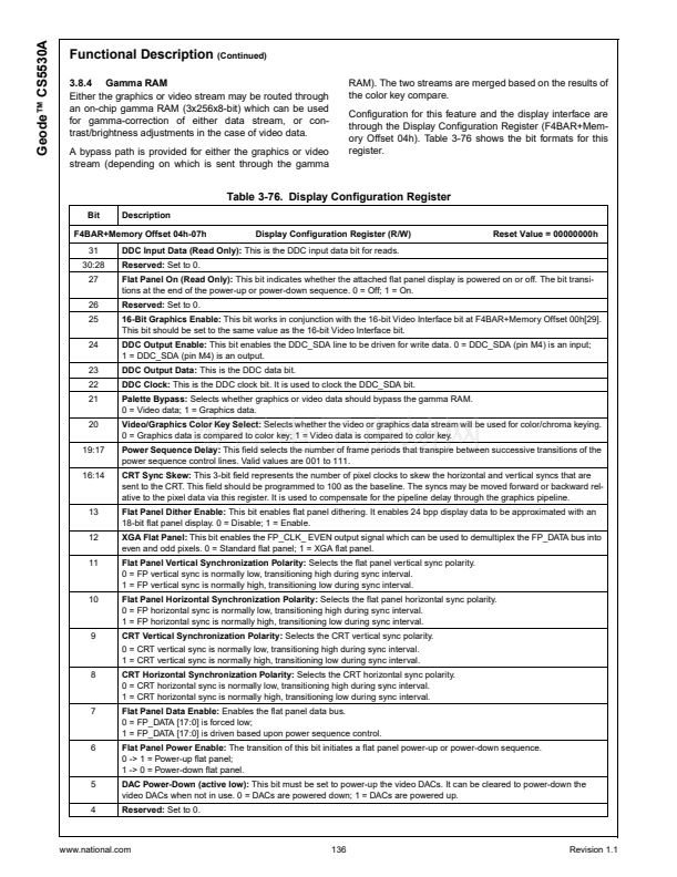
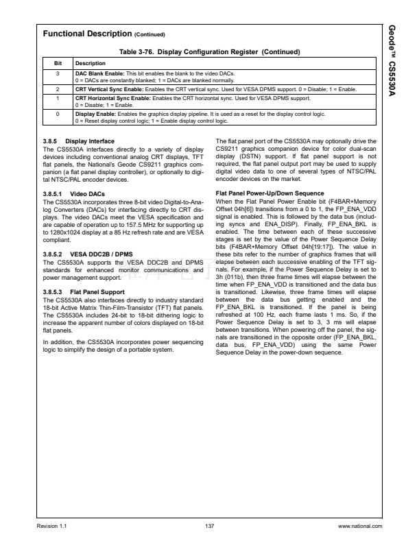
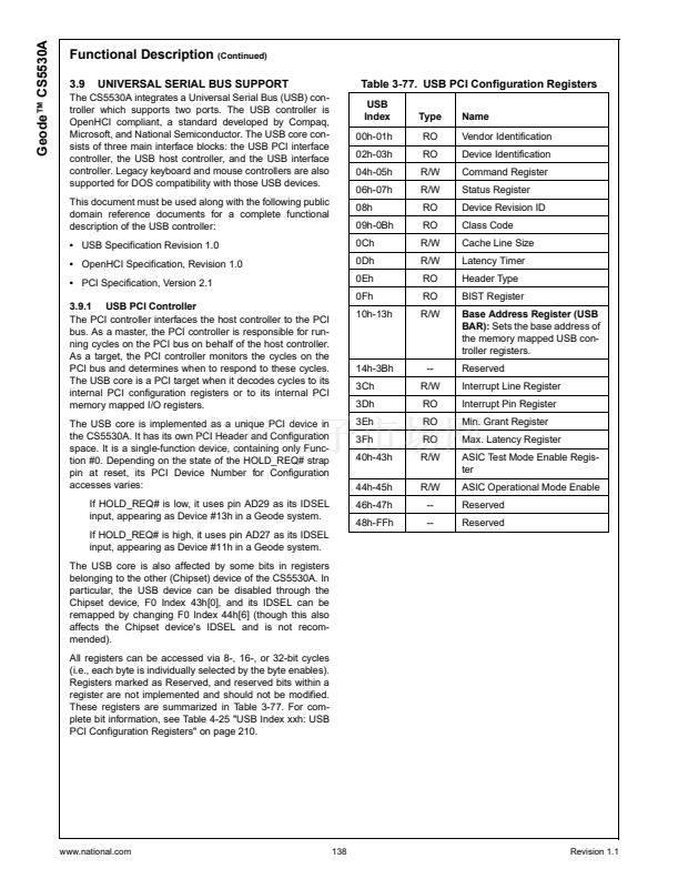
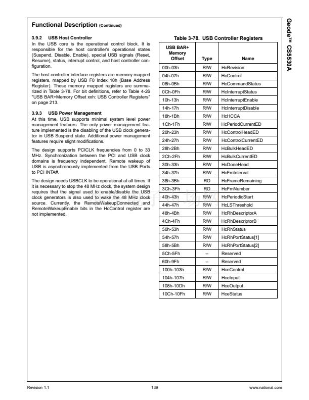
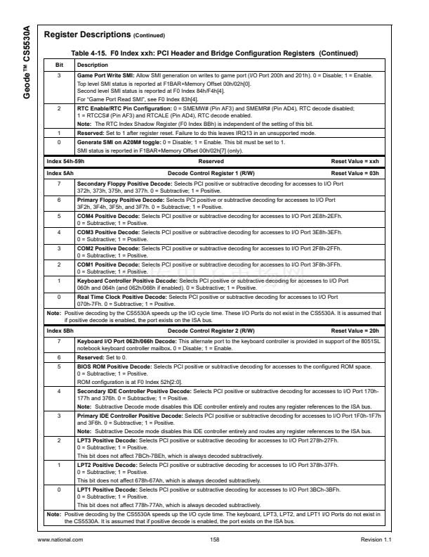
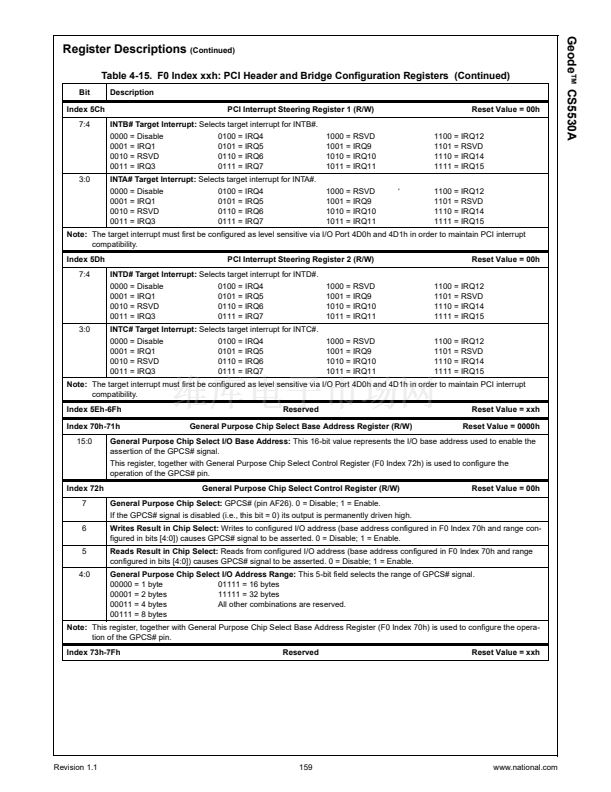
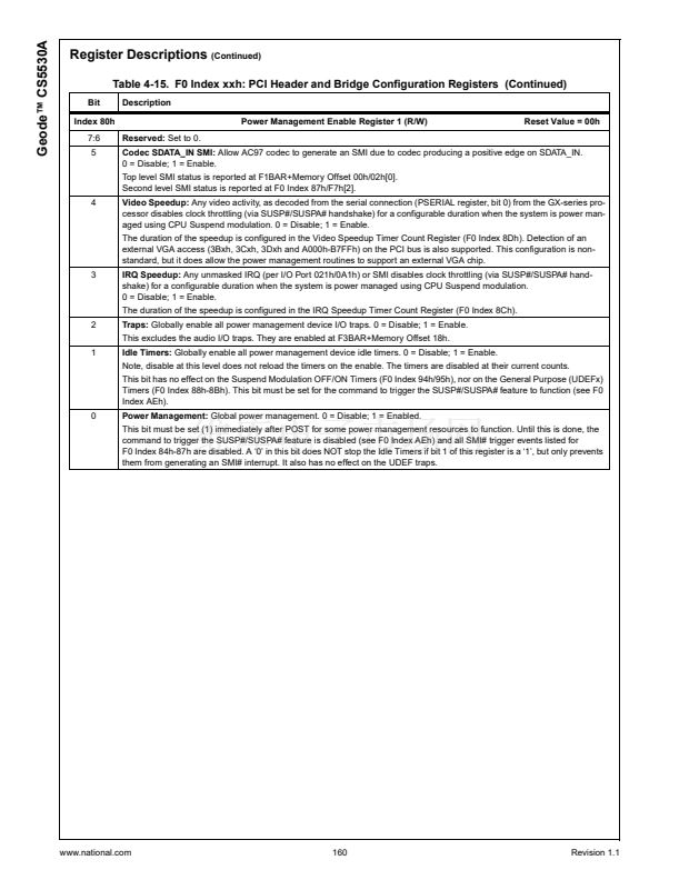
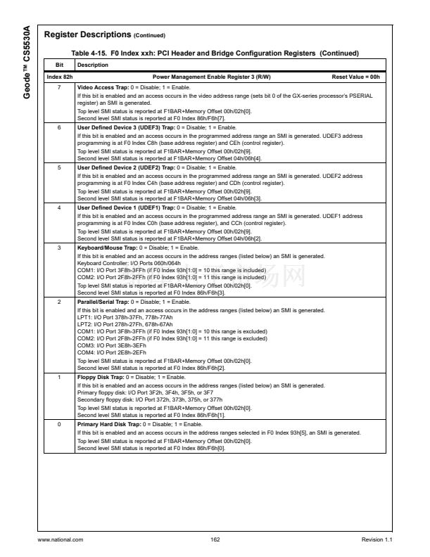
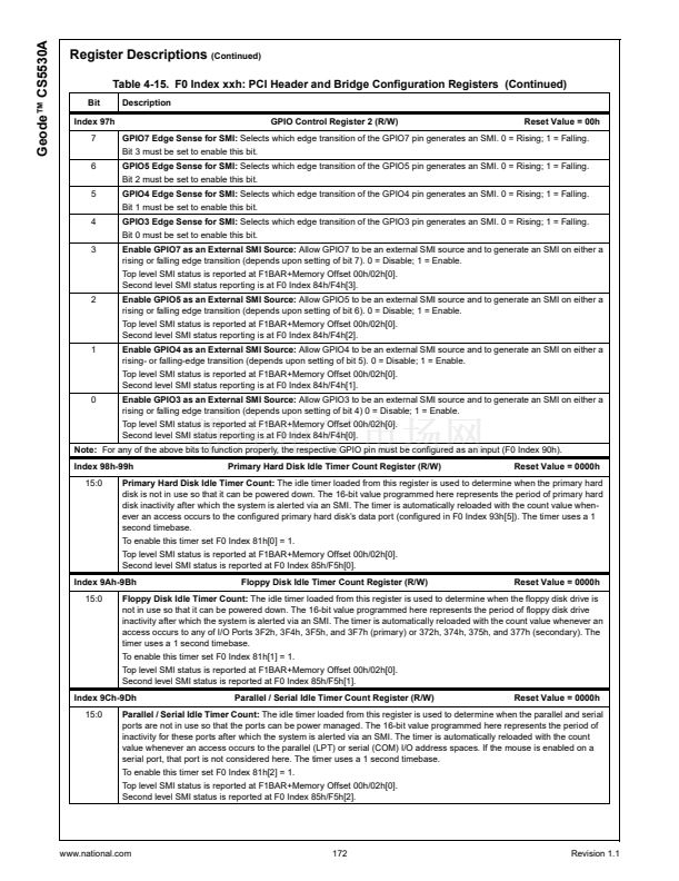
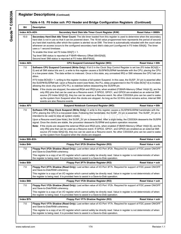
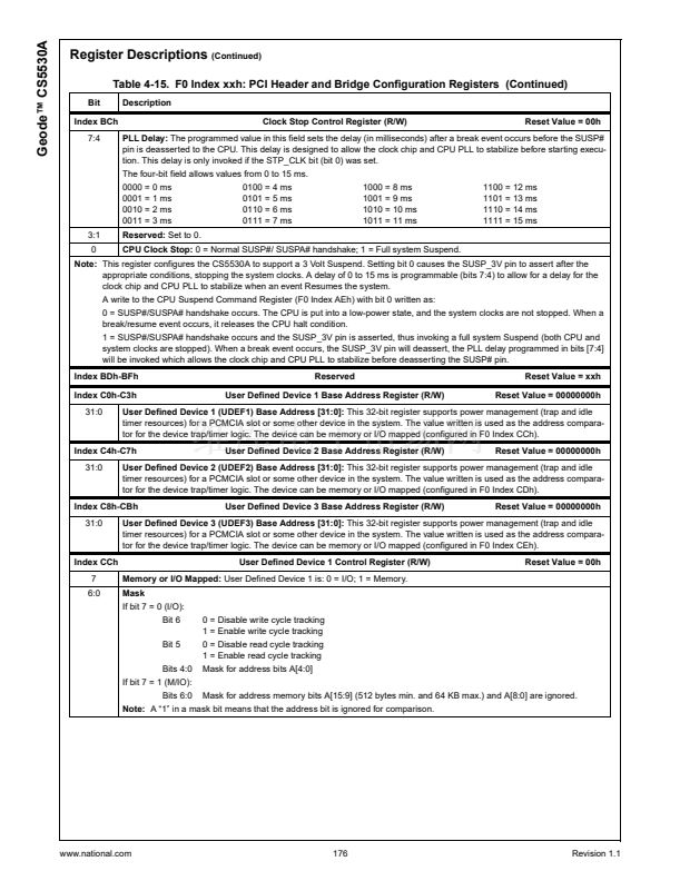
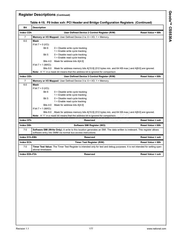
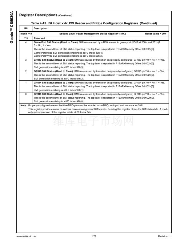
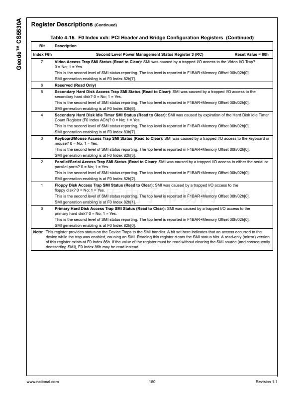
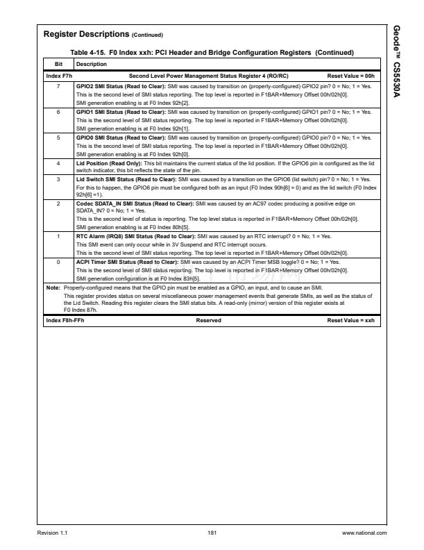
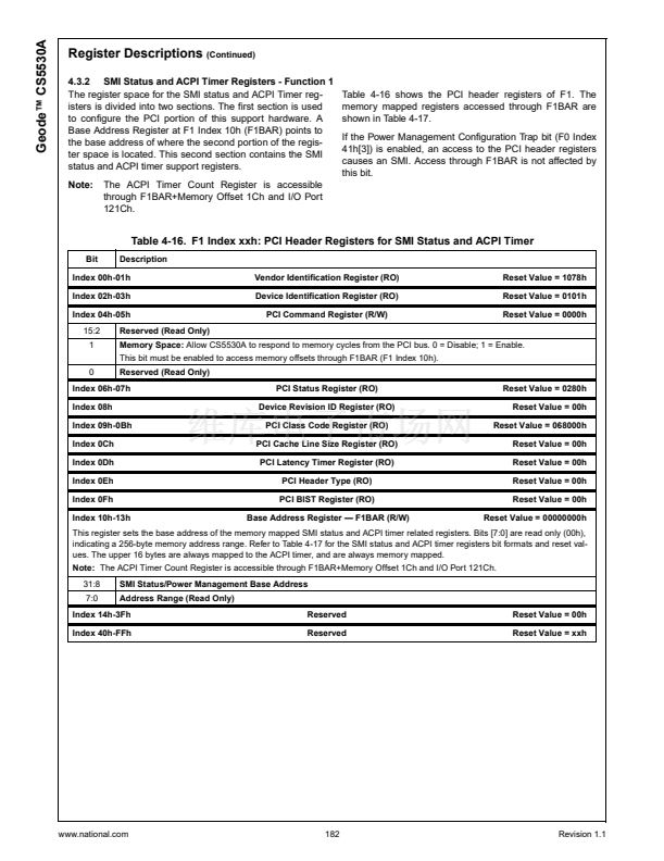
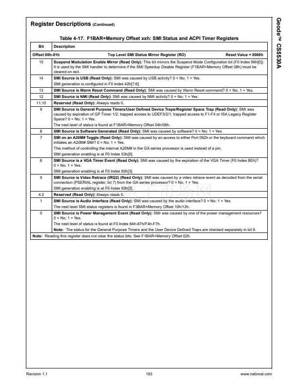
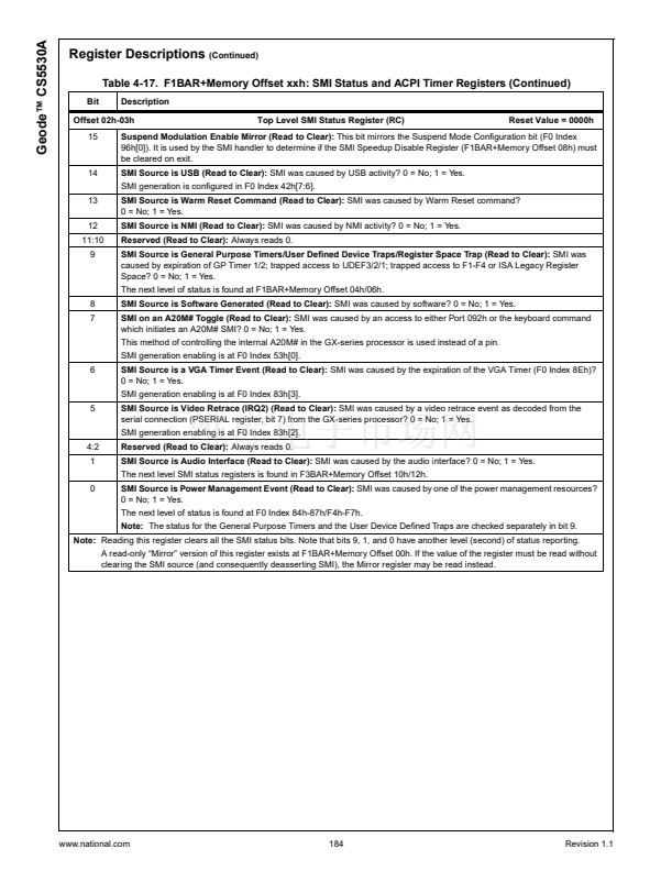
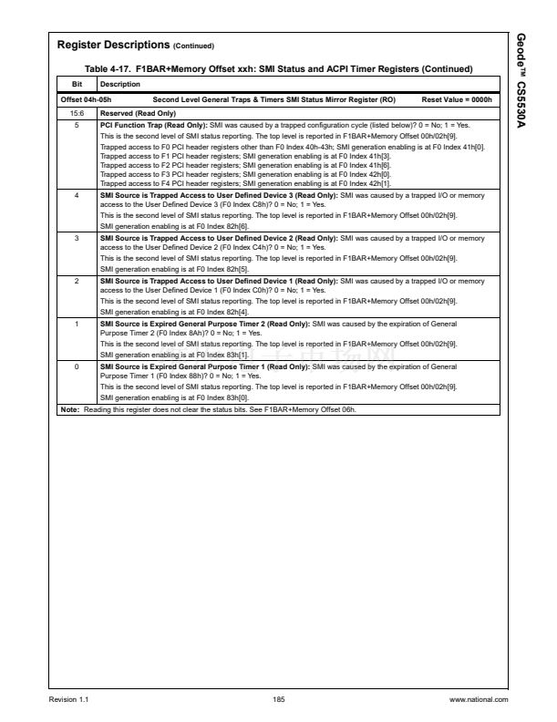
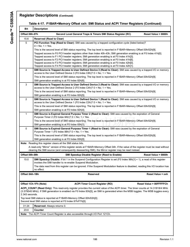
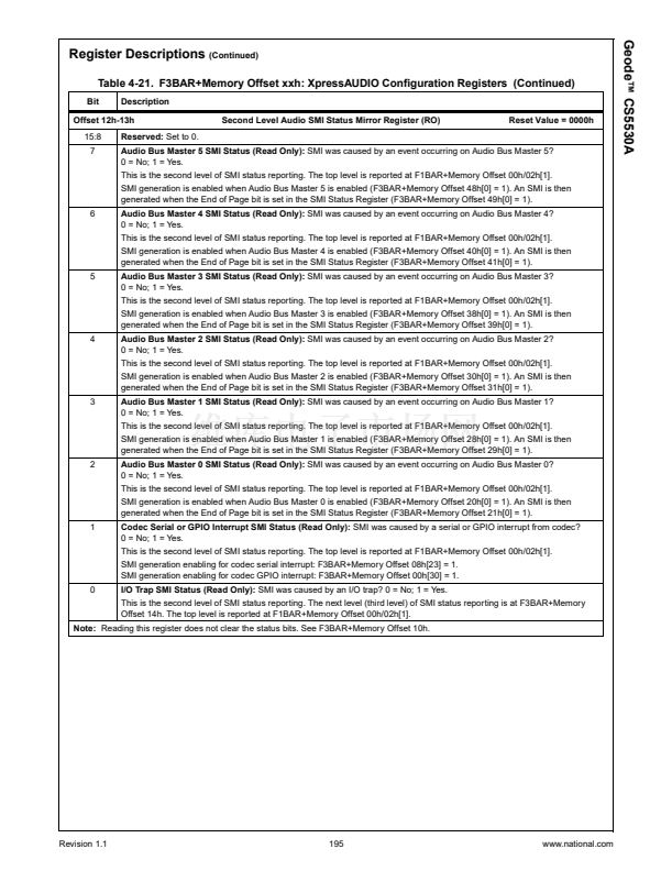
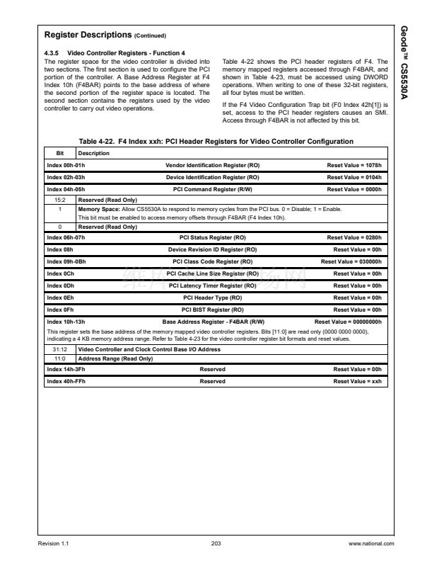
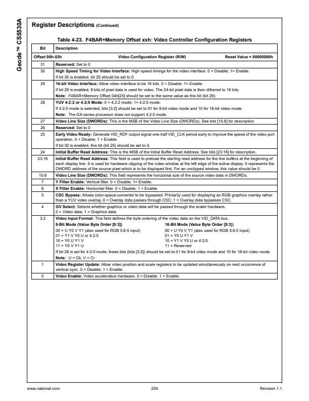
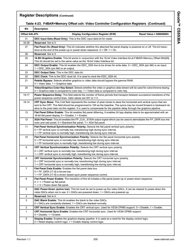
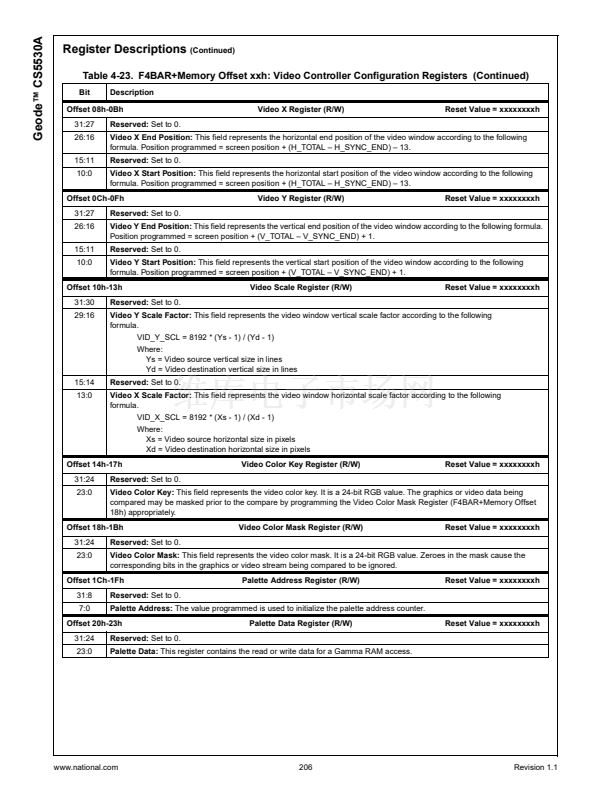
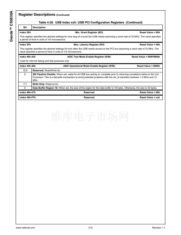
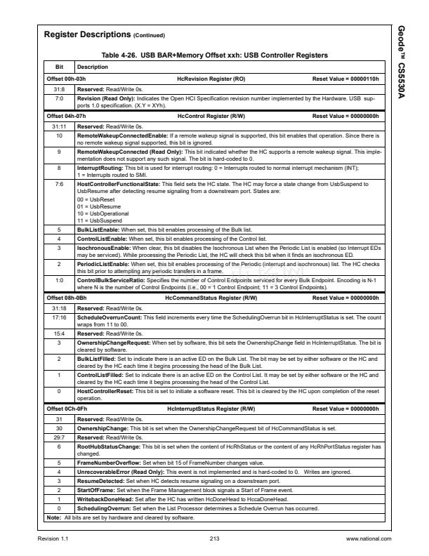
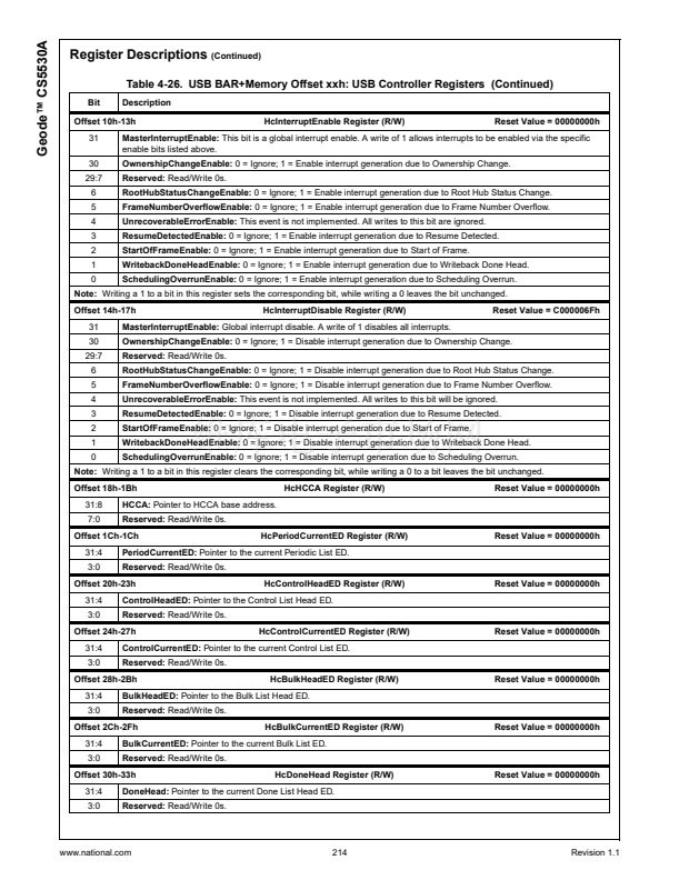
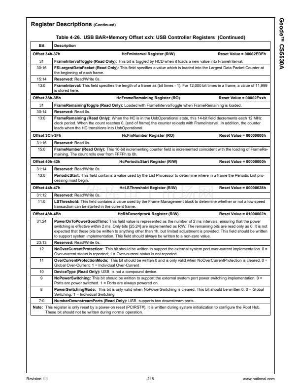
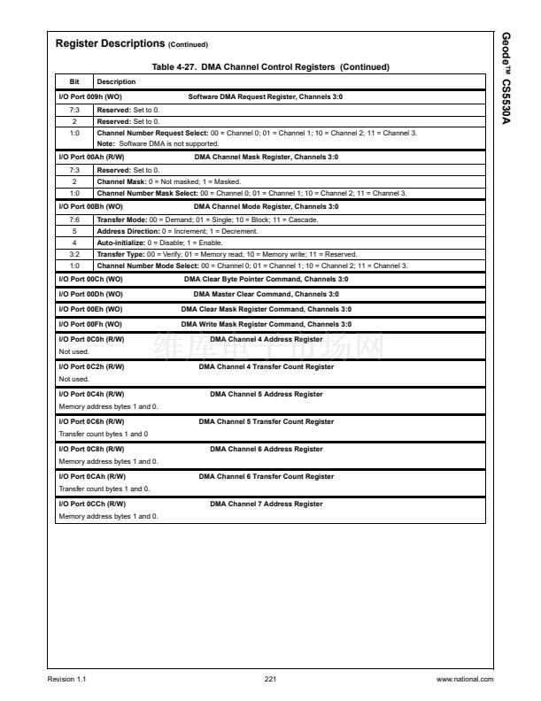
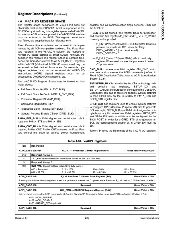
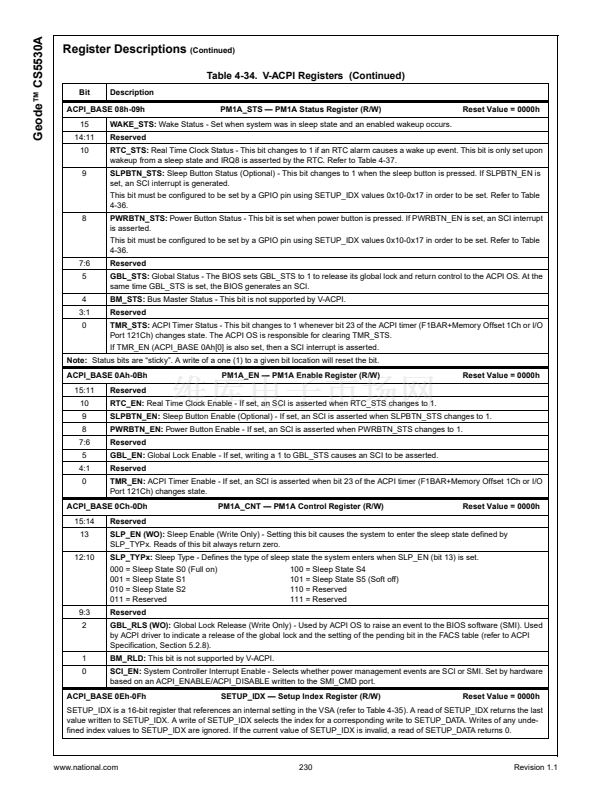
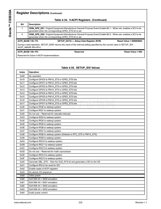
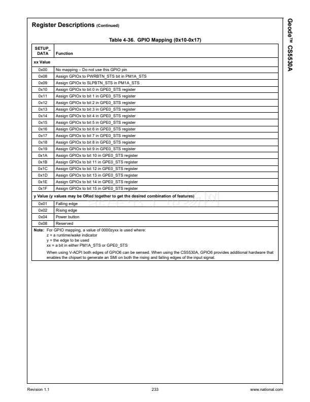
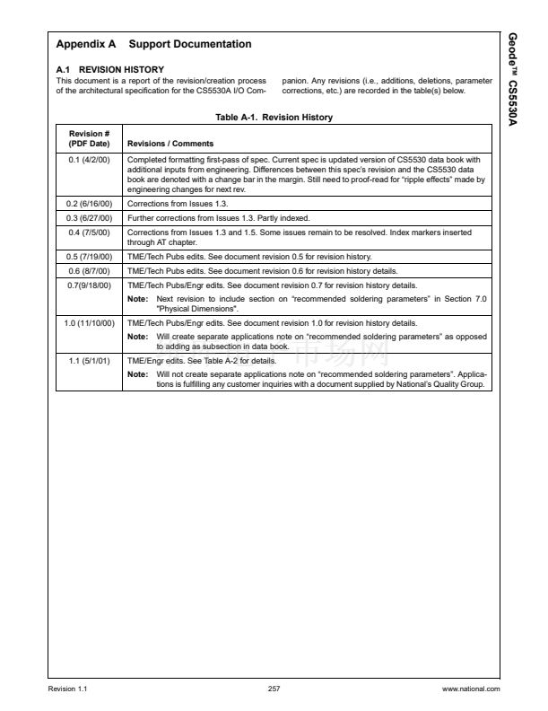
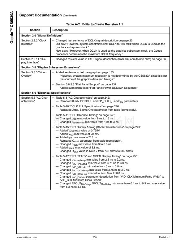
Geode鈩?CS5530A
Functional Description
(Continued)
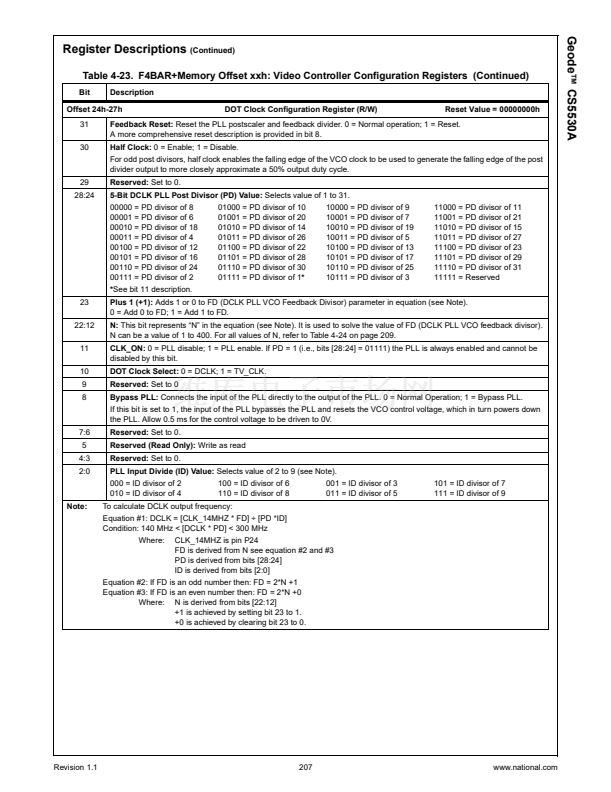
3.3.3.1 DCLK Programming
The PLL contains an input divider (ID), feedback divider
(FD) and a post divider (PD). The programming of the
dividers is through F4BAR+Memory Offset 24h (see Table
3-9 on page 53). The maximum output frequency is 300
MHz. The output frequency is given by equation #1:
Equation #1:
DCLK = [CLK_14MHZ * FD] 梅 [PD *ID]
Condition:
140 MHz < [DCLK * PD] < 300 MHz
Where:
CLK_14MHZ is pin P24
FD is derived from N see equation #2 and #3:
PD is derived from bits [28:24]
ID is derived from bits [2:0]
Equation #2:
If FD is an odd number then: FD = 2*N +1
Equation #3:
If FD is an even number then: FD = 2*N +0
Where:
N is derived from bits [22:12]
+1 is achieved by setting bit 23 to 1.
+0 is achieved by clearing bit 23 to 0.
Example
Define Target Frequency:
Target frequency = 135 MHz
Satisfy the 鈥淐ondition鈥?
(140 MHz < [DCLK * PD] < 300 MHz)
140 MHz < [135 MHz * 2] < 300 MHz
Therefore PD = 2
Solve Equation #1:
DCLK = [CLK_14MHZ * FD] 梅 [PD *ID]
135 = [14.31818 * FD] 梅 [2 * ID]
135 = [7.159 * FD] 梅 ID
18.86 = FD 梅 ID
Guess: ID = 7, Solve for FD
FD = 132.02
Solve Equation #2 or #3:
FD = 2*N +1 for odd FD
FD = 2*N +0 for even FD
FD is 132, therefore even
132 = 2*N +0
N = 66
Summarize:
PD = 2: Bits [28:24] = 00111
ID = 7: Bits [2:0] = 101
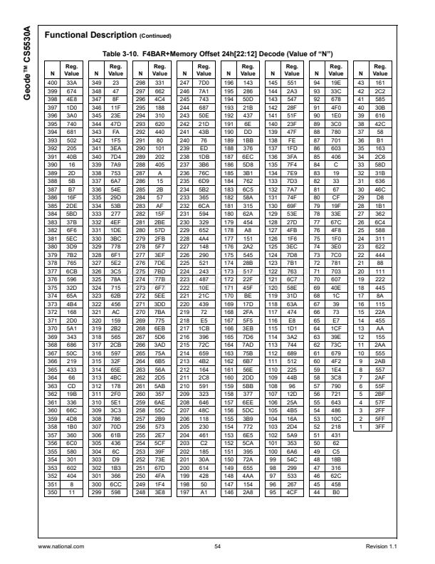
N = 66: Bits [22:12] = 073h (found in Table 3-10), clear
bit 23
Result:
DCLK = 135
The BIOS has been provided with a complete table of divi-
sor values for supported graphics clock frequencies. Many
combinations of divider values and VCO frequencies are
possible to achieve a certain output clock frequency. These
BIOS values may be adjusted from time to time to meet
system frequency accuracy and jitter requirements. For
applications that do not use the GX-series processor鈥檚
graphics subsystem, this is an available clock for general
purpose use.
The transition from one DCLK frequency to another is not
guaranteed to be smooth or bounded; therefore, new
divider coefficients should only be programmed while the
PLL is off line in a situation where the transition character-
istics of the clock are 鈥渄on't care鈥? The steps below
describe (in order) how to change the DCLK frequency.
1)
2)
3)
4)
5)
Program the new clock frequency.
Program Feedback Reset (bit 31) high and Bypass
PLL (bit 8) high.
Wait at least 500 碌s for PLL to settle.
Program Feedback Reset (bit 31) low.
Program Bypass PLL (bit 8) low.
www.national.com
52
Revision 1.1


 1
1
 2
2
 3
3
 4
4
 5
5
 6
6
 7
7
 8
8
 9
9
 10
10
 11
11
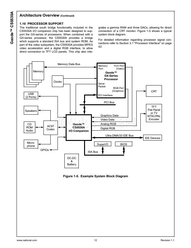 12
12
 13
13
 14
14
 15
15
 16
16
 17
17
 18
18
 19
19
 20
20
 21
21
 22
22
 23
23
 24
24
 25
25
 26
26
 27
27
 28
28
 29
29
 30
30
 31
31
 32
32
 33
33
 34
34
 35
35
 36
36
 37
37
 38
38
 39
39
 40
40
 41
41
 42
42
 43
43
 44
44
 45
45
 46
46
 47
47
 48
48
 49
49
 50
50
 51
51
 52
52
 53
53
 54
54
 55
55
 56
56
 57
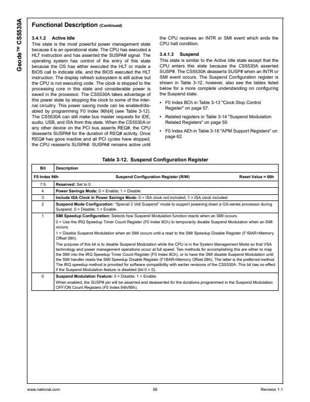
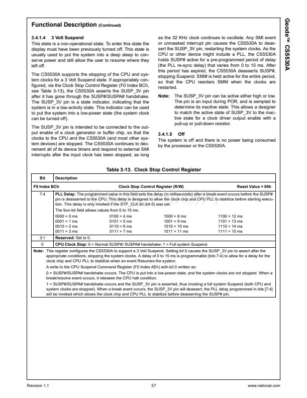
57
 58
58
 59
59
 60
60
 61
61
 62
62
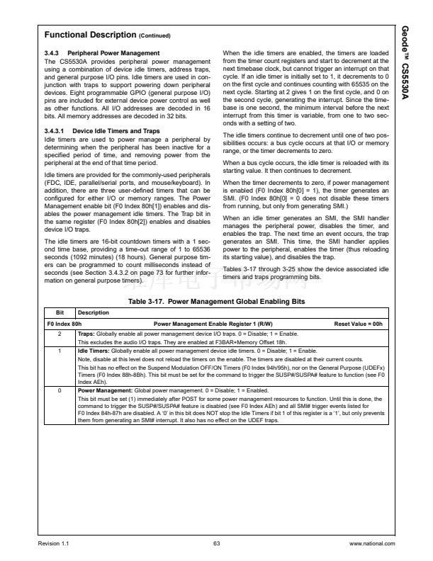 63
63
 64
64
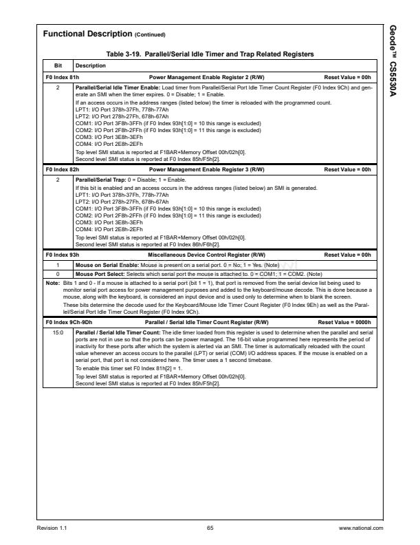 65
65
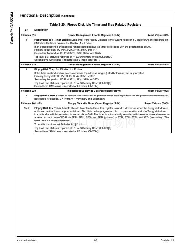 66
66
 67
67
 68
68
 69
69
 70
70
 71
71
 72
72
 73
73
 74
74
 75
75
 76
76
 77
77
 78
78
 79
79
 80
80
 81
81
 82
82
 83
83
 84
84
 85
85
 86
86
 87
87
 88
88
 89
89
 90
90
 91
91
 92
92
 93
93
 94
94
 95
95
 96
96
 97
97
 98
98
 99
99
 100
100
 101
101
 102
102
 103
103
 104
104
 105
105
 106
106
 107
107
 108
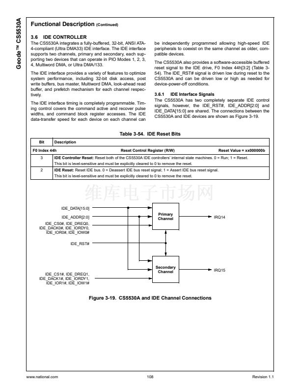
108
 109
109
 110
110
 111
111
 112
112
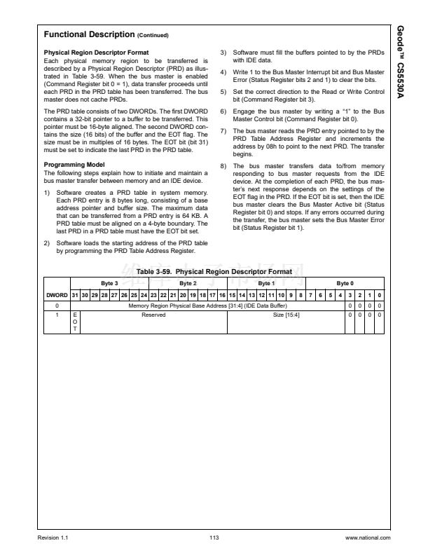 113
113
 114
114
 115
115
 116
116
 117
117
 118
118
 119
119
 120
120
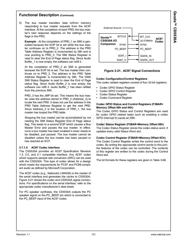 121
121
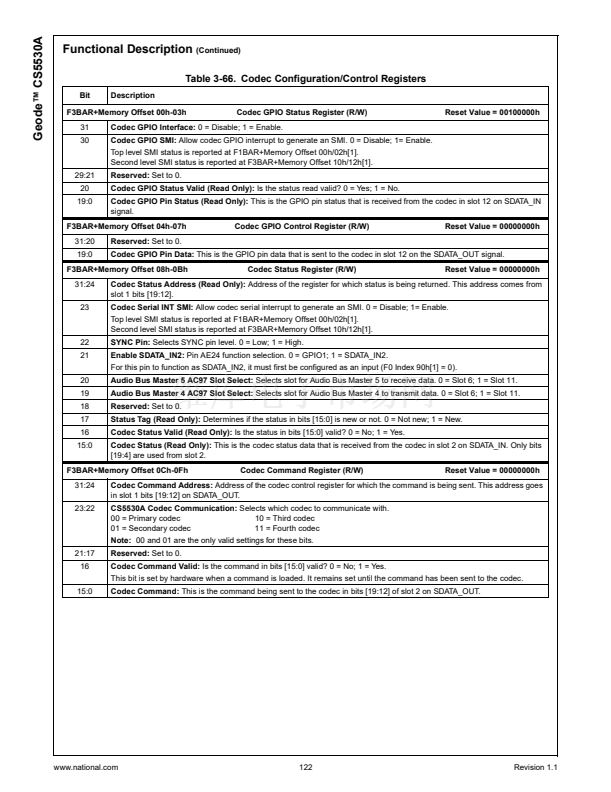 122
122
 123
123
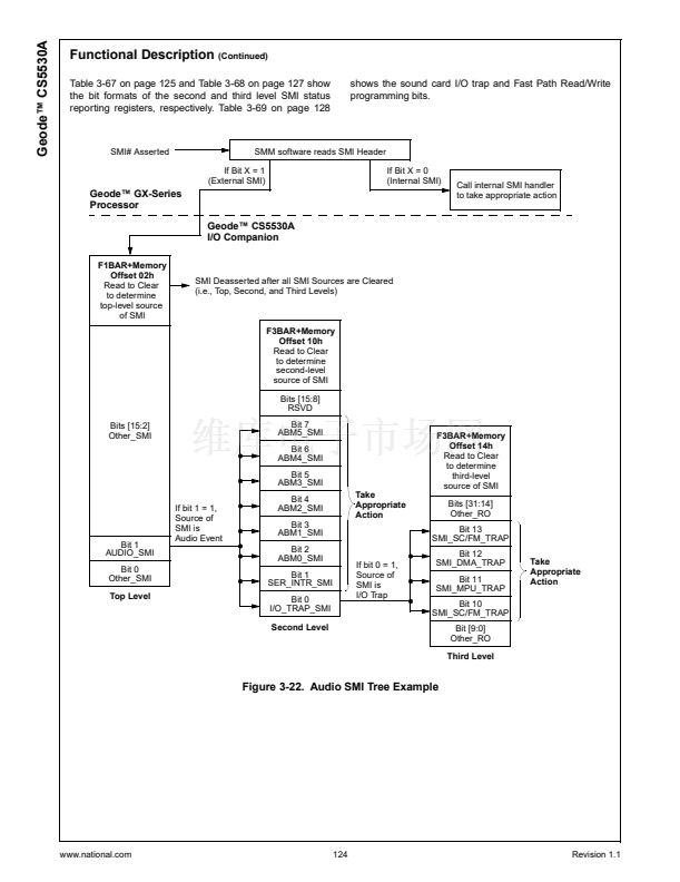 124
124
 125
125
 126
126
 127
127
 128
128
 129
129
 130
130
 131
131
 132
132
 133
133
 134
134
 135
135
 136
136
 137
137
 138
138
 139
139
 140
140
 141
141
 142
142
 143
143
 144
144
 145
145
 146
146
 147
147
 148
148
 149
149
 150
150
 151
151
 152
152
 153
153
 154
154
 155
155
 156
156
 157
157
 158
158
 159
159
 160
160
 161
161
 162
162
 163
163
 164
164
 165
165
 166
166
 167
167
 168
168
 169
169
 170
170
 171
171
 172
172
 173
173
 174
174
 175
175
 176
176
 177
177
 178
178
 179
179
 180
180
 181
181
 182
182
 183
183
 184
184
 185
185
 186
186
 187
187
 188
188
 189
189
 190
190
 191
191
 192
192
 193
193
 194
194
 195
195
 196
196
 197
197
 198
198
 199
199
 200
200
 201
201
 202
202
 203
203
 204
204
 205
205
 206
206
 207
207
 208
208
 209
209
 210
210
 211
211
 212
212
 213
213
 214
214
 215
215
 216
216
 217
217
 218
218
 219
219
 220
220
 221
221
 222
222
 223
223
 224
224
 225
225
 226
226
 227
227
 228
228
 229
229
 230
230
 231
231
 232
232
 233
233
 234
234
 235
235
 236
236
 237
237
 238
238
 239
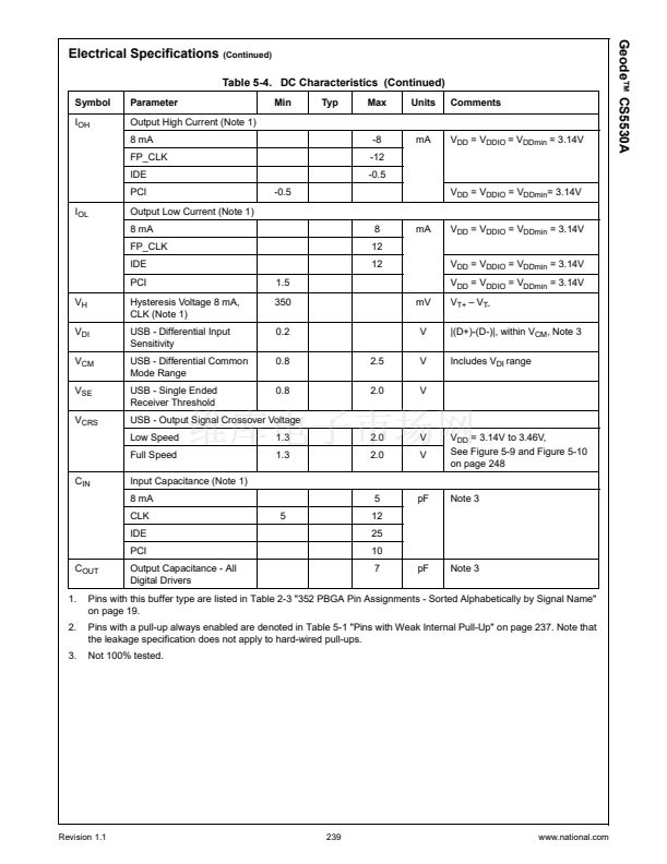
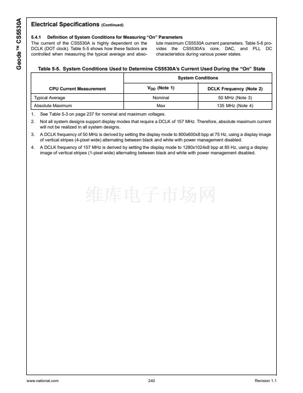
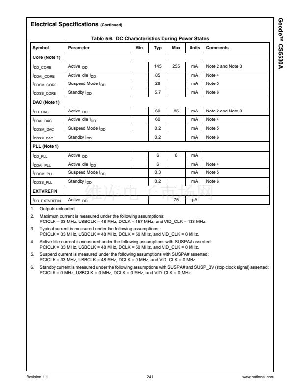
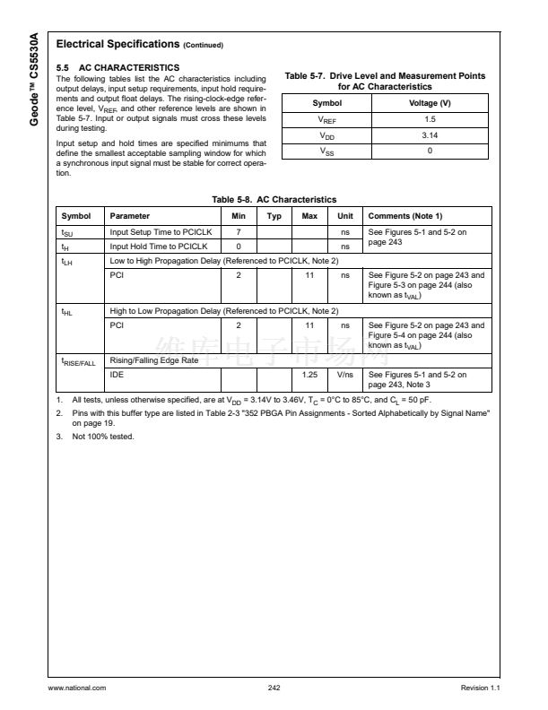
239
 240
240
 241
241
 242
242
 243
243
 244
244
 245
245
 246
246
 247
247
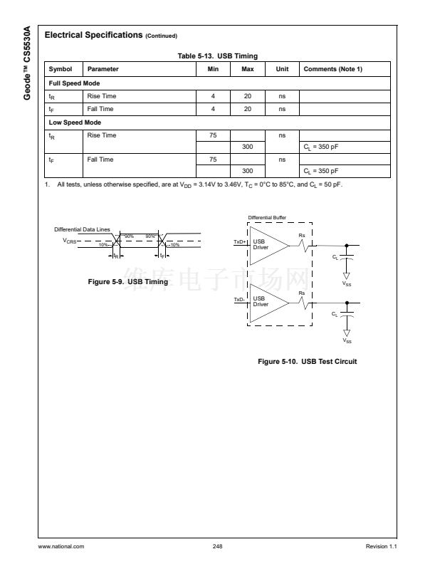 248
248
 249
249
 250
250
 251
251
 252
252
 253
253
 254
254
 255
255
 256
256
 257
257
 258
258
 259
259
