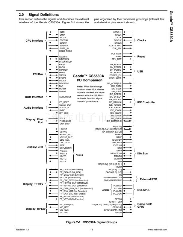
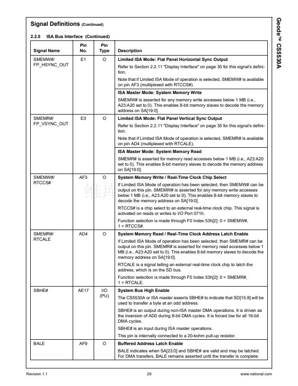
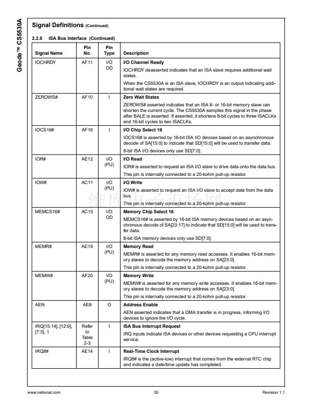
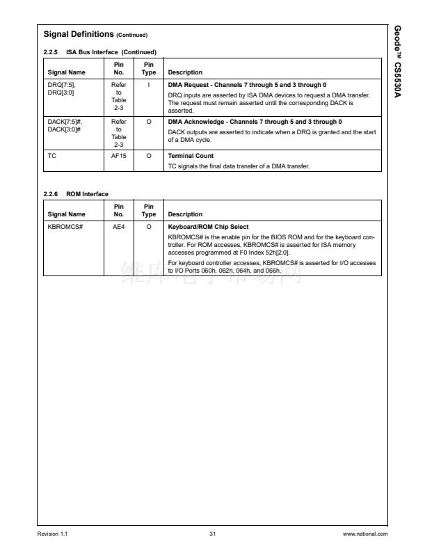
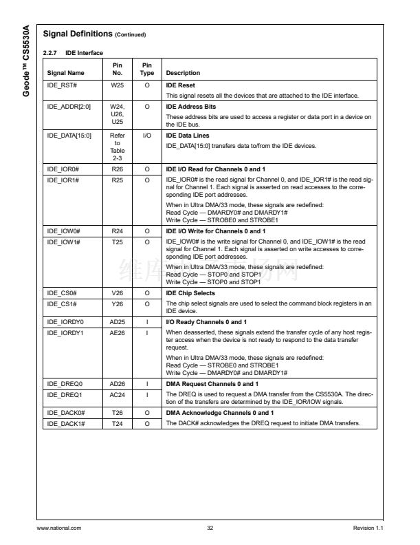
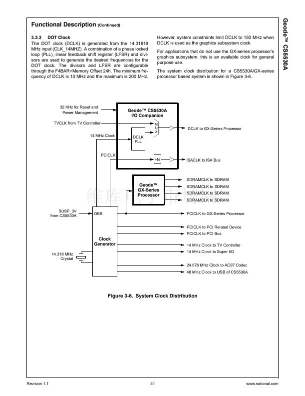
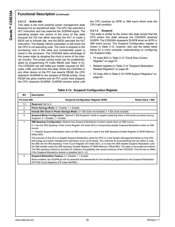
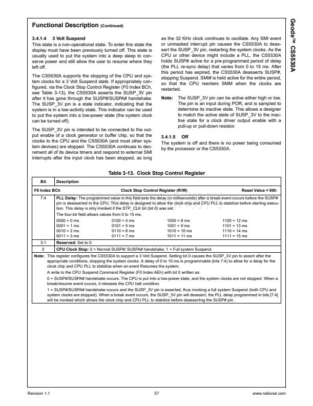
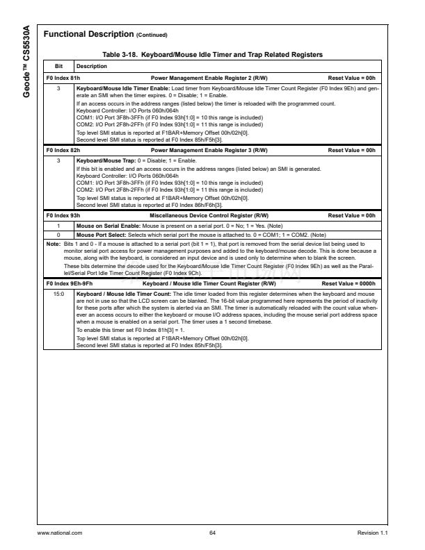
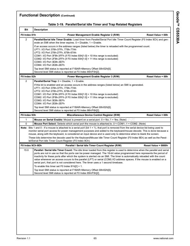
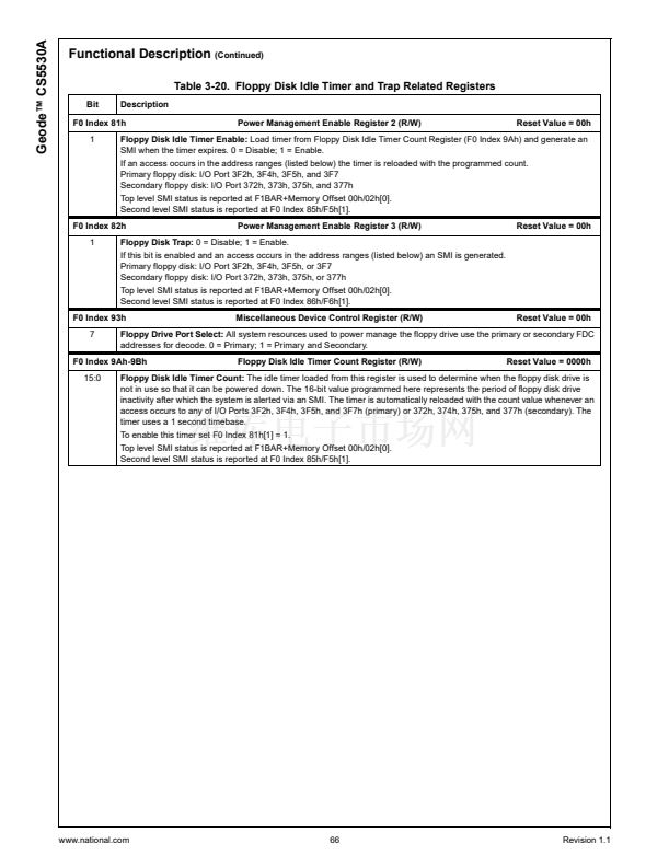
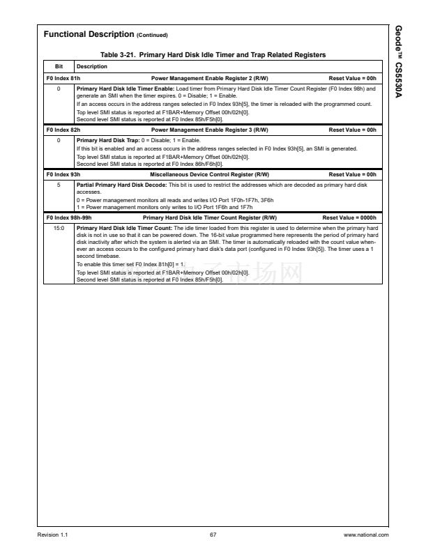
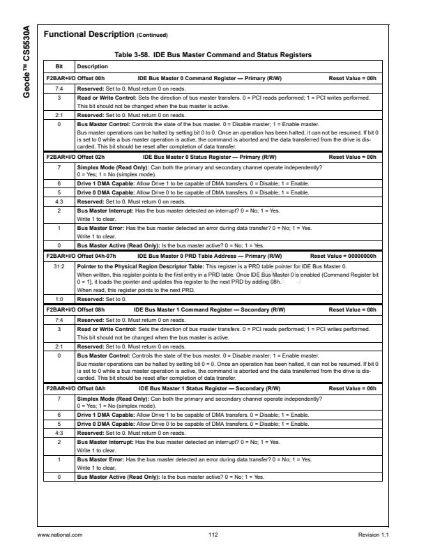
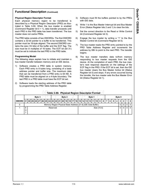
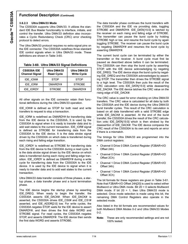
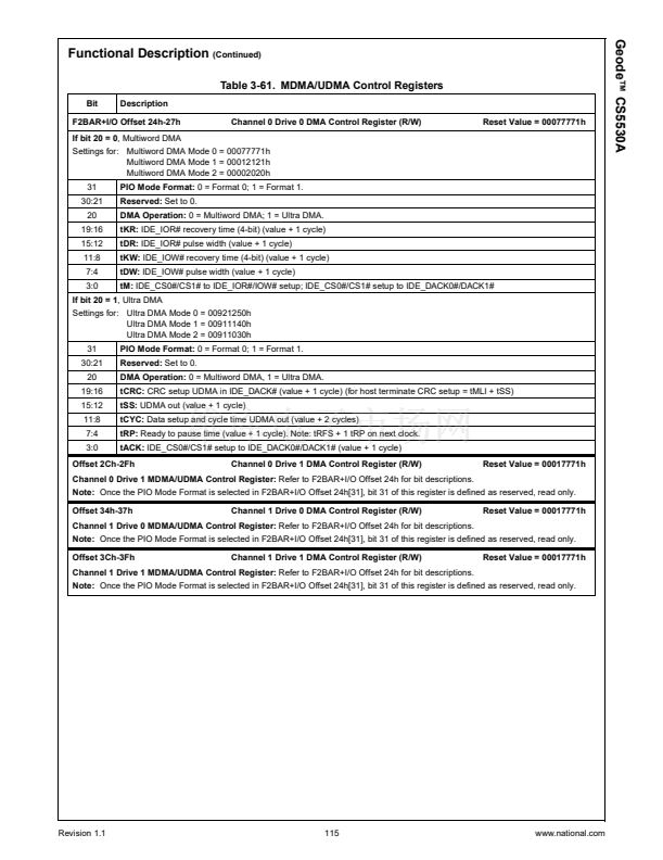
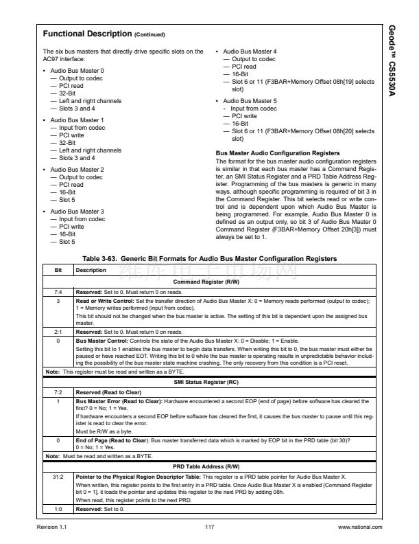
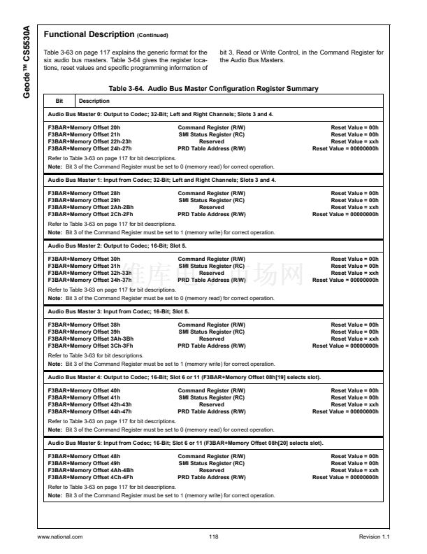
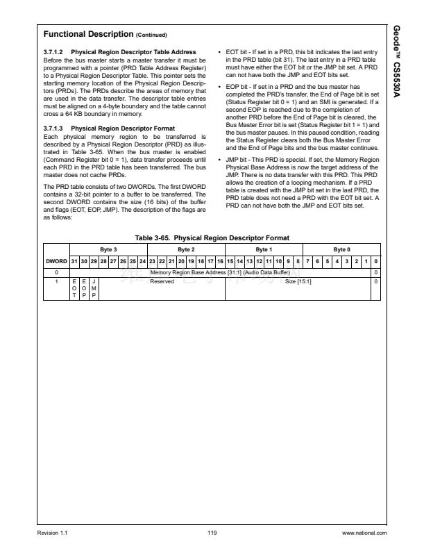
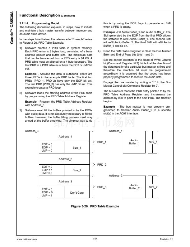
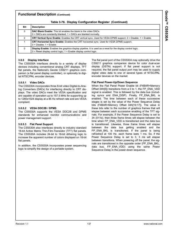
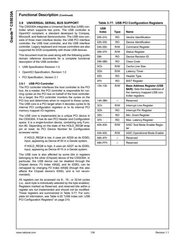
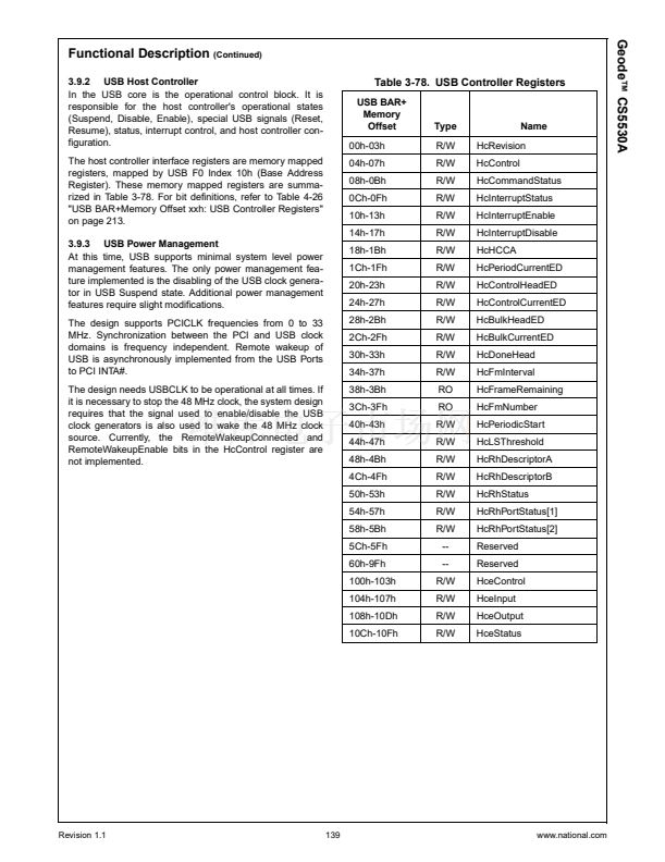
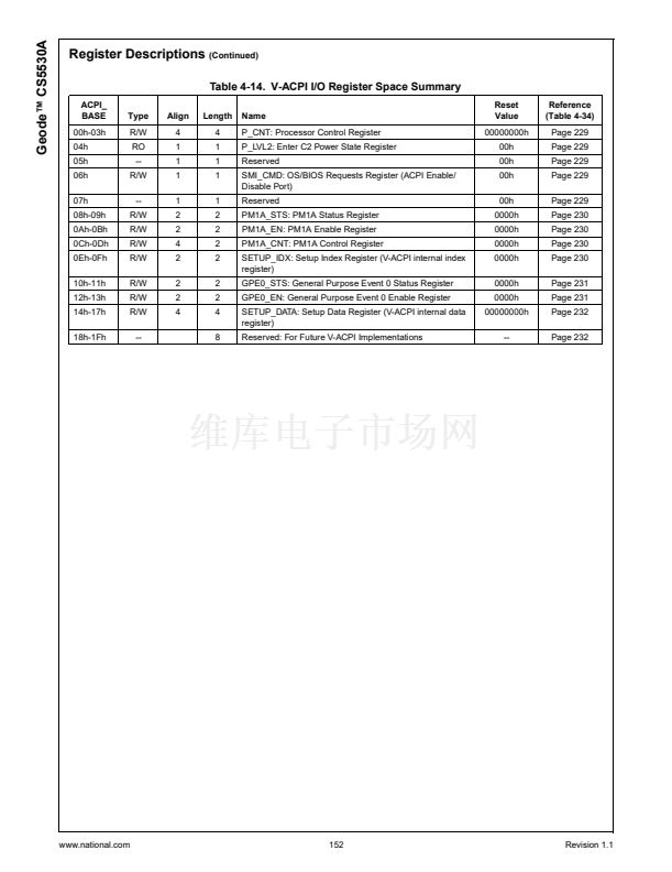
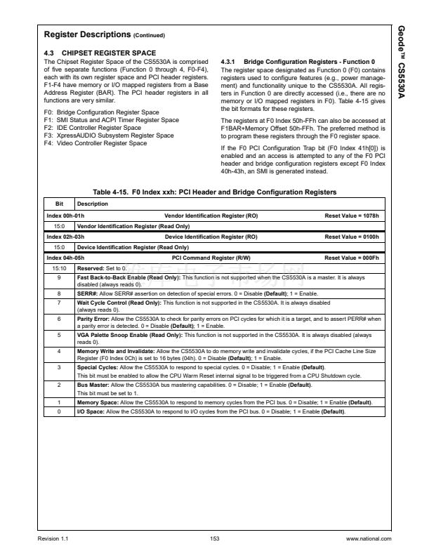
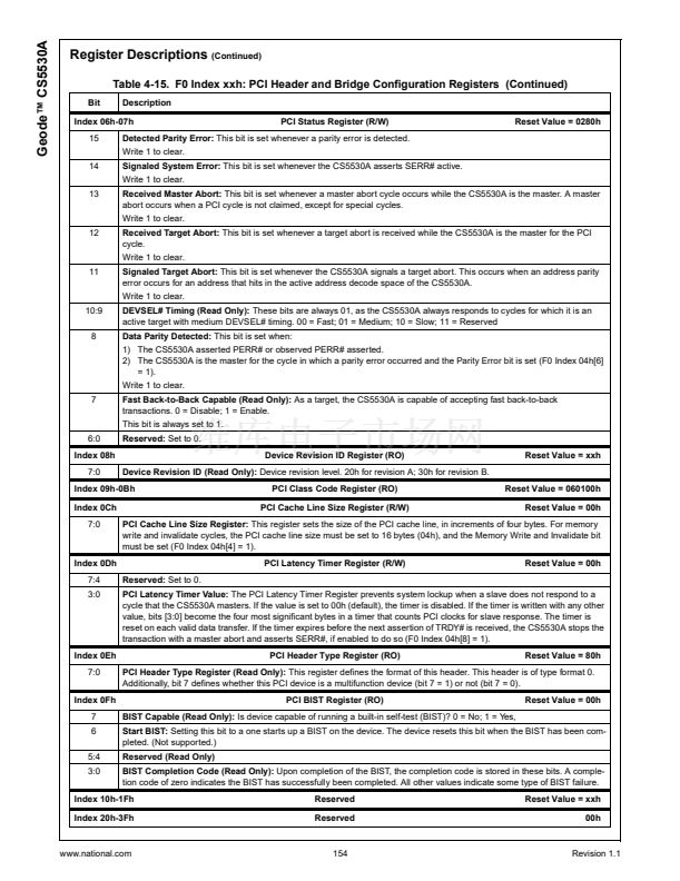
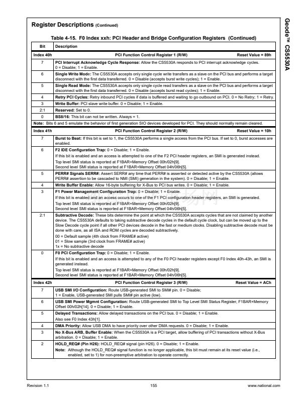
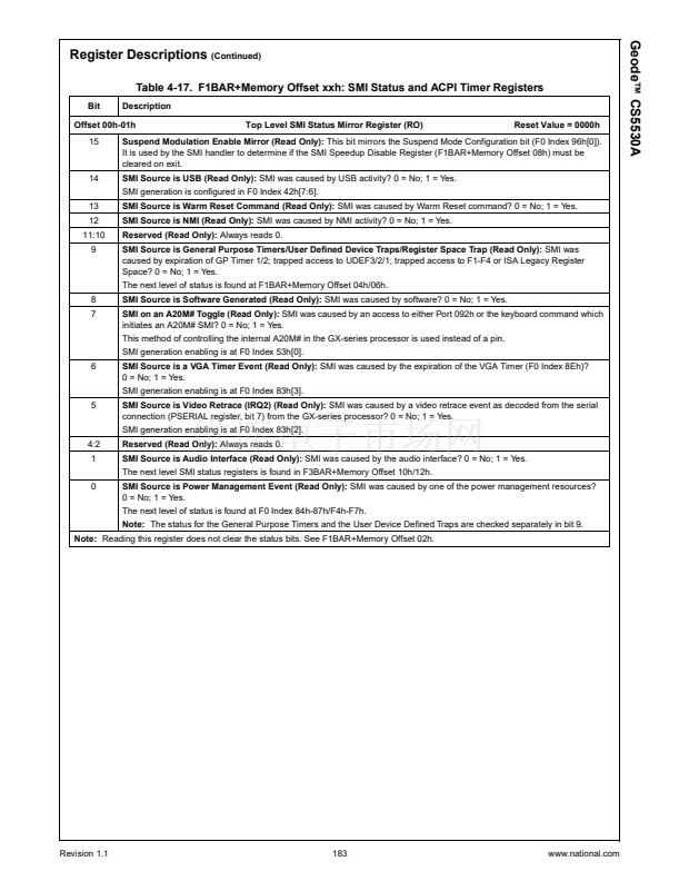
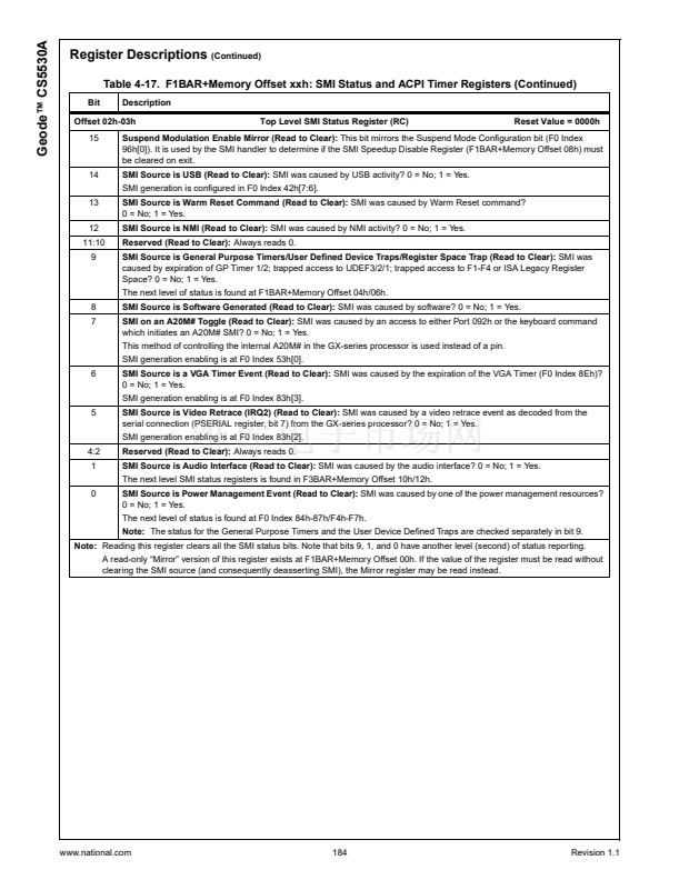
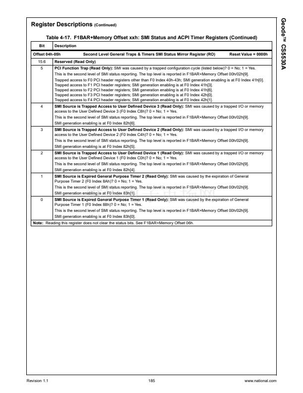
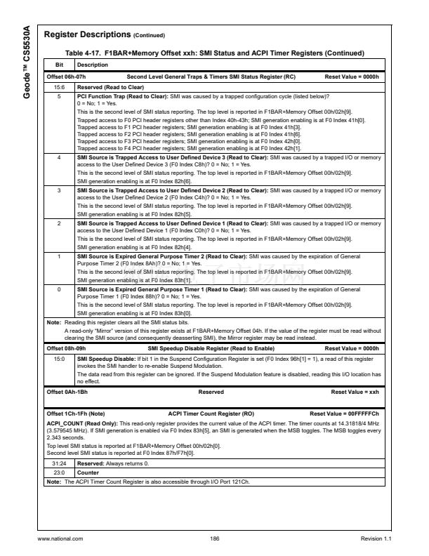
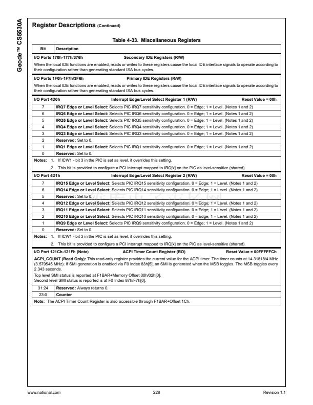
Geode鈩?CS5530A
Functional Description
(Continued)
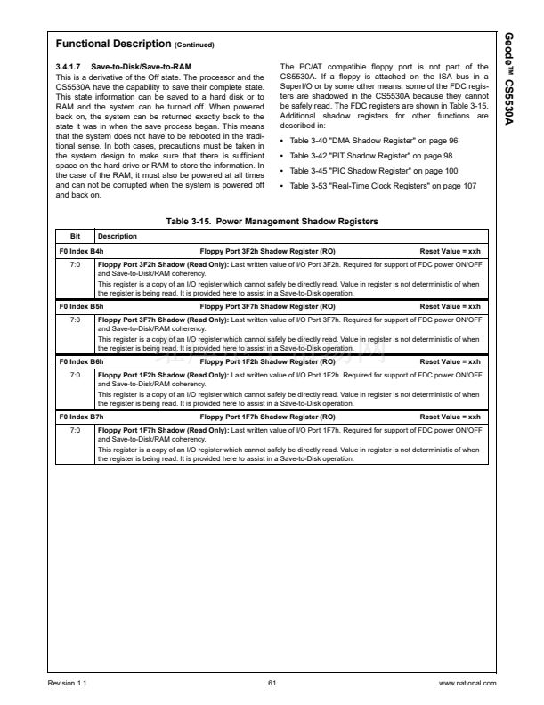
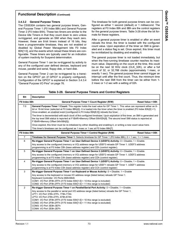
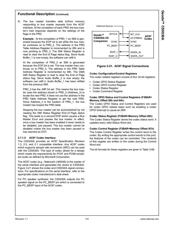
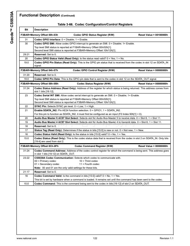
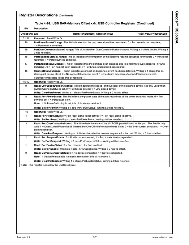
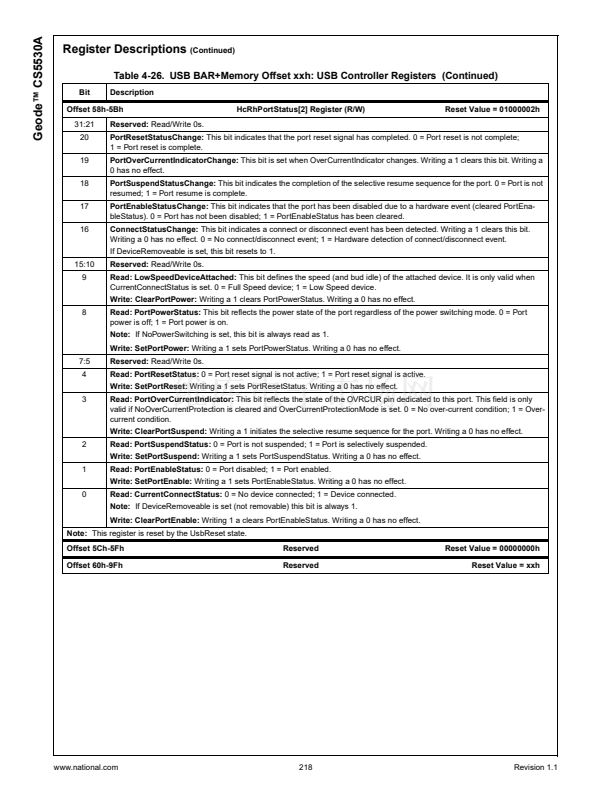
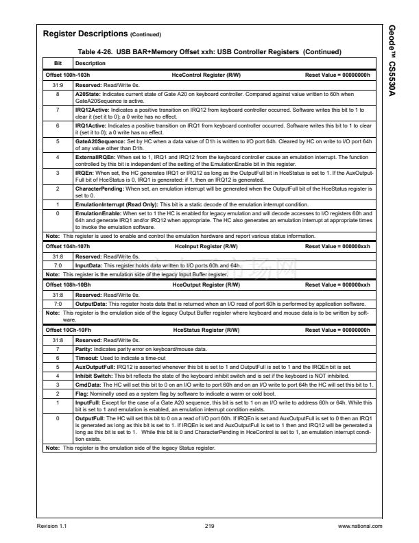
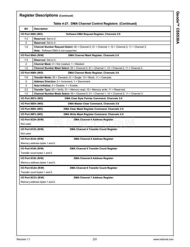
Table 3-32. GPIO Pin Configuration/Control Registers (Continued)
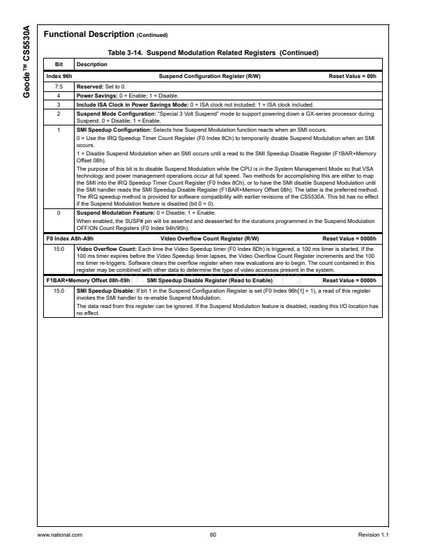
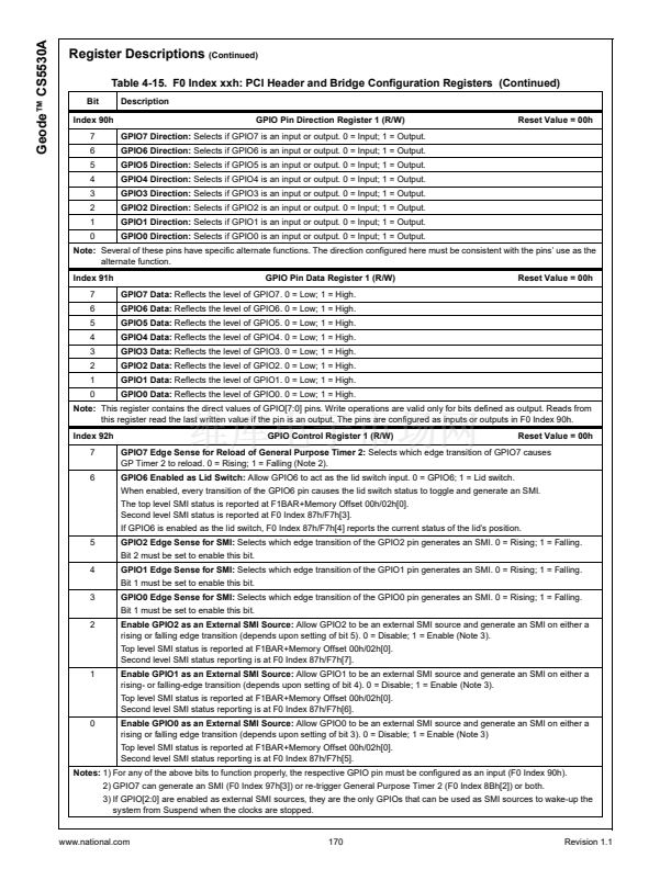
Bit
Description
GPIO Control Register 1 (R/W)
Reset Value = 00h
F0 Index 92h
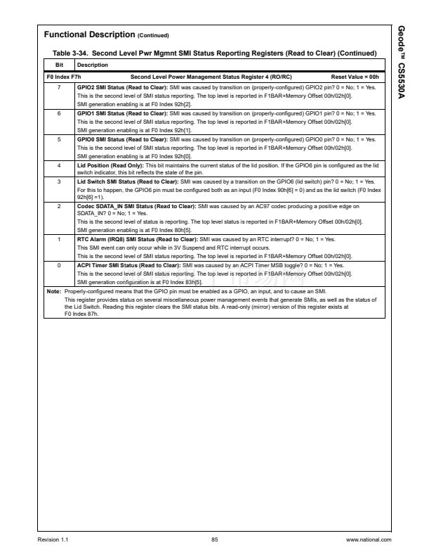
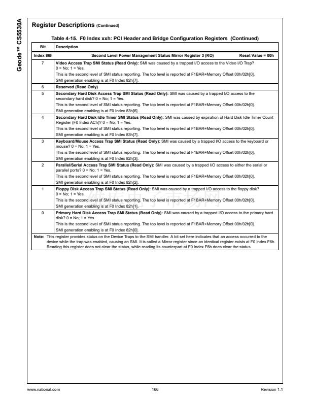
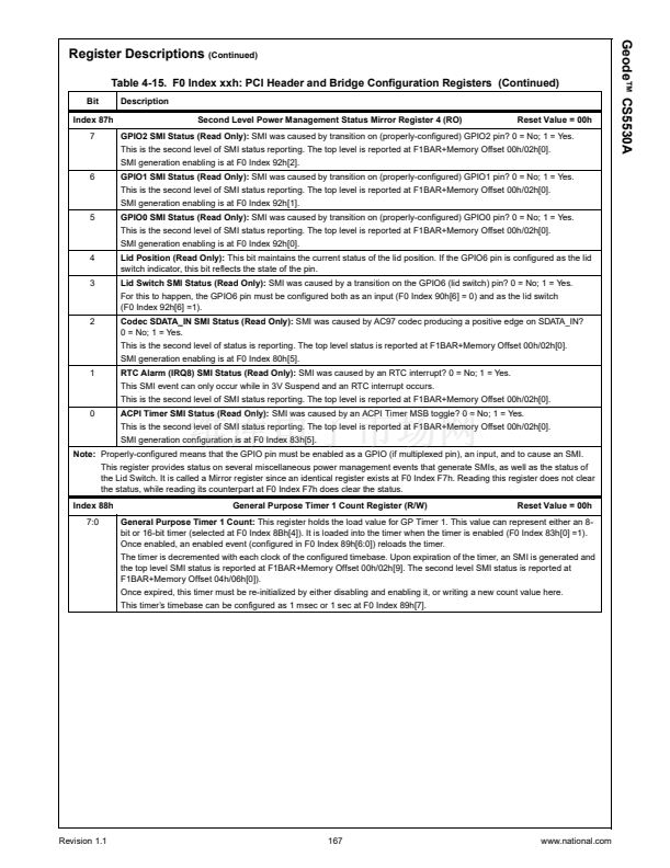
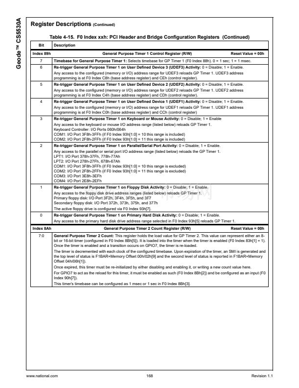
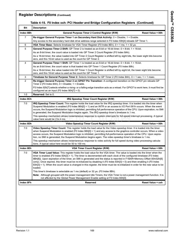
7
6
GPIO7 Edge Sense for Reload of General Purpose Timer 2:
Selects which edge transition of GPIO7 causes
GP Timer 2 to reload. 0 = Rising; 1 = Falling (Note 2).
GPIO6 Enabled as Lid Switch:
Allow GPIO6 to act as the lid switch input. 0 = GPIO6; 1 = Lid switch.
When enabled, every transition of the GPIO6 pin causes the lid switch status to toggle and generate an SMI.
The top level SMI status is reported at F1BAR+Memory Offset 00h/02h[0].
Second level SMI status is reported at F0 Index 87h/F7h[3].
If GPIO6 is enabled as the lid switch, F0 Index 87h/F7h[4] reports the current status of the lid鈥檚 position.
5
4
3
2
GPIO2 Edge Sense for SMI:
Selects which edge transition of the GPIO2 pin generates an SMI. 0 = Rising; 1 = Falling.
Bit 2 must be set to enable this bit.
GPIO1 Edge Sense for SMI:
Selects which edge transition of the GPIO1 pin generates an SMI. 0 = Rising; 1 = Falling.
Bit 1 must be set to enable this bit.
GPIO0 Edge Sense for SMI:
Selects which edge transition of the GPIO0 pin generates an SMI. 0 = Rising; 1 = Falling.
Bit 1 must be set to enable this bit.
Enable GPIO2 as an External SMI Source:
Allow GPIO2 to be an external SMI source and generate an SMI on either a
rising or falling edge transition (depends upon setting of bit 5). 0 = Disable; 1 = Enable (Note 3).
Top level SMI status is reported at F1BAR+Memory Offset 00h/02h[0].
Second level SMI status reporting is at F0 Index 87h/F7h[7].
1
Enable GPIO1 as an External SMI Source:
Allow GPIO1 to be an external SMI source and generate an SMI on either a
rising- or falling-edge transition (depends upon setting of bit 4). 0 = Disable; 1 = Enable (Note 3).
Top level SMI status is reported at F1BAR+Memory Offset 00h/02h[0].
Second level SMI status reporting is at F0 Index 87h/F7h[6].
0
Enable GPIO0 as an External SMI Source:
Allow GPIO0 to be an external SMI source and generate an SMI on either a
rising or falling edge transition (depends upon setting of bit 3). 0 = Disable; 1 = Enable (Note 3)
Top level SMI status is reported at F1BAR+Memory Offset 00h/02h[0].
Second level SMI status reporting is at F0 Index 87h/F7h[5].
Notes:
1) For any of the above bits to function properly, the respective GPIO pin must be configured as an input (F0 Index 90h).
2) GPIO7 can generate an SMI (F0 Index 97h[3]) or re-trigger General Purpose Timer 2 (F0 Index 8Bh[2]) or both.
3) If GPIO[2:0] are enabled as external SMI sources, they are the only GPIOs that can be used as SMI sources to wake-up the
system from Suspend when the clocks are stopped.
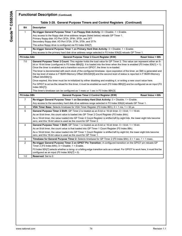
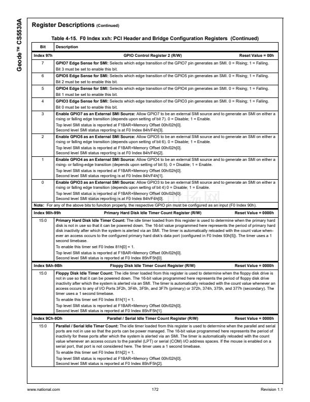
F0 Index 97h
7
6
5
4
3
Bit 3 must be set to enable this bit.
GPIO5 Edge Sense for SMI:
Selects which edge transition of the GPIO5 pin generates an SMI. 0 = Rising; 1 = Falling.
Bit 2 must be set to enable this bit.
GPIO4 Edge Sense for SMI:
Selects which edge transition of the GPIO4 pin generates an SMI. 0 = Rising; 1 = Falling.
Bit 1 must be set to enable this bit.
GPIO3 Edge Sense for SMI:
Selects which edge transition of the GPIO3 pin generates an SMI. 0 = Rising; 1 = Falling.
Bit 0 must be set to enable this bit.
Enable GPIO7 as an External SMI Source:
Allow GPIO7 to be an external SMI source and to generate an SMI on either a
rising or falling edge transition (depends upon setting of bit 7). 0 = Disable; 1 = Enable.
Top level SMI status is reported at F1BAR+Memory Offset 00h/02h[0].
Second level SMI status reporting is at F0 Index 84h/F4h[3].
2
Enable GPIO5 as an External SMI Source:
Allow GPIO5 to be an external SMI source and to generate an SMI on either a
rising or falling edge transition (depends upon setting of bit 6). 0 = Disable; 1 = Enable.
Top level SMI status is reported at F1BAR+Memory Offset 00h/02h[0].
Second level SMI status reporting is at F0 Index 84h/F4h[2].
1
Enable GPIO4 as an External SMI Source:
Allow GPIO4 to be an external SMI source and to generate an SMI on either a
rising- or falling-edge transition (depends upon setting of bit 5). 0 = Disable; 1 = Enable.
Top level SMI status is reported at F1BAR+Memory Offset 00h/02h[0].
Second level SMI status reporting is at F0 Index 84h/F4h[1].
GPIO Control Register 2 (R/W)
Reset Value = 00h
GPIO7 Edge Sense for SMI:
Selects which edge transition of the GPIO7 pin generates an SMI. 0 = Rising; 1 = Falling.
Revision 1.1
77
www.national.com


 1
1
 2
2
 3
3
 4
4
 5
5
 6
6
 7
7
 8
8
 9
9
 10
10
 11
11
 12
12
 13
13
 14
14
 15
15
 16
16
 17
17
 18
18
 19
19
 20
20
 21
21
 22
22
 23
23
 24
24
 25
25
 26
26
 27
27
 28
28
 29
29
 30
30
 31
31
 32
32
 33
33
 34
34
 35
35
 36
36
 37
37
 38
38
 39
39
 40
40
 41
41
 42
42
 43
43
 44
44
 45
45
 46
46
 47
47
 48
48
 49
49
 50
50
 51
51
 52
52
 53
53
 54
54
 55
55
 56
56
 57
57
 58
58
 59
59
 60
60
 61
61
 62
62
 63
63
 64
64
 65
65
 66
66
 67
67
 68
68
 69
69
 70
70
 71
71
 72
72
 73
73
 74
74
 75
75
 76
76
 77
77
 78
78
 79
79
 80
80
 81
81
 82
82
 83
83
 84
84
 85
85
 86
86
 87
87
 88
88
 89
89
 90
90
 91
91
 92
92
 93
93
 94
94
 95
95
 96
96
 97
97
 98
98
 99
99
 100
100
 101
101
 102
102
 103
103
 104
104
 105
105
 106
106
 107
107
 108
108
 109
109
 110
110
 111
111
 112
112
 113
113
 114
114
 115
115
 116
116
 117
117
 118
118
 119
119
 120
120
 121
121
 122
122
 123
123
 124
124
 125
125
 126
126
 127
127
 128
128
 129
129
 130
130
 131
131
 132
132
 133
133
 134
134
 135
135
 136
136
 137
137
 138
138
 139
139
 140
140
 141
141
 142
142
 143
143
 144
144
 145
145
 146
146
 147
147
 148
148
 149
149
 150
150
 151
151
 152
152
 153
153
 154
154
 155
155
 156
156
 157
157
 158
158
 159
159
 160
160
 161
161
 162
162
 163
163
 164
164
 165
165
 166
166
 167
167
 168
168
 169
169
 170
170
 171
171
 172
172
 173
173
 174
174
 175
175
 176
176
 177
177
 178
178
 179
179
 180
180
 181
181
 182
182
 183
183
 184
184
 185
185
 186
186
 187
187
 188
188
 189
189
 190
190
 191
191
 192
192
 193
193
 194
194
 195
195
 196
196
 197
197
 198
198
 199
199
 200
200
 201
201
 202
202
 203
203
 204
204
 205
205
 206
206
 207
207
 208
208
 209
209
 210
210
 211
211
 212
212
 213
213
 214
214
 215
215
 216
216
 217
217
 218
218
 219
219
 220
220
 221
221
 222
222
 223
223
 224
224
 225
225
 226
226
 227
227
 228
228
 229
229
 230
230
 231
231
 232
232
 233
233
 234
234
 235
235
 236
236
 237
237
 238
238
 239
239
 240
240
 241
241
 242
242
 243
243
 244
244
 245
245
 246
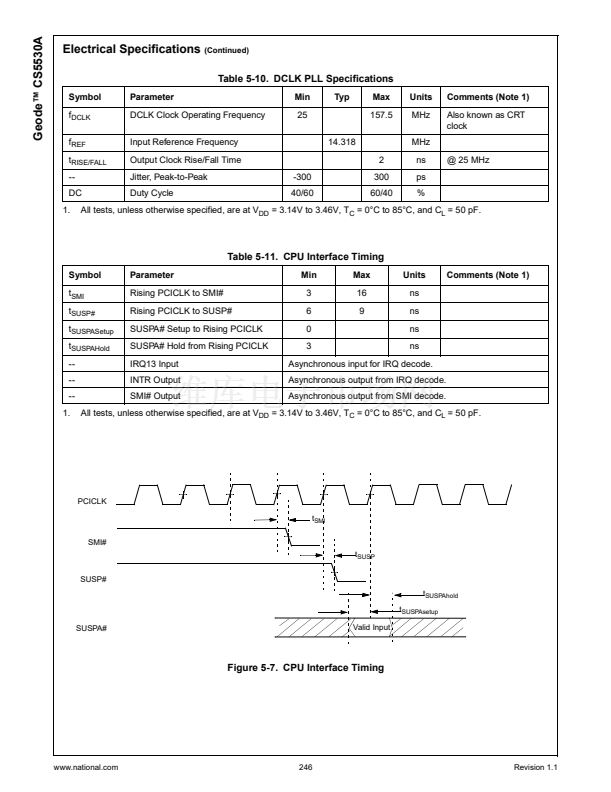
246
 247
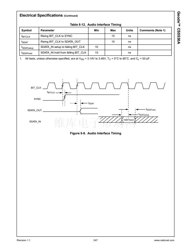
247
 248
248
 249
249
 250
250
 251
251
 252
252
 253
253
 254
254
 255
255
 256
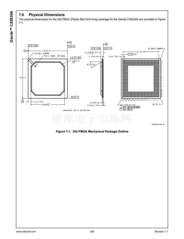
256
 257
257
 258
258
 259
259
