endpoint data buffers and the codec port interface. The USB endpoint number and direction can be programmed for
each DMA channel. Also, the codec port interface time slots to be serviced by each DMA channel can be
programmed.
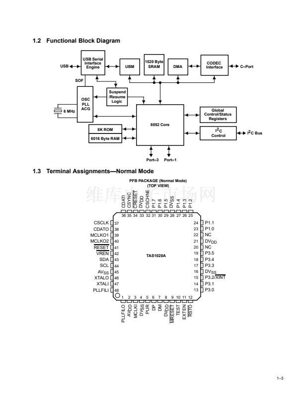
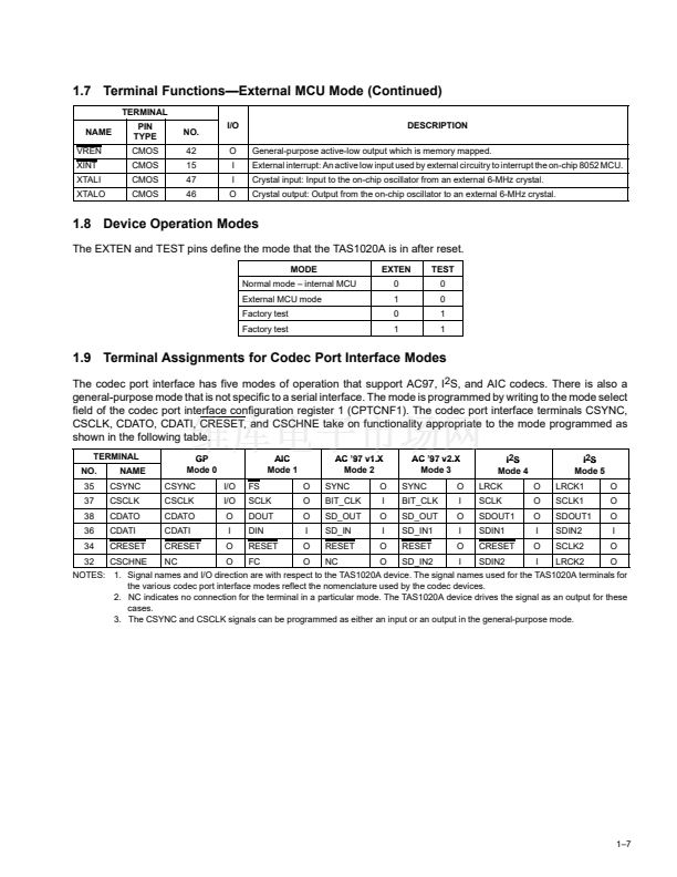
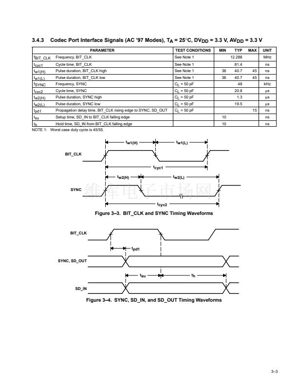
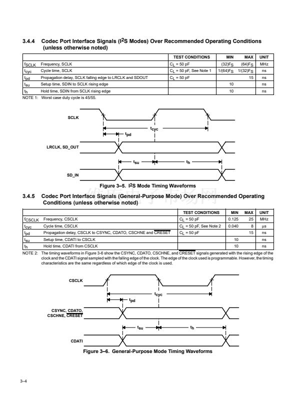
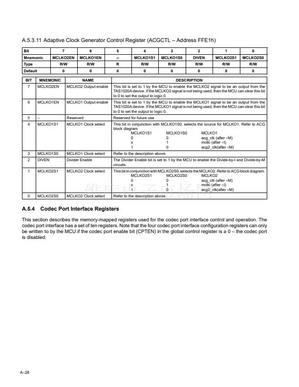
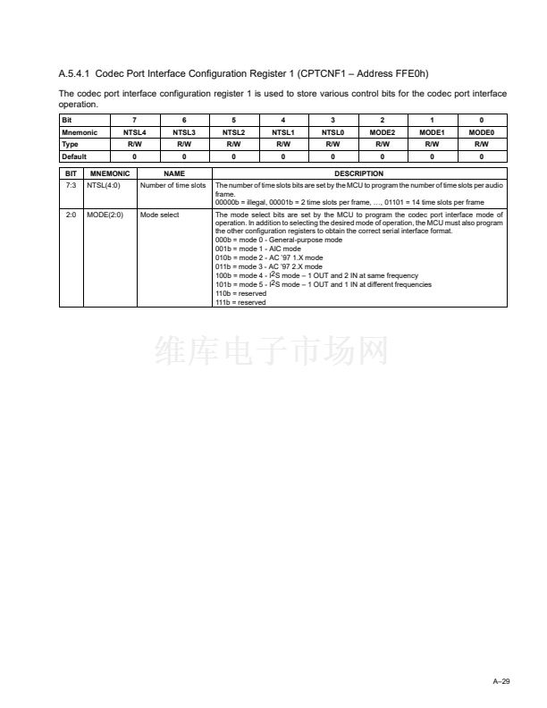
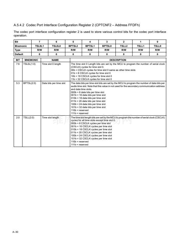
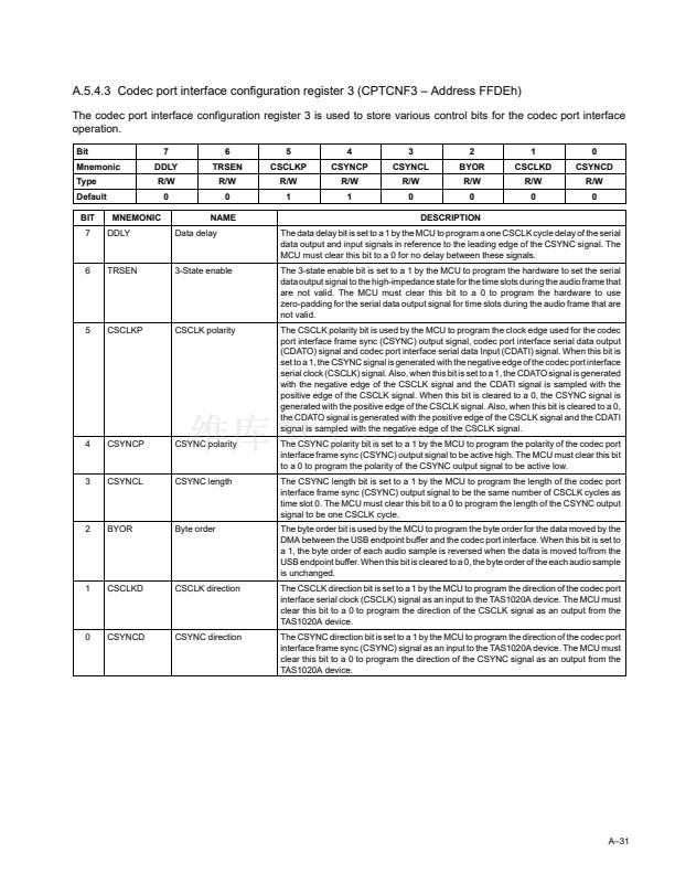
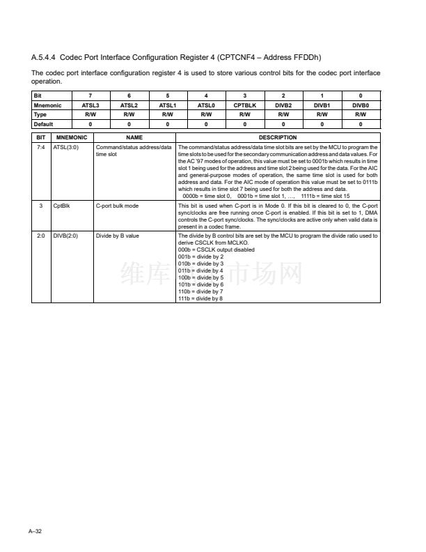
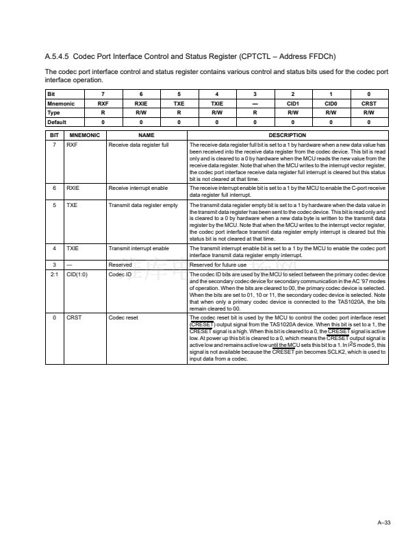
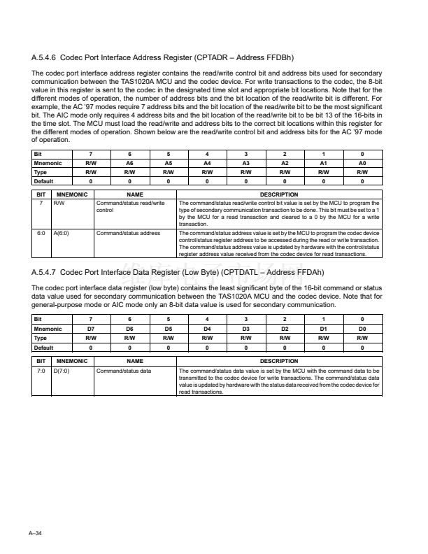
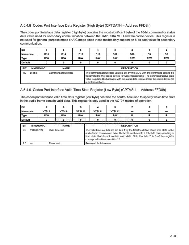
2.1.13 Codec Port Interface
The TAS1020A provides a configurable full duplex bidirectional serial interface that can be used to connect to a codec
or other external device types for streaming USB isochronous data. The interface can be configured to support
several different industry standard protocols, including AC 鈥?7 1.X, AC 鈥?7 2.X, AIC, and I
2
S. The TAS1020A also has
a general-purpose mode to support other protocols.
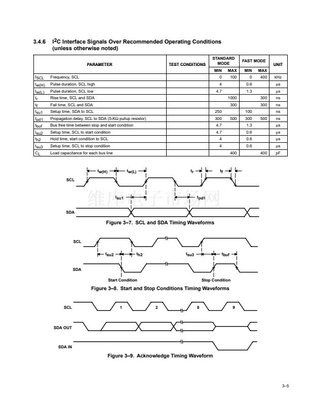
2.1.14 I
2
C Interface
The I
2
C interface logic provides a two-wire serial interface that the 8052 MCU can use to access other ICs. The
TAS1020A is an I
2
C master device only and supports single byte or multiple byte read and write operations. The
interface can be programmed to operate at either 100 kbps or 400 kbps. In addition, the protocol supports 8-bit or
16-bit addressing for accessing the I
2
C slave device memory locations. The TAS1020A supports I
2
C wait states. This
means slaves can assert wait state on the I
2
C bus by pulling the SCL line low.
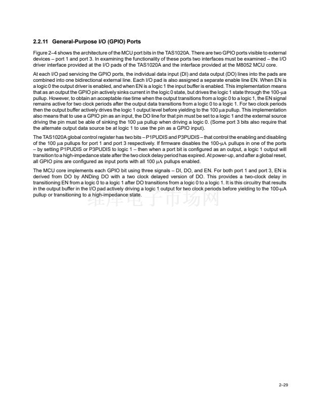
2.1.15 General
-
Purpose IO Ports (GPIO)
The TAS1020A provides two general-purpose IO ports that are controlled by the internal 8052 MCU. The two ports
are port 1 and port 3. Port 1 provides true GPIO capability. Each bit of port 1 can be independently used as either
an input or output, and consists of an output buffer, an input buffer, and a pullup resistor. Some of the bits of port 3
also provide true GPIO capability, but, in addition, some of the bits of port 3 also provide alternate input and output
uses. An example of this is P3.2, which is used as the external interrupt (XINT) input to the TAS1020A. A detailed
description of the alternate uses of some of the port 3 bits is presented in Section 2.2.11.
The pullup resistors for port 1 and port 3 can be disabled by bits P1PUDIS and P3PUDIS respectively in the on-chip
register GLOBCTL. In addition, any port 3 pin can be used to wake up the host PC from a low-power suspend mode.
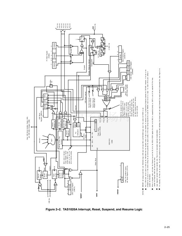
2.1.16 Interrupt Logic
The interrupt logic monitors the various conditions that can cause an interrupt and asserts the interrupt 0 (INTO) input
on the 8052 MCU core accordingly. All of the TAS1020A internal interrupt sources and the external interrupt (XINT)
input are ORed together to generate the INT0 signal. An interrupt vector register is used by the MCU to identify the
interrupt source.
2.1.17 Reset Logic
An external master reset (MRESET) input signal that is asynchronous to the internal clocks can be used to reset the
TAS1020A logic. In addition to this master reset, the TAS1020A logic can also be reset by a USB reset from the host
PC if bit FRSTE in the on-chip register USBCTL is set to 1. The TAS1020A also provides a reset output (RSTO) signal
that can be used by external devices. This signal is asserted when either a master reset occurs or when a USB reset
occurs and FRSTE is set to 1.
2.2 Device Operation
The operation of the TAS1020A is explained in the following sections. For additional information on USB, refer to the
Universal Serial Bus Specification, Version 1.1.
2鈥?


 1
1
 2
2
 3
3
 4
4
 5
5
 6
6
 7
7
 8
8
 9
9
 10
10
 11
11
 12
12
 13
13
 14
14
 15
15
 16
16
 17
17
 18
18
 19
19
 20
20
 21
21
 22
22
 23
23
 24
24
 25
25
 26
26
 27
27
 28
28
 29
29
 30
30
 31
31
 32
32
 33
33
 34
34
 35
35
 36
36
 37
37
 38
38
 39
39
 40
40
 41
41
 42
42
 43
43
 44
44
 45
45
 46
46
 47
47
 48
48
 49
49
 50
50
 51
51
 52
52
 53
53
 54
54
 55
55
 56
56
 57
57
 58
58
 59
59
 60
60
 61
61
 62
62
 63
63
 64
64
 65
65
 66
66
 67
67
 68
68
 69
69
 70
70
 71
71
 72
72
 73
73
 74
74
 75
75
 76
76
 77
77
 78
78
 79
79
 80
80
 81
81
 82
82
 83
83
 84
84
 85
85
 86
86
 87
87
 88
88
 89
89
 90
90
 91
91
 92
92
 93
93
 94
94
 95
95
 96
96
 97
97
 98
98
 99
99
 100
100
 101
101
 102
102
 103
103
 104
104
 105
105
 106
106
 107
107
 108
108
 109
109
 110
110
 111
111
 112
112
 113
113
 114
114
