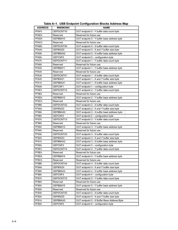
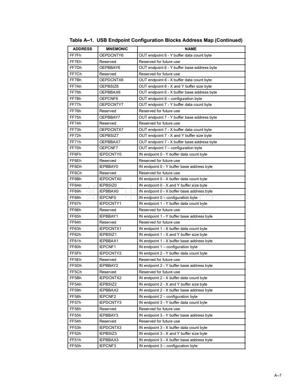
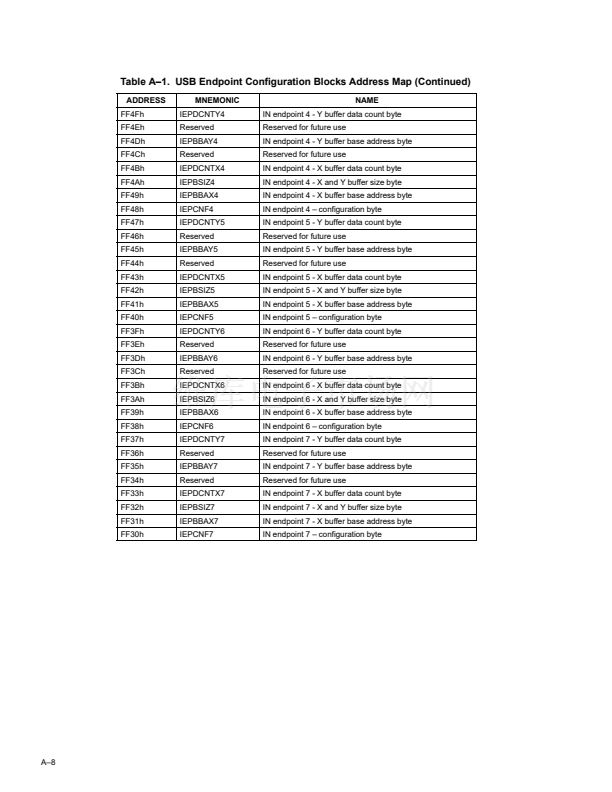
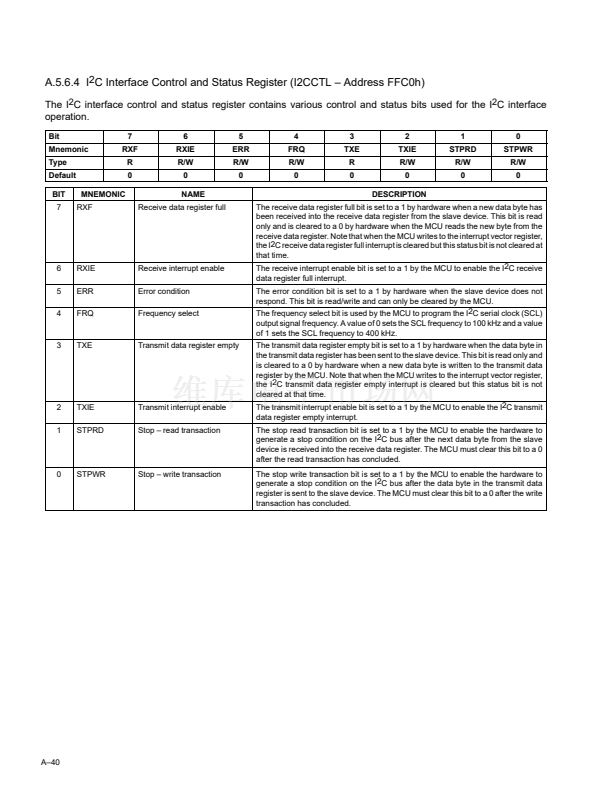
suspend state has been active for at least 5 ms. In addition, the specification requires that the remote wake-up resume
signaling be generated for at least 1ms but for no more than 15 ms. The 5 ms requirement is met by not entering the
suspend mode until an idle state, or j state, is detected, uninterrupted, for 5 ms. The RWUP pulse results in driving
a k state onto the USB bus for 1 to 2 ms, and thus the 15 ms requirement is also met. Moreover, if an application wishes
to extend the duration of the k state on the USB bus, it need only extend the pulse width of RWUP. The resulting
duration of the resume signaling is the duration of the RWUP pulse plus 1 to 2 ms.
The condition that activates a remote wake-up is a transition from 1 to 0 on one of the P3 port bits whose
corresponding mask bit has been set to zero. (When in the suspend mode, the XINT input is treated as port bit P3.2).
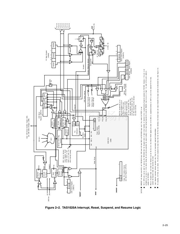
As seen in Figure 2鈥?, the P3 mask register bits are gated with the P3 port input lines from the I/O port cells. The
gated P3 port bits are then all ORed together and the output is ANDed with the suspend signal. The output of this
logic drives the clock input of a flip-flop, and when the output of this logic transitions from 0 to 1, the flip-flop is set
to 1. The setting of this flip-flop to 1 results in the TAS1020A exiting the suspend state and resuming all clocks,
including those to the MCU core. The output of this flip-flop is also gated with bit XINTEN in the global control register
GLOBCTL, and the output of this gate drives the INT0 interrupt logic. This means that a remote wake-up generates
an INT0 interrupt to the MCU only if bit XINTEN has been set. Therefore, before entering a suspend state, the firmware
must set XINTEN if remote wake-up capability is to be enabled.
The wake-up interrupt is seen by the firmware as an XINT interrupt; that is, the interrupt vector register VECINT has
an output value of 0x1F. If the XINT pin is to be used as an event marker during normal operation, and if one of the
P3 port bits is to be used for a wake-up interrupt, the firmware must be able to distinguish between a wake-up interrupt
and a normal XINT interrupt. One technique would be to examine the state of the IDL bit in the MCU power control
register. If this bit is set, the interrupt event is a wake-up interrupt; otherwise, the interrupt is a normal XINT interrupt.
If an XINT event should occur during a suspend mode, the event is ignored if the mask bit for P3.2 is set. (During a
suspend mode the TAS1020A clocks are disabled, and thus an incoming XINT interrupt event does not propagate
through the synchronization logic and activate the MCU INT0 input).
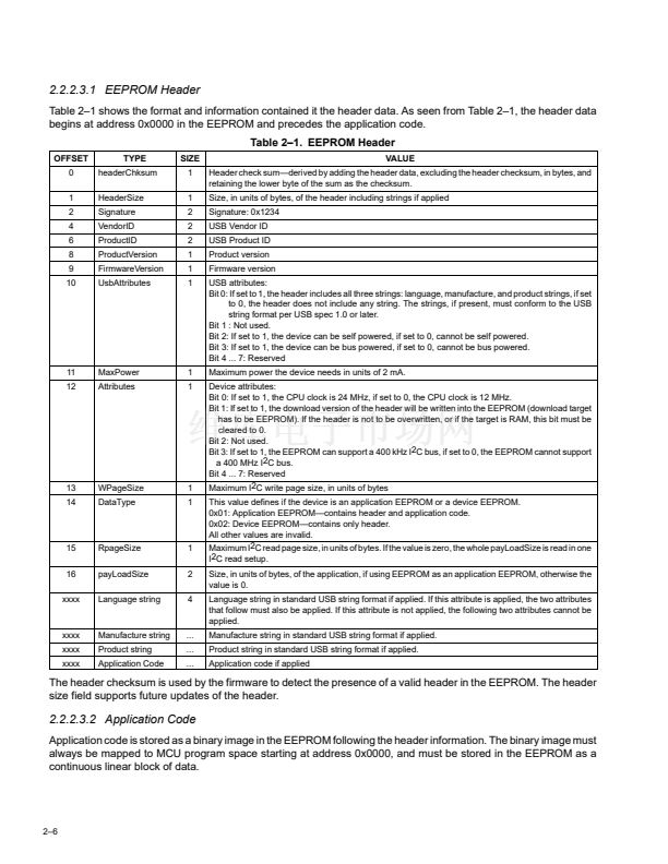
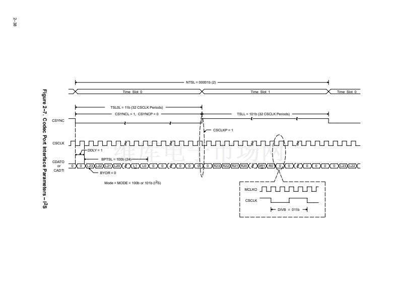
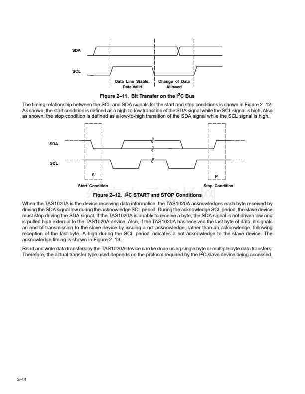
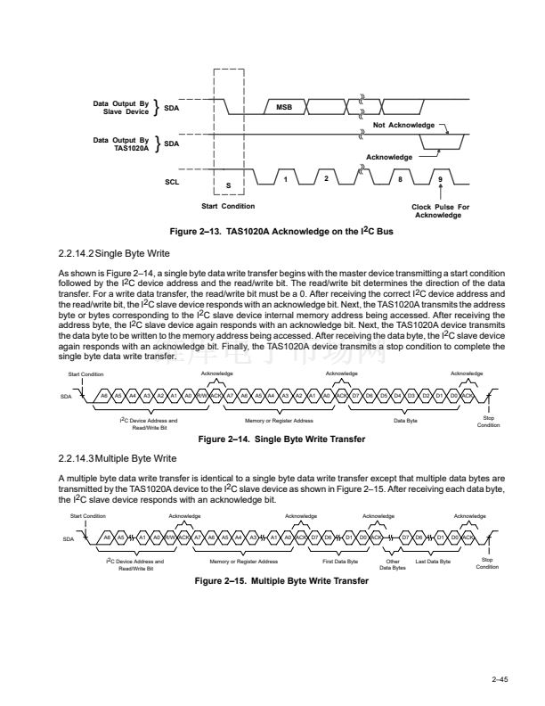
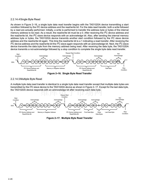
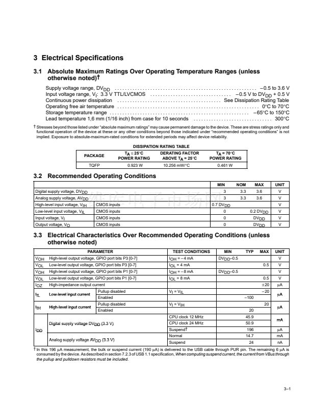
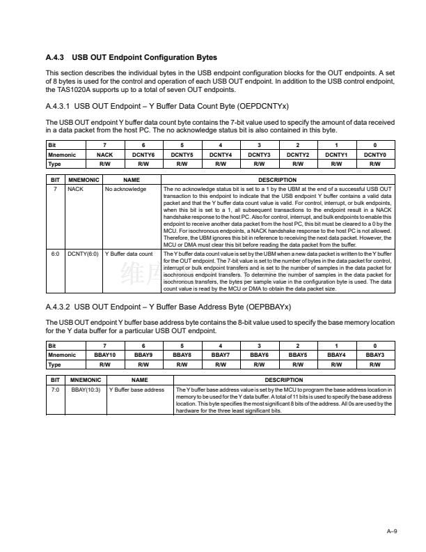
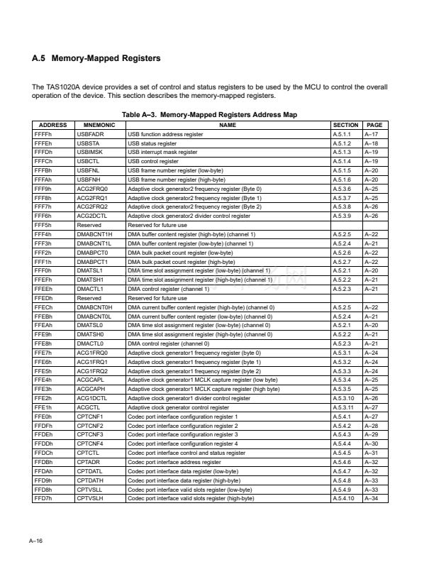
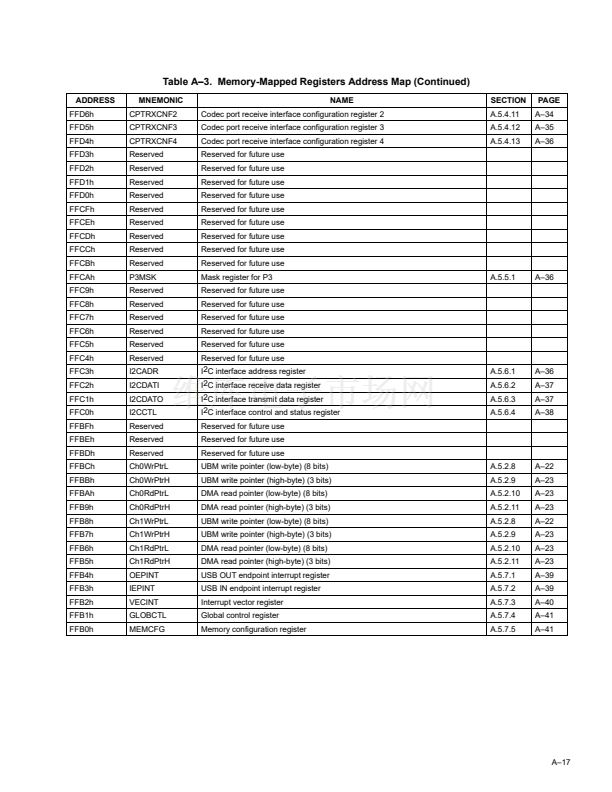
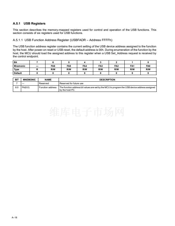
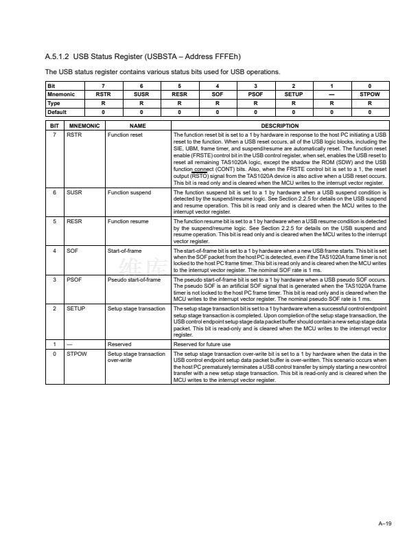
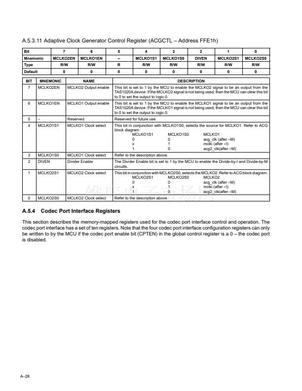
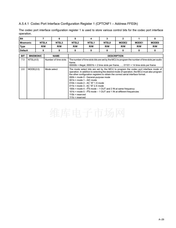
2.2.6
Adaptive Clock Generator (ACG)
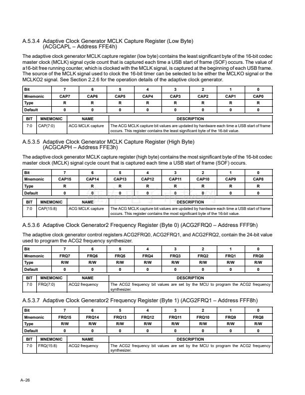
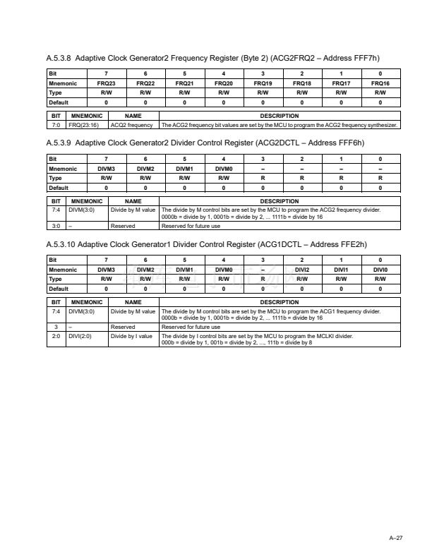
The adaptive clock generator is used to generate two programmable master clock output signals (MCLKO and
MCLKO2) that can be used by the codec port interface and the codec device. Two separate and programmable
frequency synthesizers provide the two master clocks. This allows the TAS1020A to support different record and
playback rates for those devices that require separate master clocks to implement different rates. For isochronous
transactions, the ACG can also support USB asynchronous, synchronous, and adaptive modes of operation. The
ACG keeps count of the number of master clock events between USB SOF time marks, and the DCNTX/Y field of
the endpoint register IEPDCNTX/Y keeps track of the number of samples received between USB SOF time marks.
Synchronous isochronous operation can be accomplished by adjusting one of the two frequency synthesizers until
the correct number of master clock events is obtained between USB SOF time marks. Similarly, monitoring the
number of samples received between USB SOF events can accommodate adaptive isochronous operation. Here the
frequency synthesizer is adjusted to obtain the proper codec output rate for the number of samples received. The
TAS1020A can also accommodate asynchronous isochronous operation, and the input MCLKI is provided for this
case. For asynchronous isochronous operation, the external clock pin MCLKI is used to derive the data and sync
signal to the codec. However, the external clock that provides the input to pin MCLKI, instead of the master clock
output (MCLKO or MCLKO2) from the ACG, must also source the codec鈥檚 MCLK.
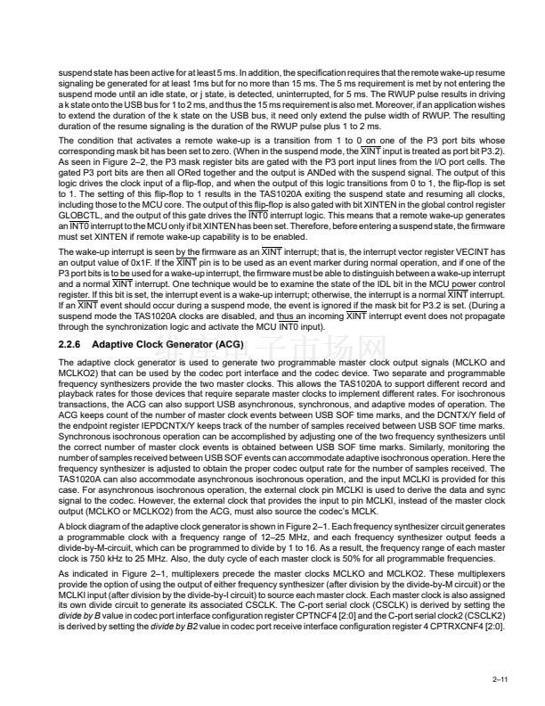
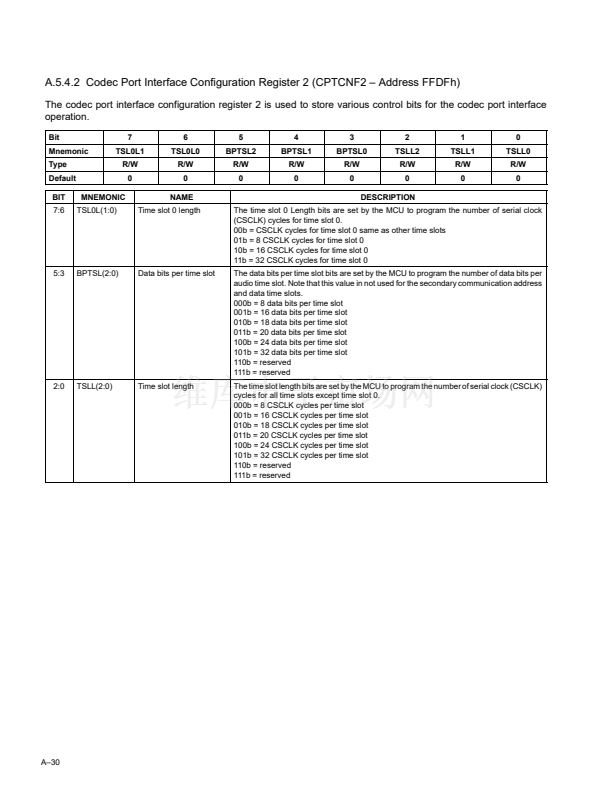
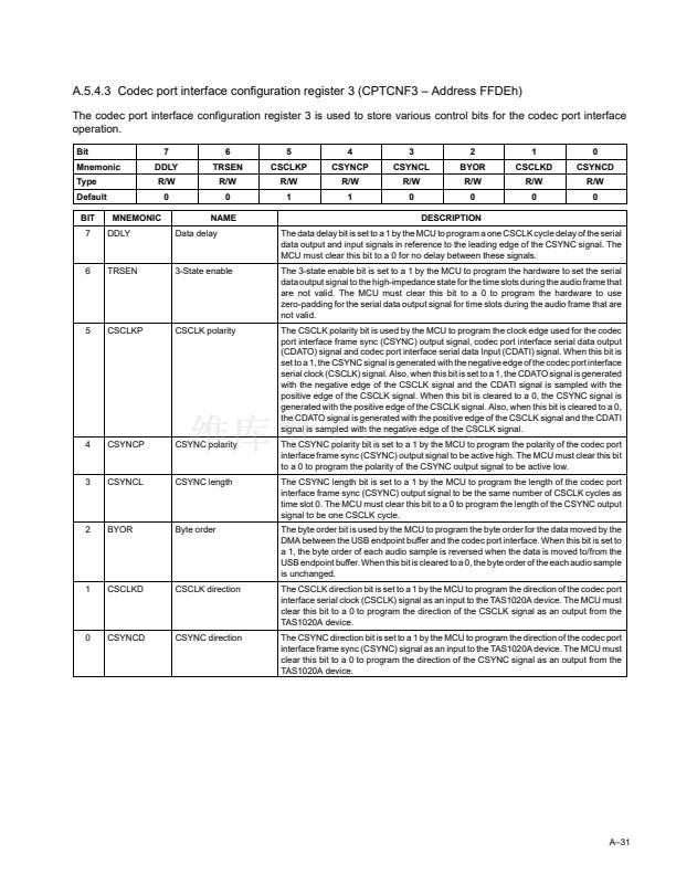
A block diagram of the adaptive clock generator is shown in Figure 2鈥?. Each frequency synthesizer circuit generates
a programmable clock with a frequency range of 12鈥?5 MHz, and each frequency synthesizer output feeds a
divide-by-M-circuit, which can be programmed to divide by 1 to 16. As a result, the frequency range of each master
clock is 750 kHz to 25 MHz. Also, the duty cycle of each master clock is 50% for all programmable frequencies.
As indicated in Figure 2鈥?, multiplexers precede the master clocks MCLKO and MCLKO2. These multiplexers
provide the option of using the output of either frequency synthesizer (after division by the divide-by-M circuit) or the
MCLKI input (after division by the divide-by-I circuit) to source each master clock. Each master clock is also assigned
its own divide circuit to generate its associated CSCLK. The C-port serial clock (CSCLK) is derived by setting the
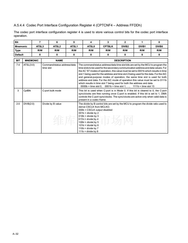
divide by B
value in codec port interface configuration register CPTNCF4 [2:0] and the C-port serial clock2 (CSCLK2)
is derived by setting the
divide by B2
value in codec port receive interface configuration register 4 CPTRXCNF4 [2:0].
2鈥?1


 1
1
 2
2
 3
3
 4
4
 5
5
 6
6
 7
7
 8
8
 9
9
 10
10
 11
11
 12
12
 13
13
 14
14
 15
15
 16
16
 17
17
 18
18
 19
19
 20
20
 21
21
 22
22
 23
23
 24
24
 25
25
 26
26
 27
27
 28
28
 29
29
 30
30
 31
31
 32
32
 33
33
 34
34
 35
35
 36
36
 37
37
 38
38
 39
39
 40
40
 41
41
 42
42
 43
43
 44
44
 45
45
 46
46
 47
47
 48
48
 49
49
 50
50
 51
51
 52
52
 53
53
 54
54
 55
55
 56
56
 57
57
 58
58
 59
59
 60
60
 61
61
 62
62
 63
63
 64
64
 65
65
 66
66
 67
67
 68
68
 69
69
 70
70
 71
71
 72
72
 73
73
 74
74
 75
75
 76
76
 77
77
 78
78
 79
79
 80
80
 81
81
 82
82
 83
83
 84
84
 85
85
 86
86
 87
87
 88
88
 89
89
 90
90
 91
91
 92
92
 93
93
 94
94
 95
95
 96
96
 97
97
 98
98
 99
99
 100
100
 101
101
 102
102
 103
103
 104
104
 105
105
 106
106
 107
107
 108
108
 109
109
 110
110
 111
111
 112
112
 113
113
 114
114
