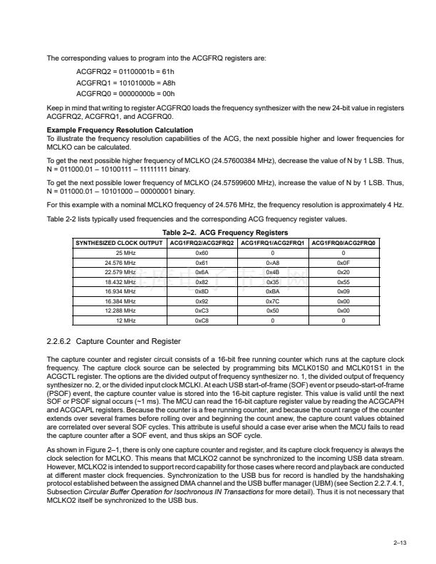
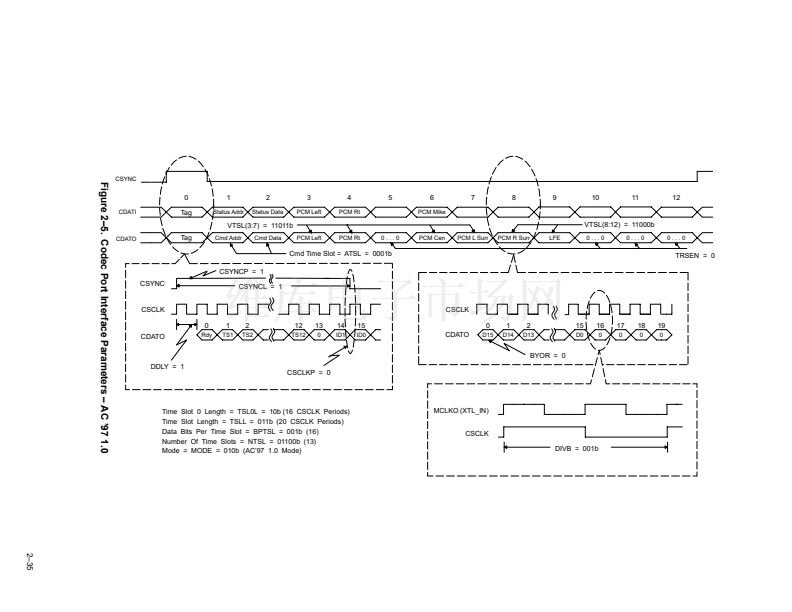
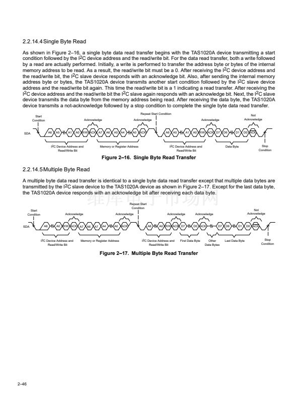
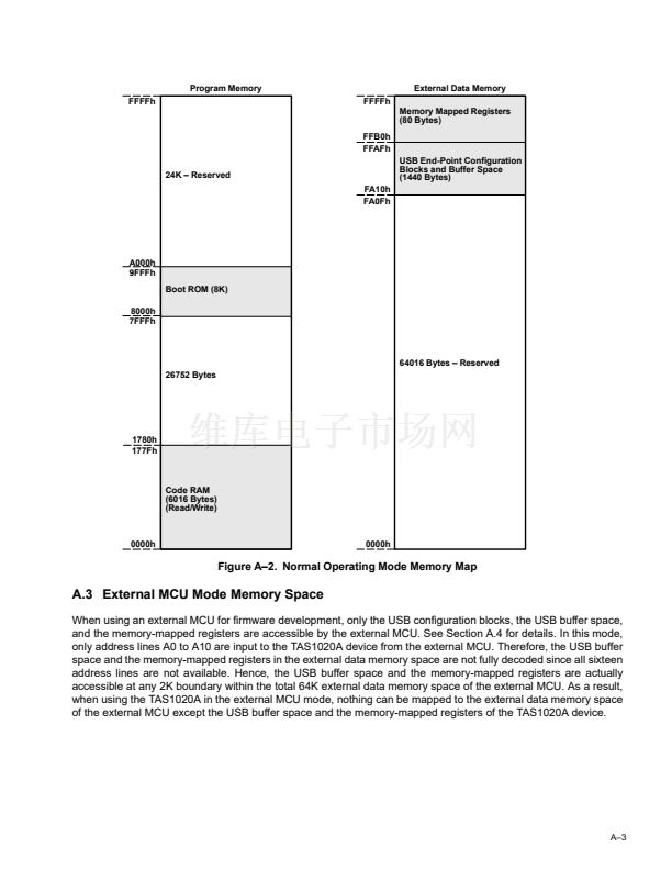
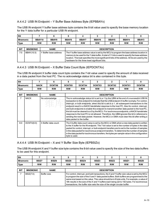
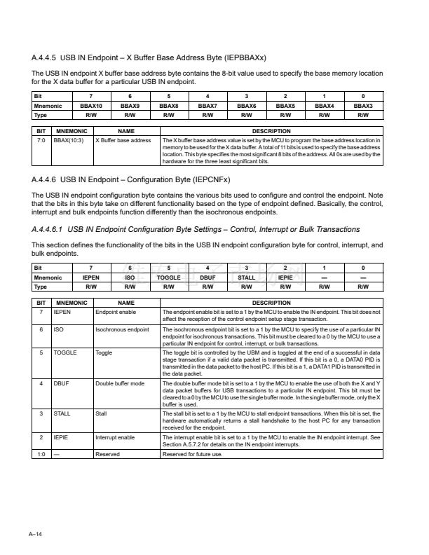
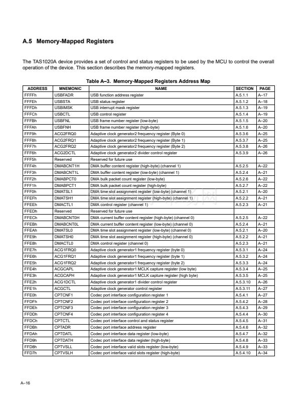
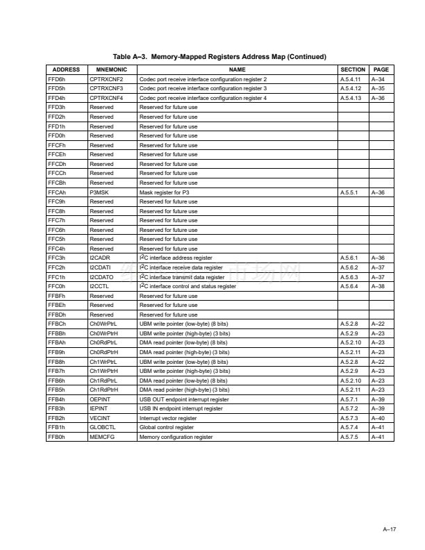
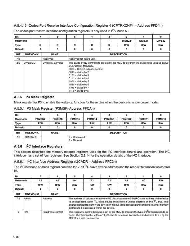
In both modes, the on-chip C-port is used to output the received bulk data to an external device. To implement
DMA-supported transactions, the C-port must be programmed to operate in either a general-purpose (GP) mode or
an Audio Codec 鈥?7 (AC97) mode. When in the general-purpose mode, SYNC is disabled when there is no valid data
in the buffer to be output; in the AC97 mode, the time slot
valid
bits in the tag field are disabled when there is no valid
data in the buffer to be output.
Software Handshake Using MCU, UBM, and External Device
Bulk data has the lowest priority of all transfers on the USB bus. But when there is little other activity on the USB bus,
bulk transfers can achieve significant transfer rates. Bulk transfer rates then can fluctuate greatly, and for this reason
it is sometimes necessary to monitor the transfer rate of bulk transfers in order to throttle back the transfer rate when
the rate exceeds the bandwidth of the target device. The software handshake mode is provided to enable the
implementation of just such a
throttling
of data.
The following steps explain the operation of the software handshake mode.
1. The MCU initializes one of the OUT endpoints as a bulk OUT endpoint by programming the appropriate USB
endpoint configuration block. This entails programming the buffer size and buffer base address, selecting
the buffer mode, enabling the endpoint interrupt, initializing the toggle bit, enabling the endpoint, and
clearing the NACK bit.
2. To configure a given DMA channel to process a given endpoint in a software handshake mode, the MCU
must
鈥?/div>
Enable the handshake mode by setting the HSKEN bit in the DMA channel control register (DMACTL0
and DMACTL1) to 1. In this same register the MCU must also program the USB endpoint direction and
endpoint number fields.
Program the DMA current buffer content register (DMABPCT0 and DMABPCT1) with the number of
bulk out packets to be handled by the DMA process without MCU intervention once the MCU has
invoked the DMA process.
Program the DMA channel time slot assignment register (DMATSH0 and DMATSH1) with the time slot
assignments to be supported by the DMA channel and the number of bytes to be transferred for each
supported time slot.
鈥?/div>
鈥?/div>
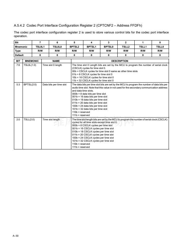
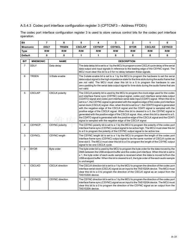
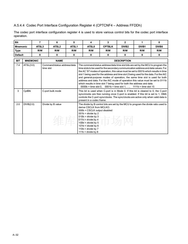
3. The MCU must also appropriately configure the C-port. (See Section 2.2.7.4 for more detail on initializing
the C-port). Note that if the C-port is placed in mode 0 (general-purpose mode) the CPTBLK bit in the codec
port interface configuration register 4 must be set to 1 to assure that SYNC is disabled when there is no valid
data in the buffer to be output.
4. Data is now ready to be received. The UBM, after receiving the bulk out packet and placing it in the
appropriate buffer, toggles the toggle bit if the double-buffer mode is set, sets the NACK bit to 1, stores the
packet data count in the data count register, and issues an interrupt to the MCU.
5. If the external device indicates that it is ready to receive data, the MCU enables the DMA process by setting
the DMAEN bit the DMA channel control register (DMACTL0 and DMACTL1). (Handshaking between the
MCU and external device will have to have taken place earlier to determine the status of the external
device).
6. Once enabled, the DMA engine proceeds to transfer the contents of the buffer(s) to the C-port for transmittal
to the external device. Data availability in the buffer(s) is determined by examining the NACK flags 鈥?which
are set to 1 when data has been received. For the double buffer case, the buffer to be used to retrieve data
for the C-port is determined by not only examining the NACK flags but also by monitoring the state of the
toggle bit. The NACK bit is cleared by the DMA logic (as opposed to the MCU) each time an entire buffer
content has been transferred to the C-port via DMA.
7. If the number of bulk out packets to be handled by the DMA process without MCU intervention is greater
than one (the number can be as high as 64K packets), multiple buffer writes take place before the DMA
process completes. Every time a data packet is written to a given buffer, the UBM generates the MCU
2鈥?9


 1
1
 2
2
 3
3
 4
4
 5
5
 6
6
 7
7
 8
8
 9
9
 10
10
 11
11
 12
12
 13
13
 14
14
 15
15
 16
16
 17
17
 18
18
 19
19
 20
20
 21
21
 22
22
 23
23
 24
24
 25
25
 26
26
 27
27
 28
28
 29
29
 30
30
 31
31
 32
32
 33
33
 34
34
 35
35
 36
36
 37
37
 38
38
 39
39
 40
40
 41
41
 42
42
 43
43
 44
44
 45
45
 46
46
 47
47
 48
48
 49
49
 50
50
 51
51
 52
52
 53
53
 54
54
 55
55
 56
56
 57
57
 58
58
 59
59
 60
60
 61
61
 62
62
 63
63
 64
64
 65
65
 66
66
 67
67
 68
68
 69
69
 70
70
 71
71
 72
72
 73
73
 74
74
 75
75
 76
76
 77
77
 78
78
 79
79
 80
80
 81
81
 82
82
 83
83
 84
84
 85
85
 86
86
 87
87
 88
88
 89
89
 90
90
 91
91
 92
92
 93
93
 94
94
 95
95
 96
96
 97
97
 98
98
 99
99
 100
100
 101
101
 102
102
 103
103
 104
104
 105
105
 106
106
 107
107
 108
108
 109
109
 110
110
 111
111
 112
112
 113
113
 114
114
