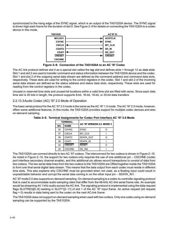
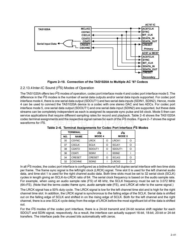
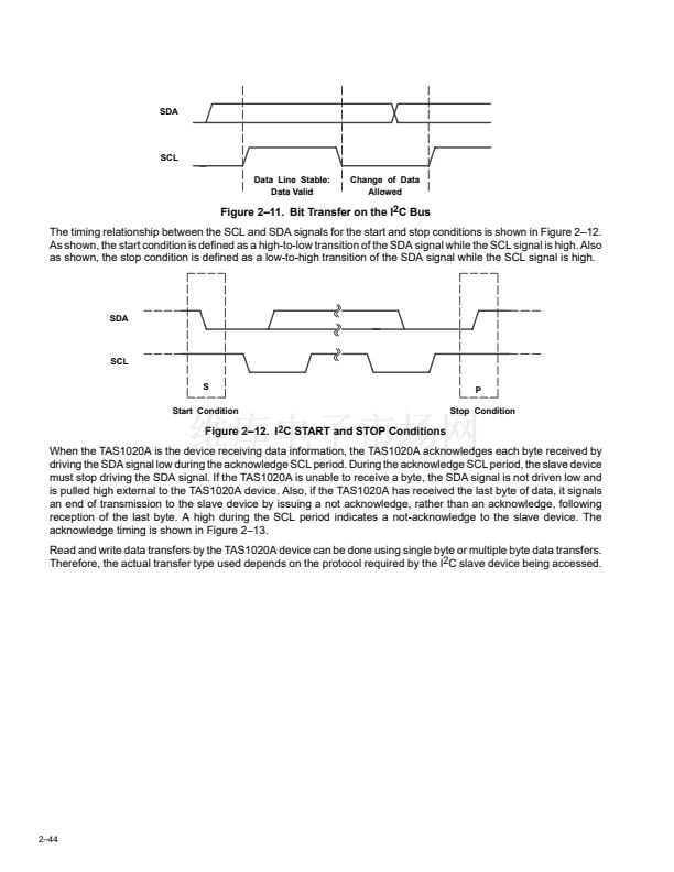
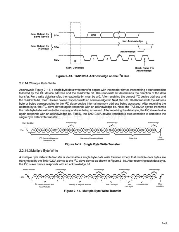
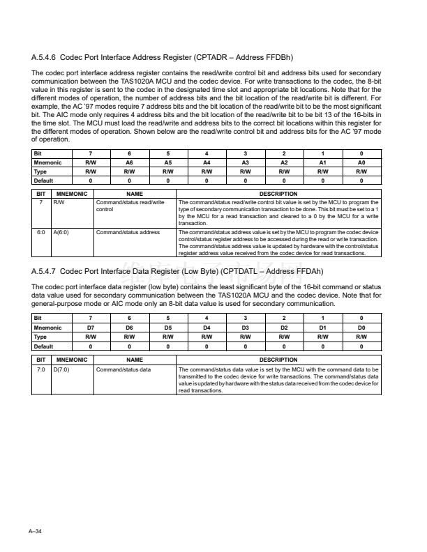
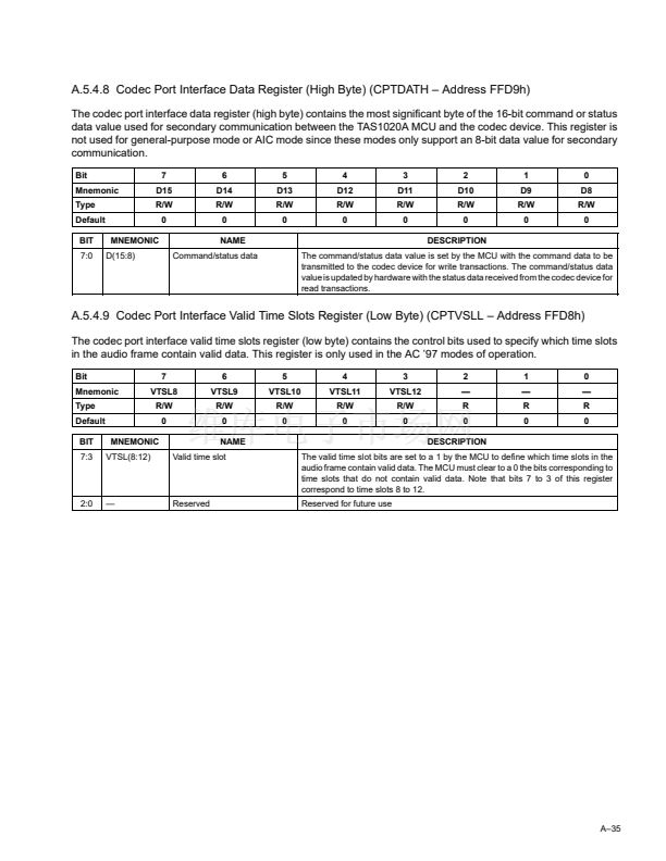
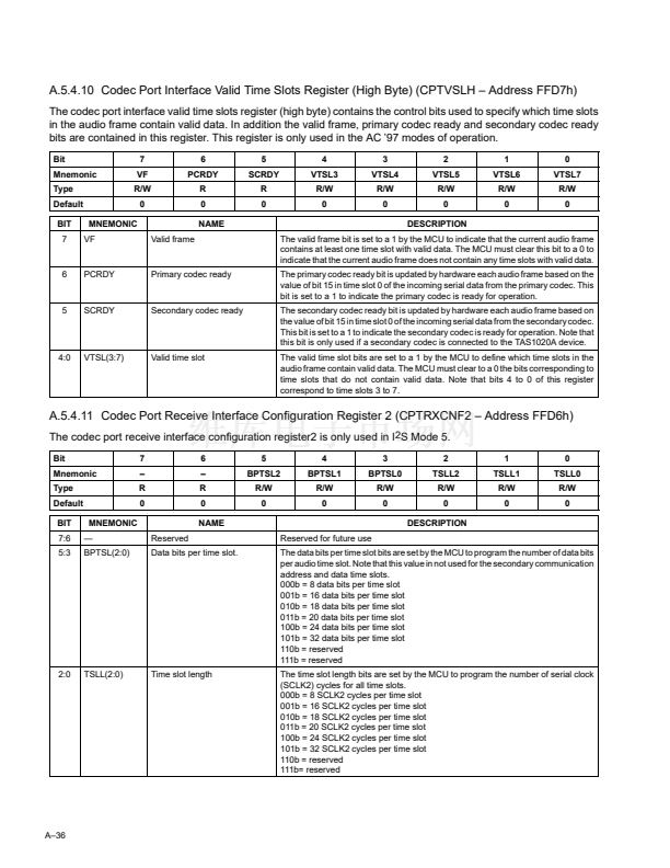
鈥?/div>
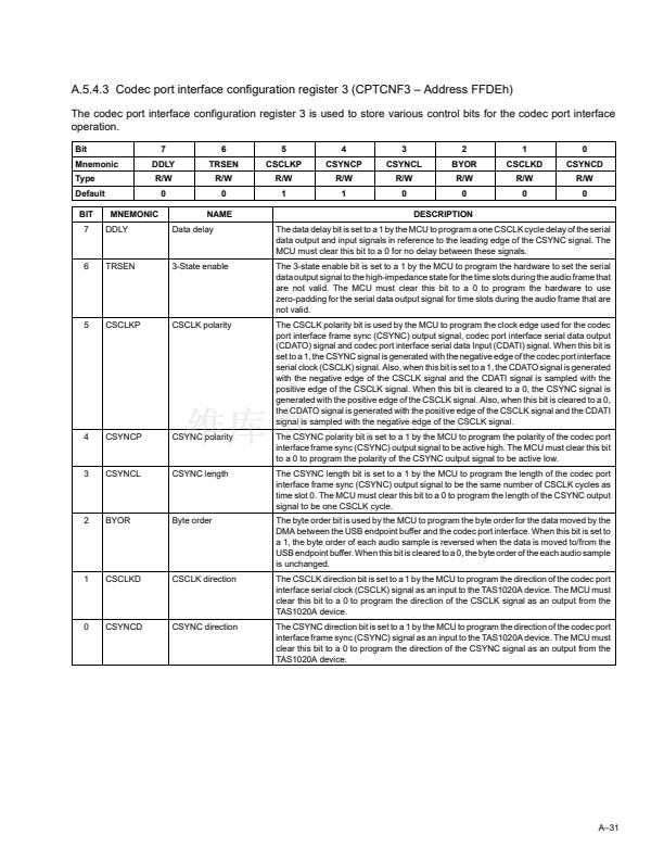
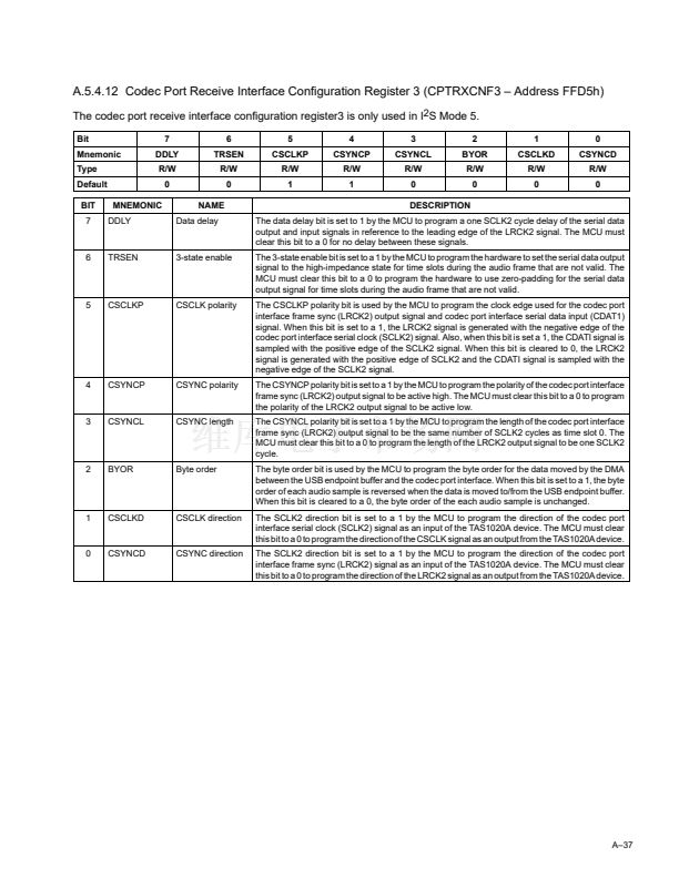
Setting the state of DDLY. A 1 programs a one CSCLK clock delay on the data output and data input
signals with reference to the leading edge of CSYNC. A 0 removes the delay.
Setting the state of TRSEN. A 1 sets the C-port output to the high-impedance state for those time
slots that have no valid data.
Setting the state of CSCLKP. A 1 programs the C-port to be CSCLK falling edge active (CDATO and
CSYNC transition on falling edge of CSCLK and DATI is sampled on rising edge of CSCLK). A 0
results in activity on the opposite edges of CSCLK.
Setting the state of CSYNCP. A 1 programs CSYNC to be active high. A 0 programs CSYNC to be
active low.
Setting the state of CSYNCL. A 1 programs the length of CSYNC to be the same number of CSCLK
cycles as time slot 0. A 0 programs CSYNC to be one CSCLK cycle in length.
Setting the state of BYOR. A 1 results in the DMA reversing the byte order in moving data to/from the
endpoint buffer.
Setting the state of CSCLKD. A 1 sets the CSCLK port as an input port (TAS1020A receives
CSCLK). A 0 sets the CSCLK port as an output port (TAS1020A sources CSCLK).
Setting the state of CSYNCD. A 1 sets the CSYNC port as an input port (TAS1020A receives
CSYNC). A 0 sets the CSYNC port as an output port (TAS1020A sources CSYNC).
3. The MCU configures the C-port. This entails:
鈥?/div>
鈥?/div>
鈥?/div>
鈥?/div>
鈥?/div>
鈥?/div>
鈥?/div>
鈥?/div>
鈥?/div>
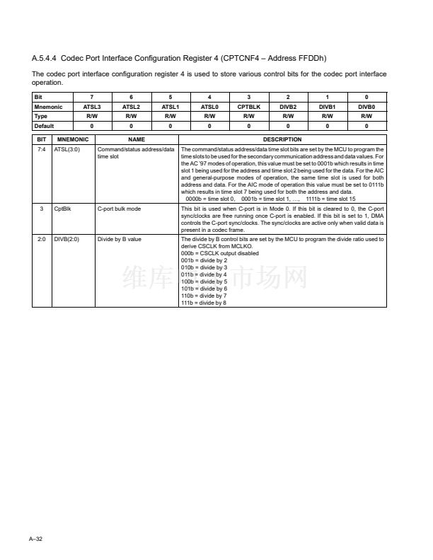
Programming register CPTCNF4, which consists of:
鈥?/div>
鈥?/div>
Specifying the 4-Bit field ATSL. This field defines which time slot is to be used for secondary
communication (command/status) address and data.
Setting the state of CPTBLK. When DMA is to be used to transport USB bulk transfers to external
devices via the C-port, the C-port must be placed in either a general-purpose mode or an AC97
mode, and CPTBLK must be set to one. When the C-port is placed in the general-purpose mode, a
state of 1 for CPTBLK results in CSYNC only being present when valid data is present in the current
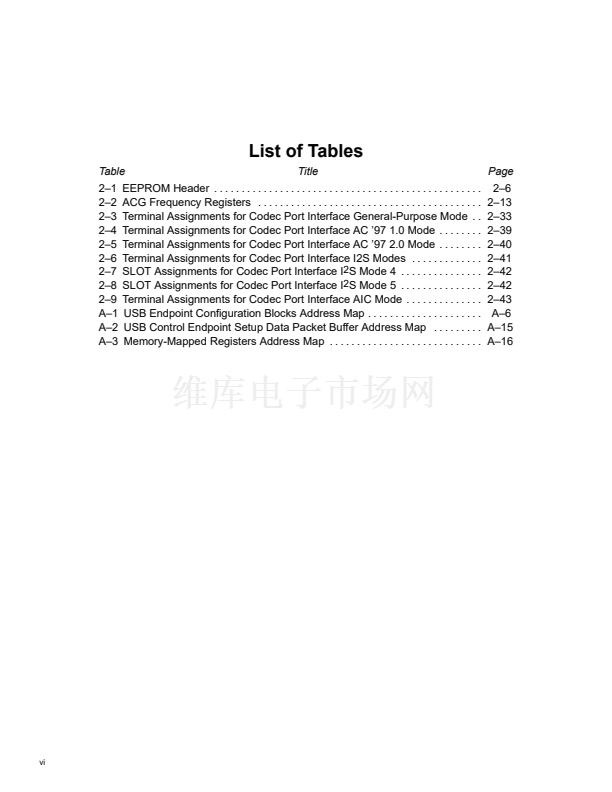
2鈥?1


 1
1
 2
2
 3
3
 4
4
 5
5
 6
6
 7
7
 8
8
 9
9
 10
10
 11
11
 12
12
 13
13
 14
14
 15
15
 16
16
 17
17
 18
18
 19
19
 20
20
 21
21
 22
22
 23
23
 24
24
 25
25
 26
26
 27
27
 28
28
 29
29
 30
30
 31
31
 32
32
 33
33
 34
34
 35
35
 36
36
 37
37
 38
38
 39
39
 40
40
 41
41
 42
42
 43
43
 44
44
 45
45
 46
46
 47
47
 48
48
 49
49
 50
50
 51
51
 52
52
 53
53
 54
54
 55
55
 56
56
 57
57
 58
58
 59
59
 60
60
 61
61
 62
62
 63
63
 64
64
 65
65
 66
66
 67
67
 68
68
 69
69
 70
70
 71
71
 72
72
 73
73
 74
74
 75
75
 76
76
 77
77
 78
78
 79
79
 80
80
 81
81
 82
82
 83
83
 84
84
 85
85
 86
86
 87
87
 88
88
 89
89
 90
90
 91
91
 92
92
 93
93
 94
94
 95
95
 96
96
 97
97
 98
98
 99
99
 100
100
 101
101
 102
102
 103
103
 104
104
 105
105
 106
106
 107
107
 108
108
 109
109
 110
110
 111
111
 112
112
 113
113
 114
114
