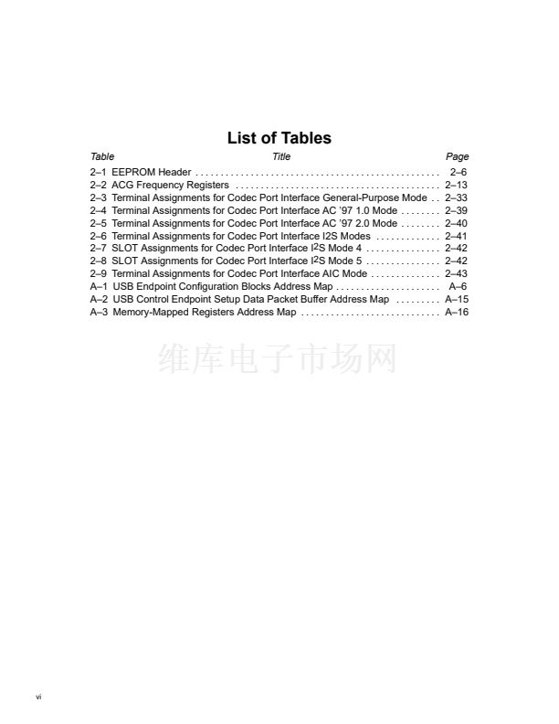
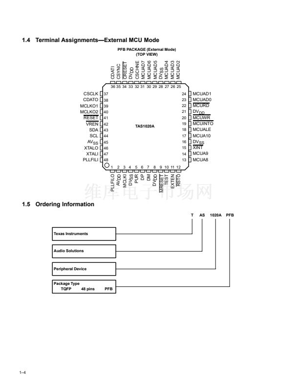
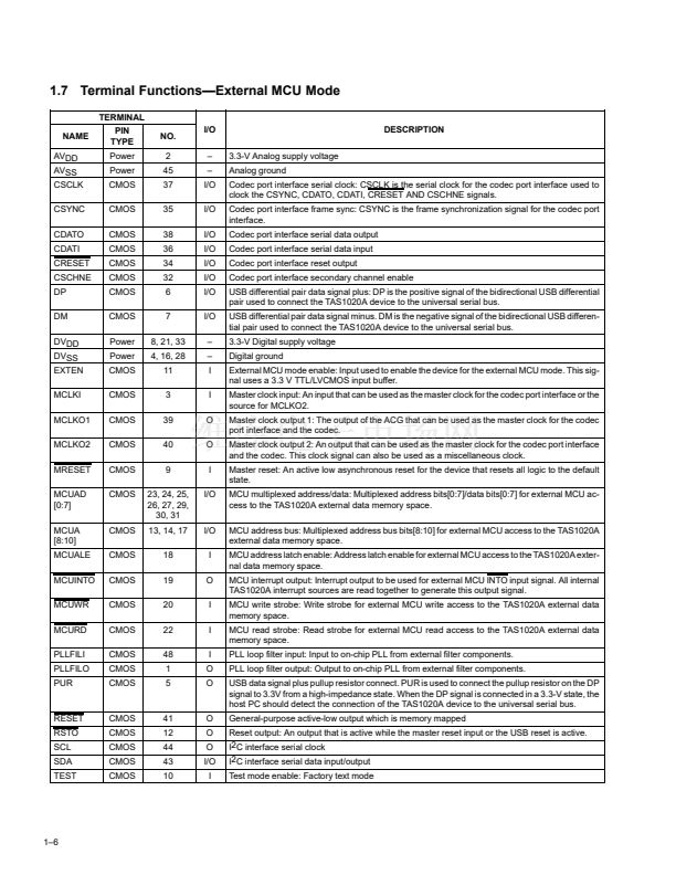
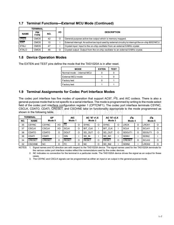
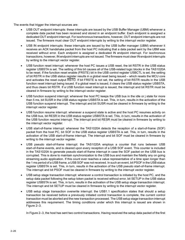
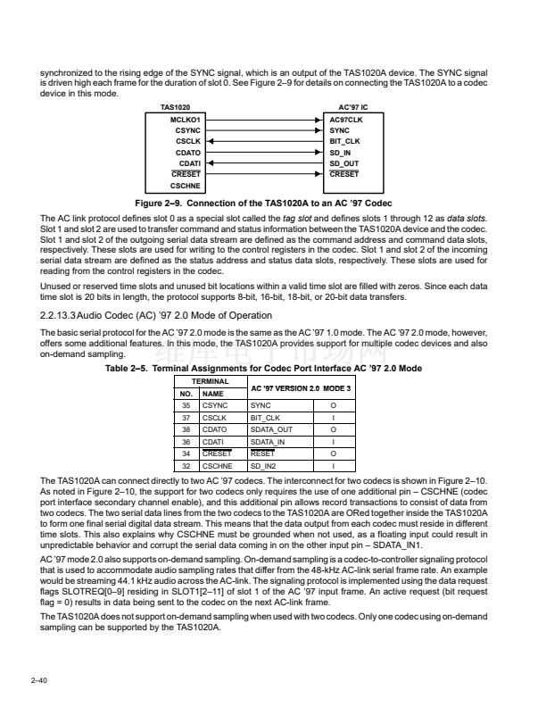
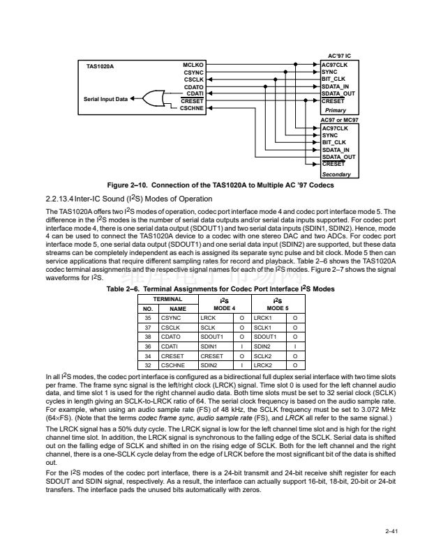
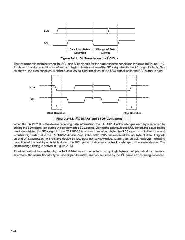
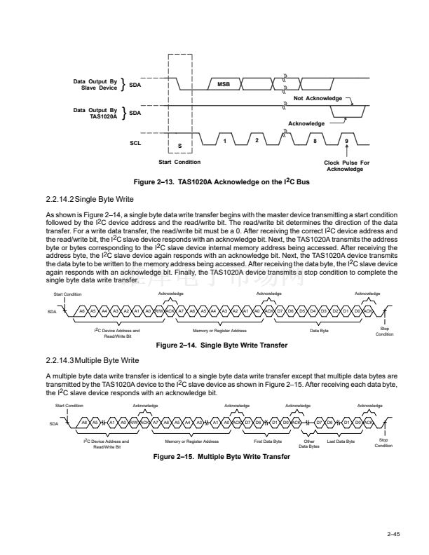
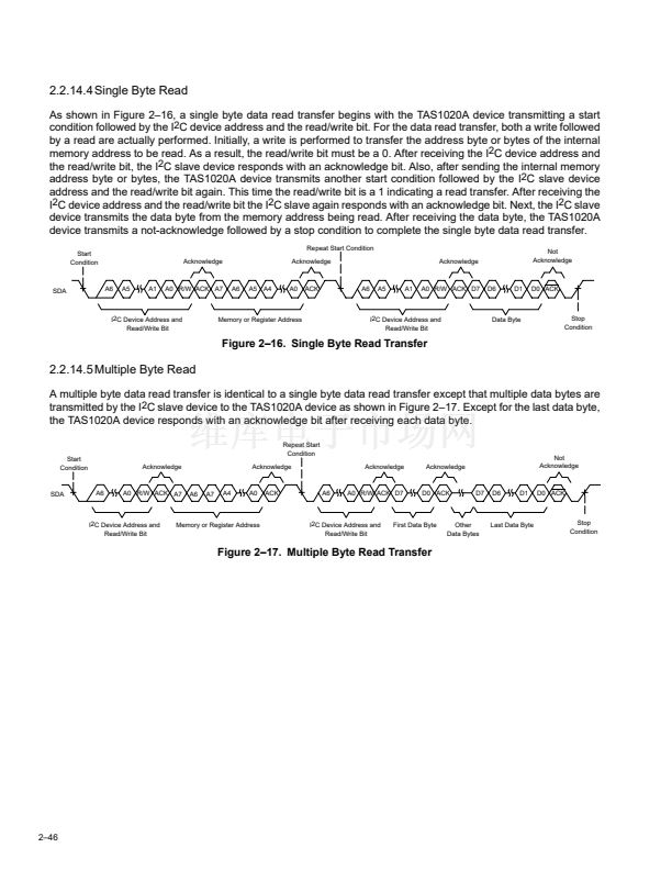
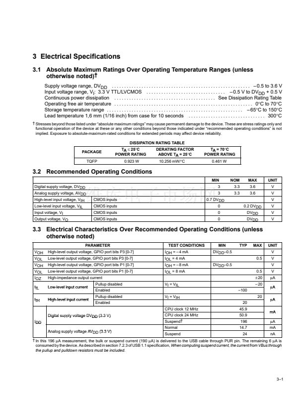
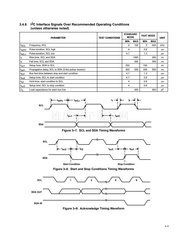
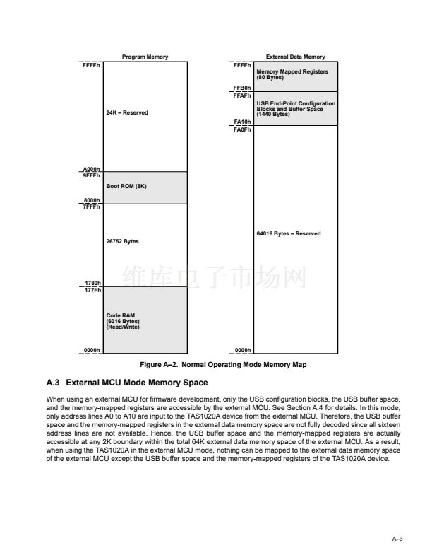
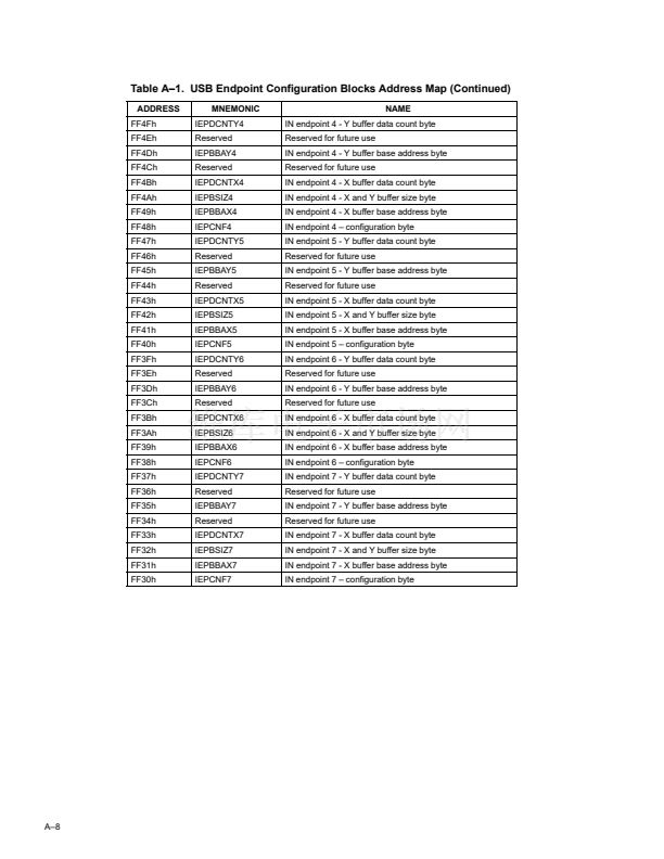
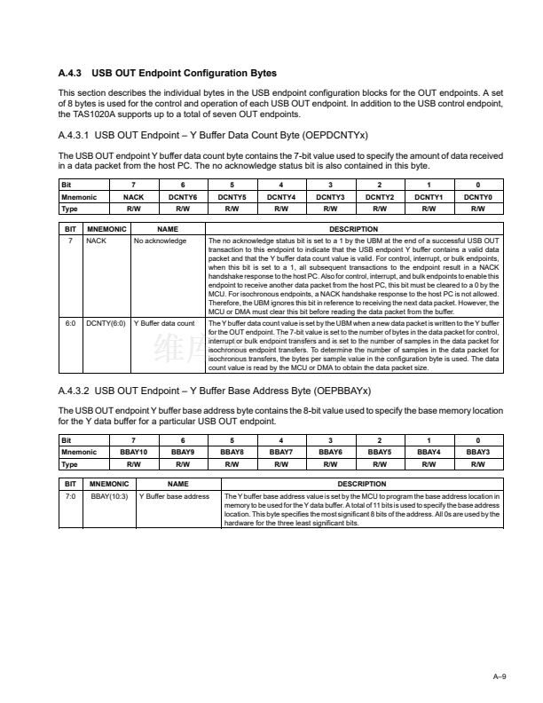
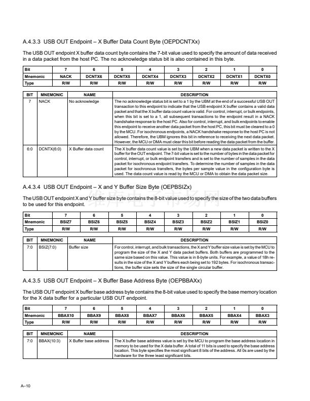
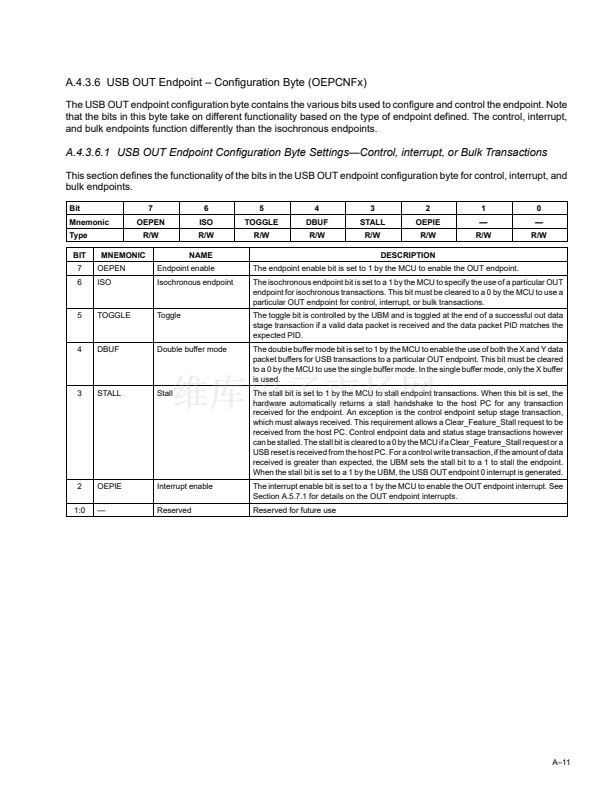
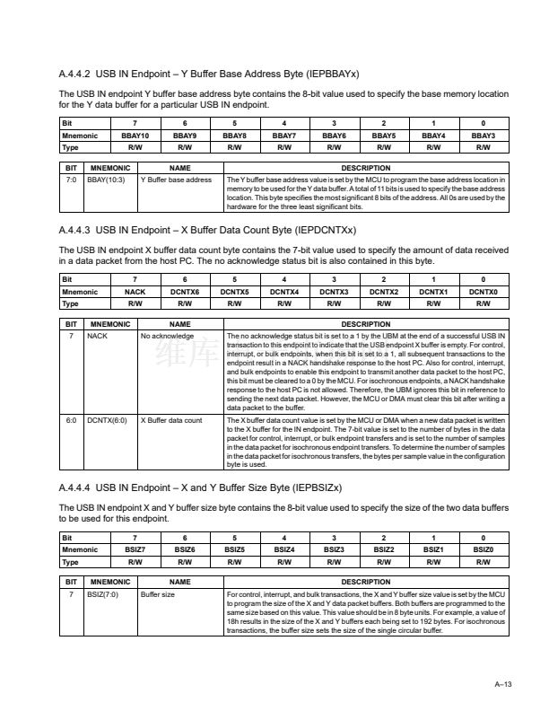
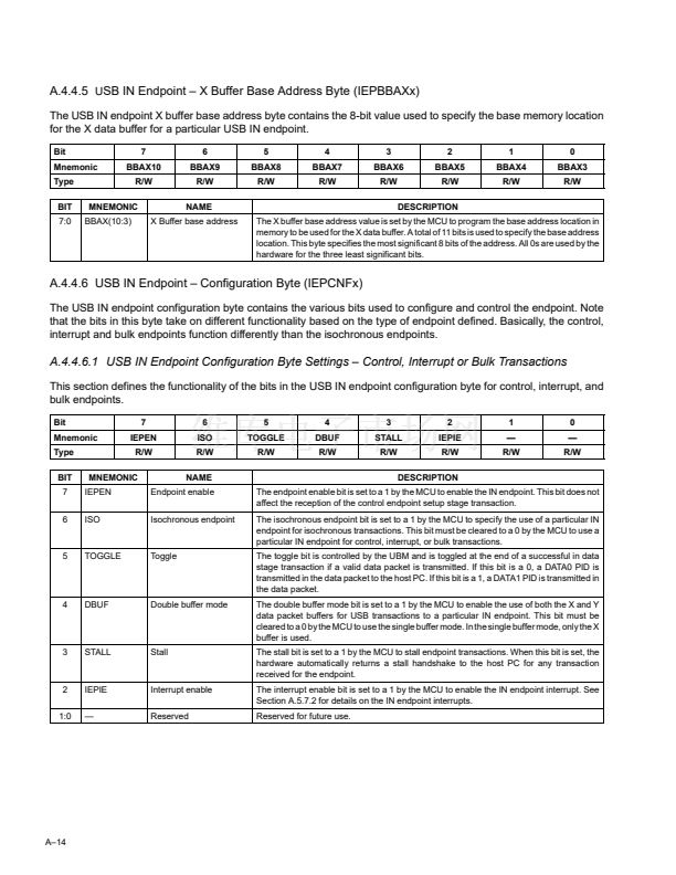
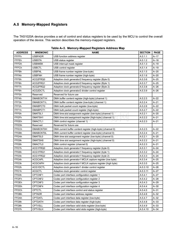
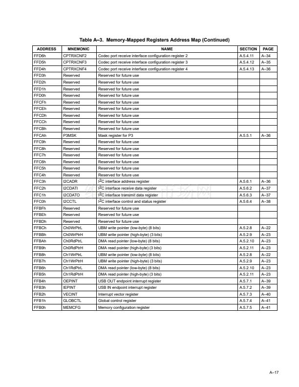
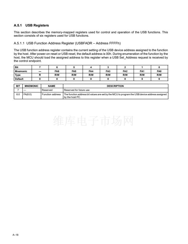
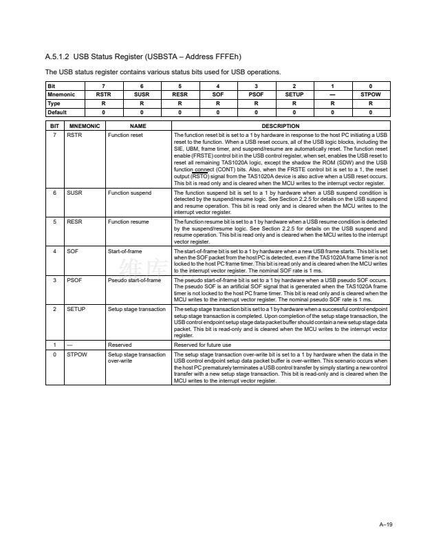
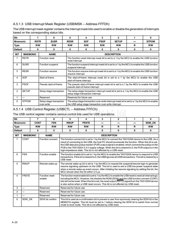
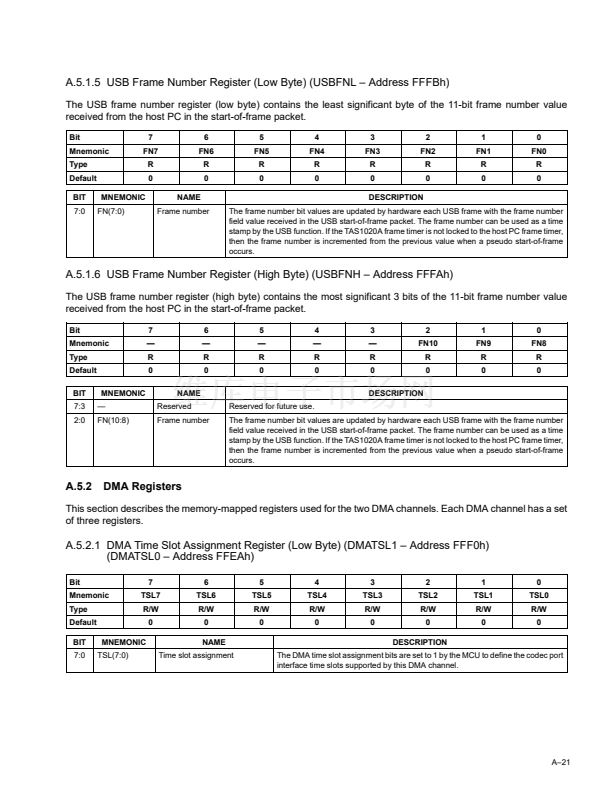
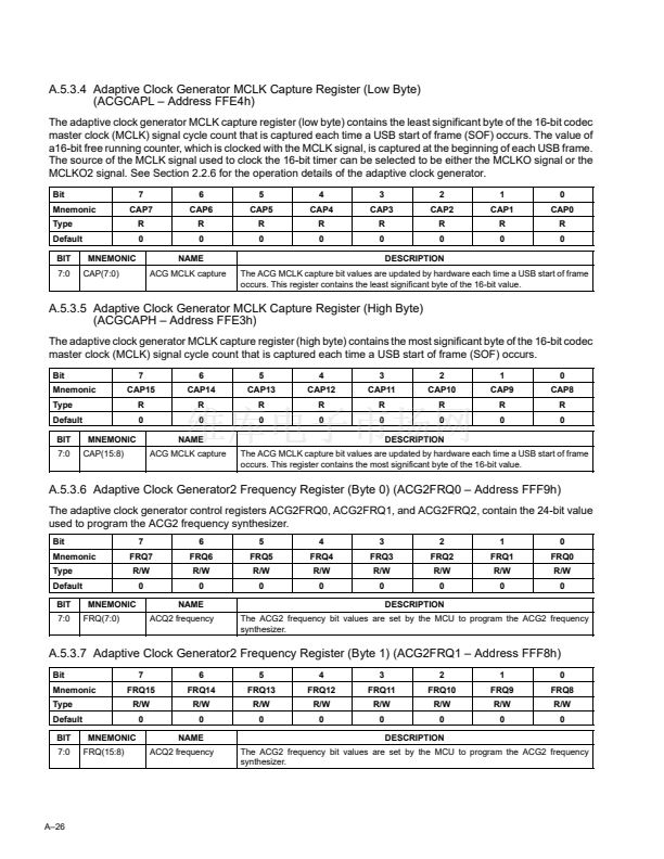
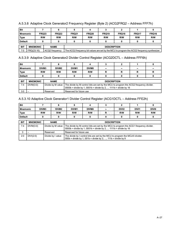
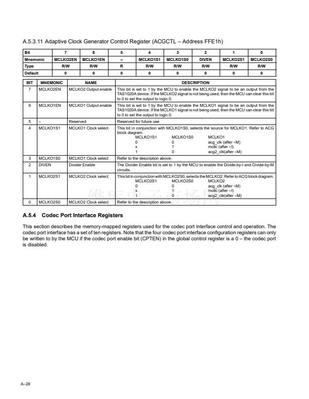
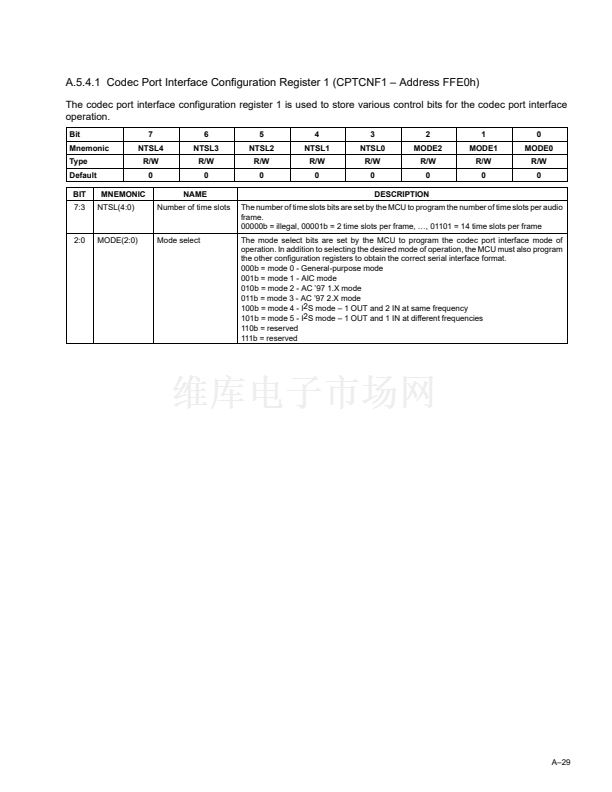
鈥?/div>
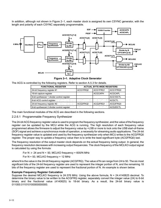
Specifying the 3-Bit field DIVB. This defines the divide ratio of MCLK to CSCLK.
Programming bits 4鈥? of register CPTCTL to enable or disable the C-port transmit and receive
interrupts. Bits 1鈥? of register CPTCTL are used to select between primary and secondary codecs
when using two codecs in the AC97 mode. Bit 0 of register CPTCTL (CRST), when cleared to 0, is used
to issue resets to external devices via the CRESET output pin.
NOTE:
C-port registers CPTADR, CPTDATL and CPTDATH are accessed during run time
operation to set the address, the data, and the mode (receive (status) or command (write)) for
secondary communications. Registers CPTVSLL and CPTVSLH are only used when the AC97
mode is selected and are used to specify which time slots in the audio frame contain valid data.
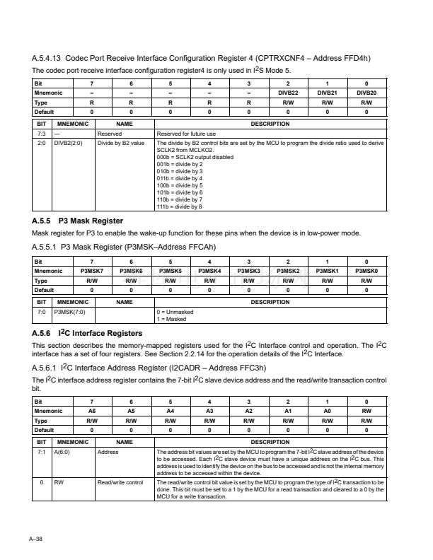
Registers CPTRXCNF2, CPTRXCNF3, and CPTRXCNF4 must be initialized when the C-port
is used in the I
2
S mode (mode 5) to support an ADC and a DAC running at different frequencies.
2.2.7.4.1 Circular Memory Buffer Implementation
A significant feature of DMA-supported isochronous transfers is the circular memory structure used to buffer the
incoming data. In most applications, the C-port timing is derived from the USB frame rate using a soft-PLL provided
in the TAS1020A firmware. However, the USB frame rate can vary within specified boundaries, and the output phase
of the PLL can lag (or lead) the input during such variations. If a linear ping pong buffer implementation is used,
tolerance must be built into switching between buffers to accommodate all possible magnitudes of variation in the
relative timing between the input and output time references. A circular buffer topology greatly simplifies the
implementation of the buffer as the need for decision points on when to switch buffers is eliminated.
The circular buffer implementation used in TAS1020A utilizes the same endpoint start (I/OEPBBAXx) and size
(I/OEPBSIZx) assignment used by the linear buffer implementation, and the size of the circular buffer is the size
specified in I/OEPBSIZx. The circular buffer implementation does require the use of two additional registers 鈥?a read
pointer and a write pointer. These two registers are controlled by hardware, but are made available to the MCU for
debug purposes.
Circular Buffer Operation for Isochronous OUT Transactions
The operation of the circular buffer for isochronous OUT transactions is as follows.
鈥?/div>
鈥?/div>
Initially, the
read
and
write
pointers are set in hardware to the OUT endpoint start address.
As the first packet of isochronous data addressed to the endpoint is received, the UBM stores the data into
the circular buffer and updates the value of the
write
pointer by a count of one for each byte written into the
buffer.
As soon as the DMA channel detects that the read and write pointers are not the same value (data is
available), the DMA channel could begin immediately retrieving data and outputting it to the C-port.
However, the DMA channel waits until the next USB SOF is received.
Once the DMA channel has waited until the next SOF is received, the buffer contains a full packet of data.
Upon receiving SOF, the DMA channel further waits until the start of the next C-port frame and then begins
transferring the buffered data to the C-port, updating the
read
pointer by one count for each byte of data
transferred. At the C-port the data is output to the external device in accordance with the timing
requirements of the external device (8 frames for 8 kHz audio sampling, 48 frames for 48 kHz audio
sampling, etc.). The DMA channel continues to retrieve data from the buffer and output it to the C-port,
update the
read
pointer, and check the value of the
write
pointer. Should the DMA-controlled
read
pointer
value ever equal the value of the UBM-controlled write pointer, the process goes on hold and awaits the
next USB SOF, where the process again resumes.
When the UBM completes writing a packet of data into the endpoint buffer, it loads the data count value of
that packer (number of data samples, not bytes) into field DCNTX/Y of register OEPDCNTX/Yx. The register
chosen, OEPDCNTX or OEPDCNTY, is determined by the LSB of the frame count register USBFNL. An


 1
1
 2
2
 3
3
 4
4
 5
5
 6
6
 7
7
 8
8
 9
9
 10
10
 11
11
 12
12
 13
13
 14
14
 15
15
 16
16
 17
17
 18
18
 19
19
 20
20
 21
21
 22
22
 23
23
 24
24
 25
25
 26
26
 27
27
 28
28
 29
29
 30
30
 31
31
 32
32
 33
33
 34
34
 35
35
 36
36
 37
37
 38
38
 39
39
 40
40
 41
41
 42
42
 43
43
 44
44
 45
45
 46
46
 47
47
 48
48
 49
49
 50
50
 51
51
 52
52
 53
53
 54
54
 55
55
 56
56
 57
57
 58
58
 59
59
 60
60
 61
61
 62
62
 63
63
 64
64
 65
65
 66
66
 67
67
 68
68
 69
69
 70
70
 71
71
 72
72
 73
73
 74
74
 75
75
 76
76
 77
77
 78
78
 79
79
 80
80
 81
81
 82
82
 83
83
 84
84
 85
85
 86
86
 87
87
 88
88
 89
89
 90
90
 91
91
 92
92
 93
93
 94
94
 95
95
 96
96
 97
97
 98
98
 99
99
 100
100
 101
101
 102
102
 103
103
 104
104
 105
105
 106
106
 107
107
 108
108
 109
109
 110
110
 111
111
 112
112
 113
113
 114
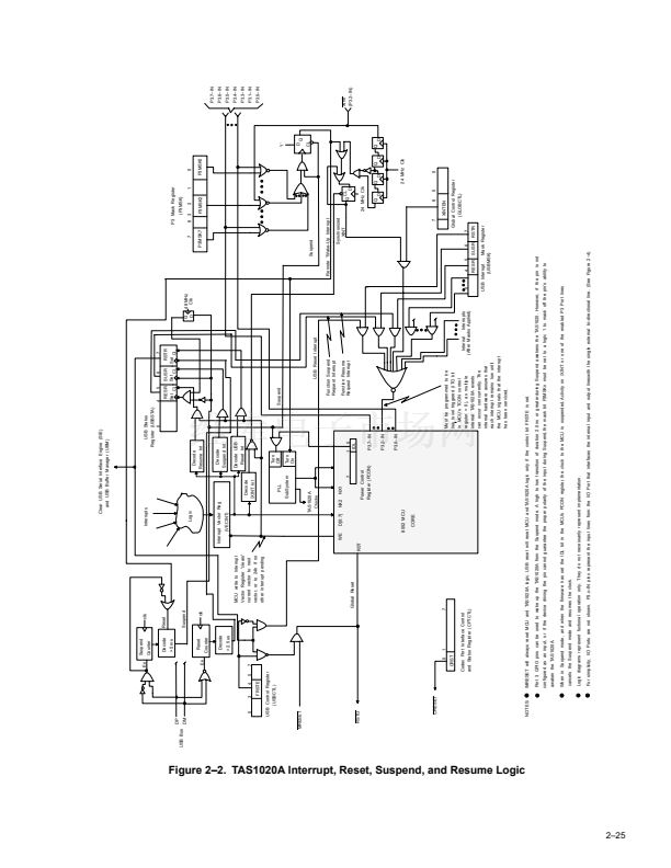
114
