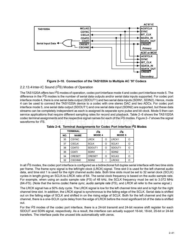
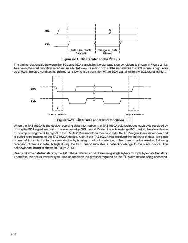
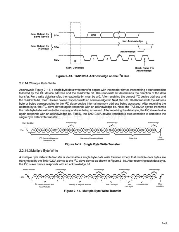
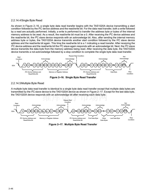
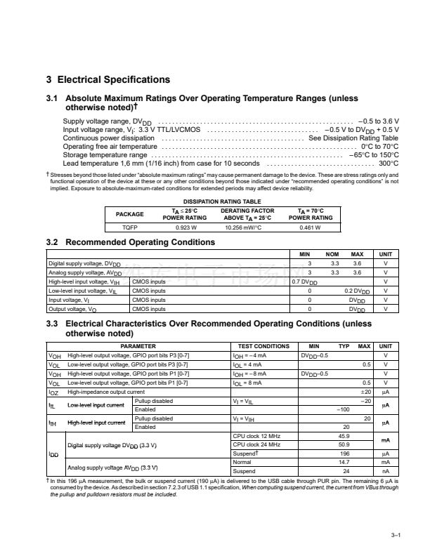
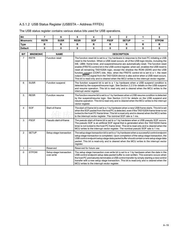
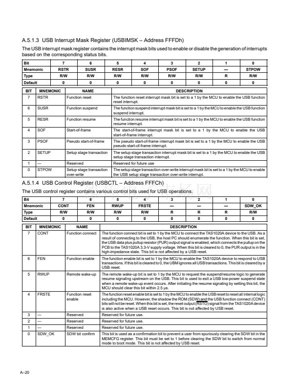
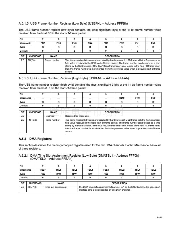
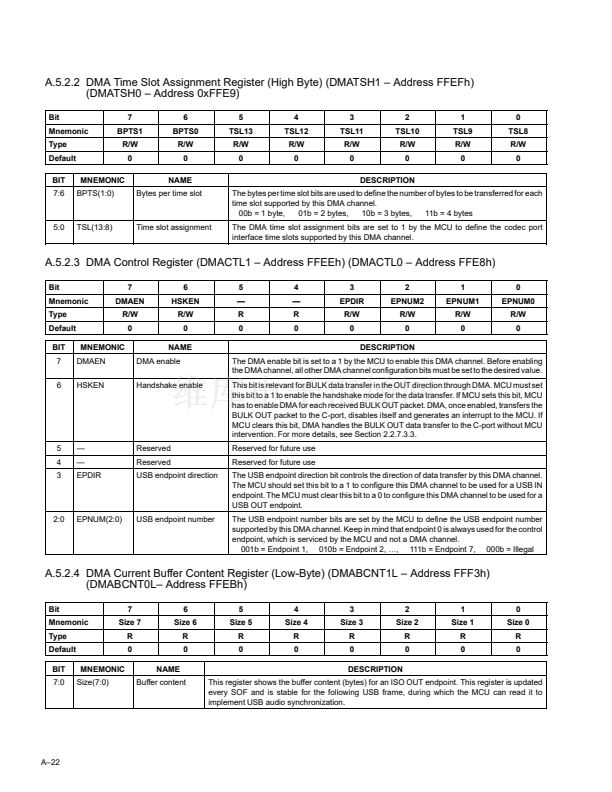
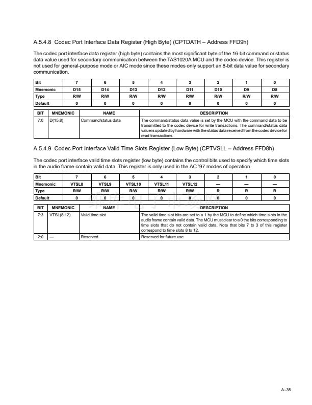
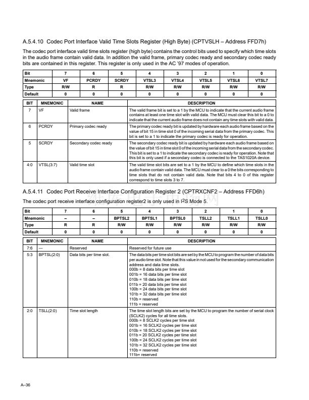
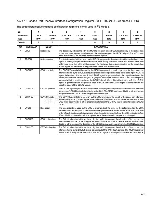
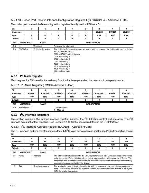
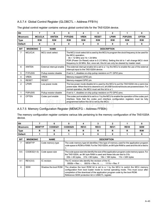
2.2.14.4 Single Byte Read
As shown in Figure 2鈥?6, a single byte data read transfer begins with the TAS1020A device transmitting a start
condition followed by the I
2
C device address and the read/write bit. For the data read transfer, both a write followed
by a read are actually performed. Initially, a write is performed to transfer the address byte or bytes of the internal
memory address to be read. As a result, the read/write bit must be a 0. After receiving the I
2
C device address and
the read/write bit, the I
2
C slave device responds with an acknowledge bit. Also, after sending the internal memory
address byte or bytes, the TAS1020A device transmits another start condition followed by the I
2
C slave device
address and the read/write bit again. This time the read/write bit is a 1 indicating a read transfer. After receiving the
I
2
C device address and the read/write bit the I
2
C slave again responds with an acknowledge bit. Next, the I
2
C slave
device transmits the data byte from the memory address being read. After receiving the data byte, the TAS1020A
device transmits a not-acknowledge followed by a stop condition to complete the single byte data read transfer.
Start
Condition
Repeat Start Condition
Acknowledge
Acknowledge
Acknowledge
Not
Acknowledge
SDA
A6
A5
A1
A0 R/W ACK A7
A6
A5
A4
A0
ACK
A6
A5
A1
A0 R/W ACK D7
D6
D1
D0 ACK
I2C Device Address and
Read/Write Bit
Memory or Register Address
I2C Device Address and
Read/Write Bit
Data Byte
Stop
Condition
Figure 2鈥?6. Single Byte Read Transfer
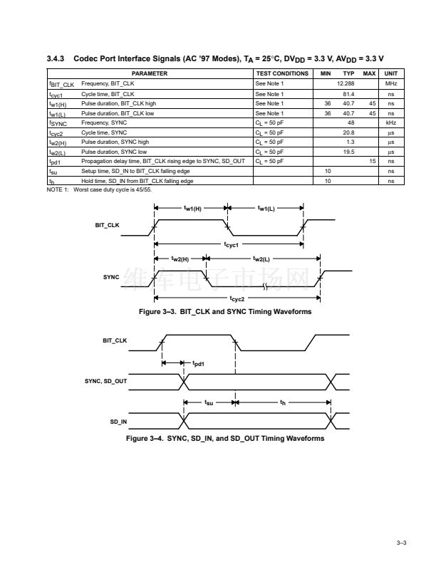
2.2.14.5 Multiple Byte Read
A multiple byte data read transfer is identical to a single byte data read transfer except that multiple data bytes are
transmitted by the I
2
C slave device to the TAS1020A device as shown in Figure 2鈥?7. Except for the last data byte,
the TAS1020A device responds with an acknowledge bit after receiving each data byte.
Repeat Start
Condition
Start
Condition
Acknowledge
Acknowledge
Acknowledge
Acknowledge
Not
Acknowledge
SDA
A6
A0 R/W ACK A7
A6
A7
A4
A0
ACK
A6
A0 R/W ACK D7
D0 ACK
D7
D6
D1
D0 ACK
I2C Device Address and
Read/Write Bit
Memory or Register Address
I2C Device Address and
Read/Write Bit
First Data Byte
Other
Data Bytes
Last Data Byte
Stop
Condition
Figure 2鈥?7. Multiple Byte Read Transfer
2鈥?6


 1
1
 2
2
 3
3
 4
4
 5
5
 6
6
 7
7
 8
8
 9
9
 10
10
 11
11
 12
12
 13
13
 14
14
 15
15
 16
16
 17
17
 18
18
 19
19
 20
20
 21
21
 22
22
 23
23
 24
24
 25
25
 26
26
 27
27
 28
28
 29
29
 30
30
 31
31
 32
32
 33
33
 34
34
 35
35
 36
36
 37
37
 38
38
 39
39
 40
40
 41
41
 42
42
 43
43
 44
44
 45
45
 46
46
 47
47
 48
48
 49
49
 50
50
 51
51
 52
52
 53
53
 54
54
 55
55
 56
56
 57
57
 58
58
 59
59
 60
60
 61
61
 62
62
 63
63
 64
64
 65
65
 66
66
 67
67
 68
68
 69
69
 70
70
 71
71
 72
72
 73
73
 74
74
 75
75
 76
76
 77
77
 78
78
 79
79
 80
80
 81
81
 82
82
 83
83
 84
84
 85
85
 86
86
 87
87
 88
88
 89
89
 90
90
 91
91
 92
92
 93
93
 94
94
 95
95
 96
96
 97
97
 98
98
 99
99
 100
100
 101
101
 102
102
 103
103
 104
104
 105
105
 106
106
 107
107
 108
108
 109
109
 110
110
 111
111
 112
112
 113
113
 114
114
