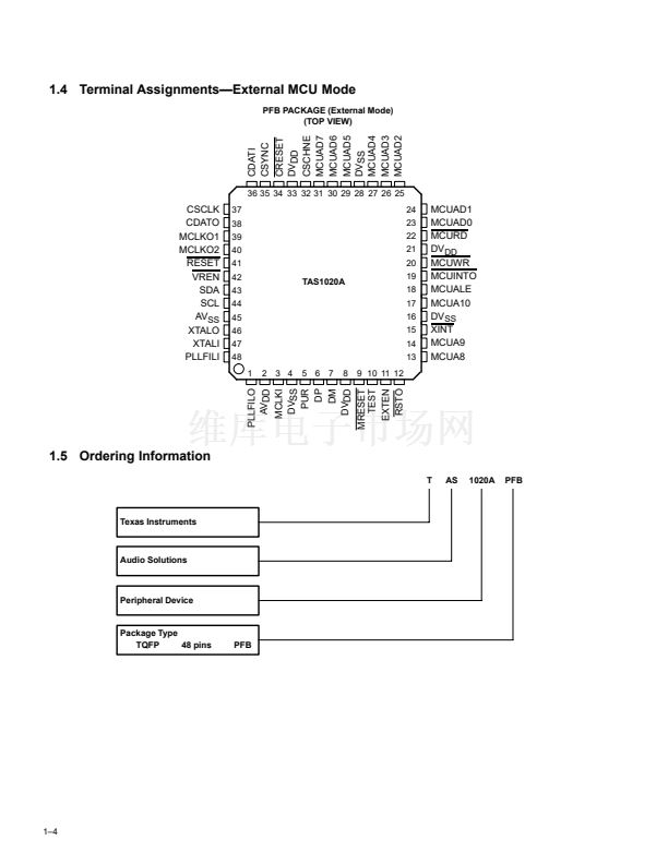
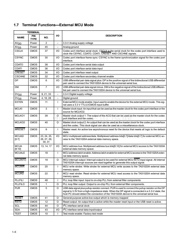
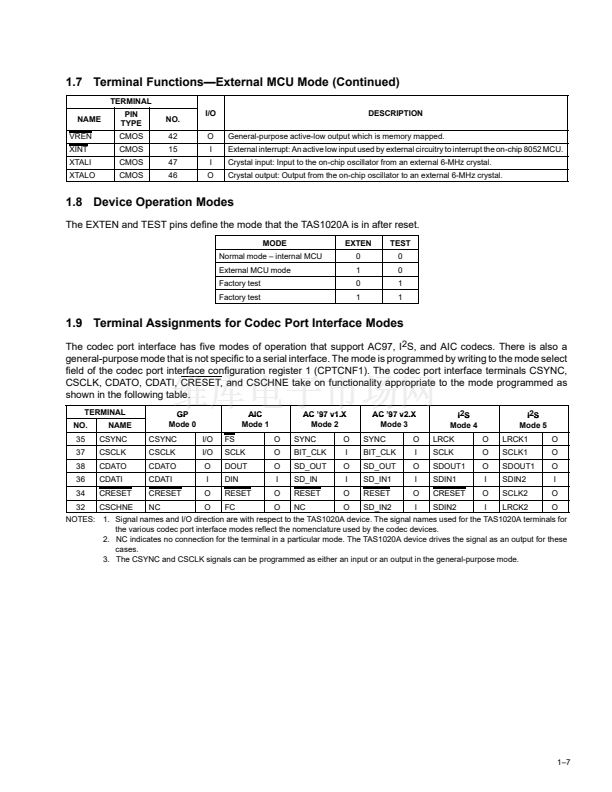
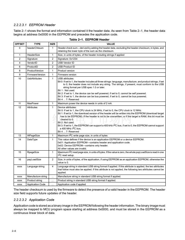
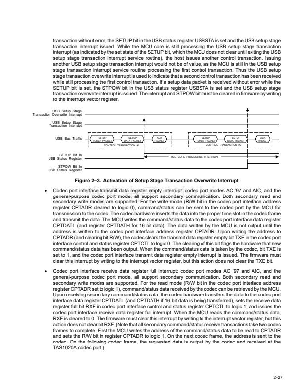
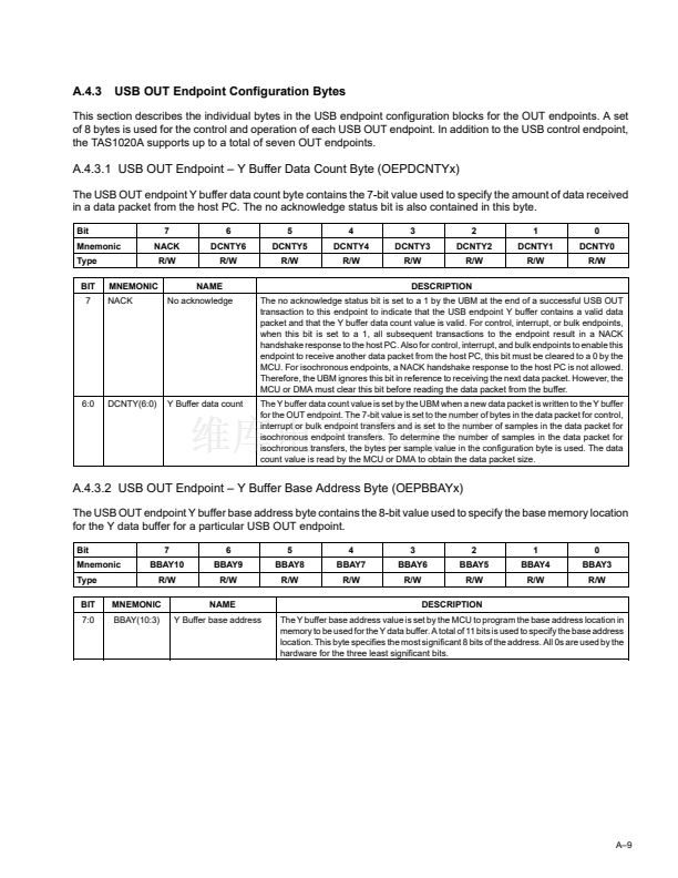
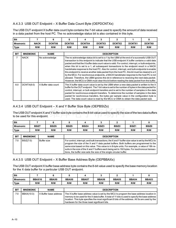
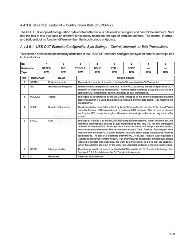
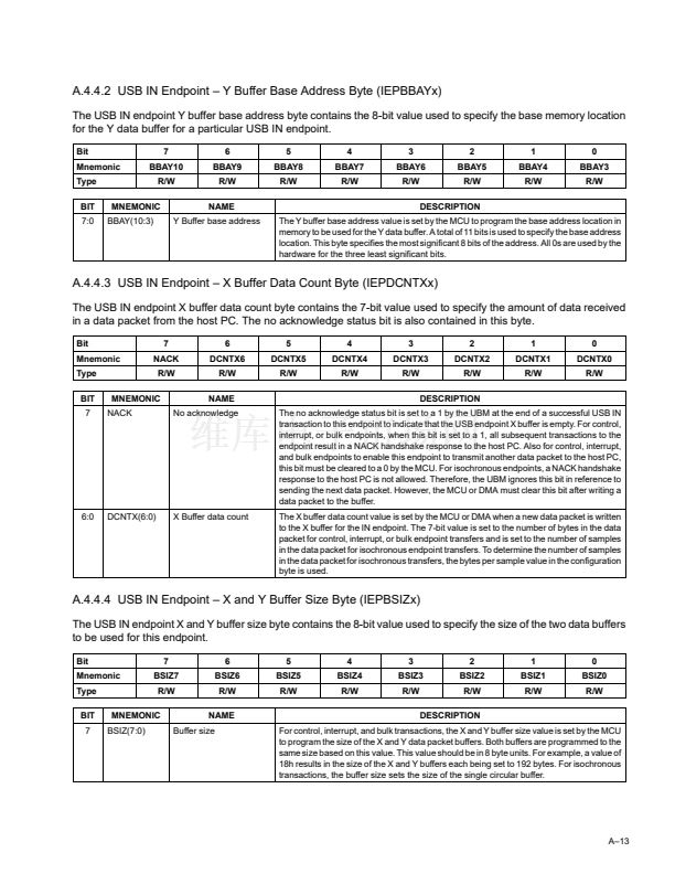
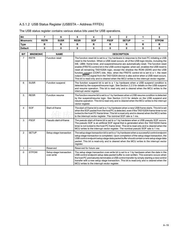
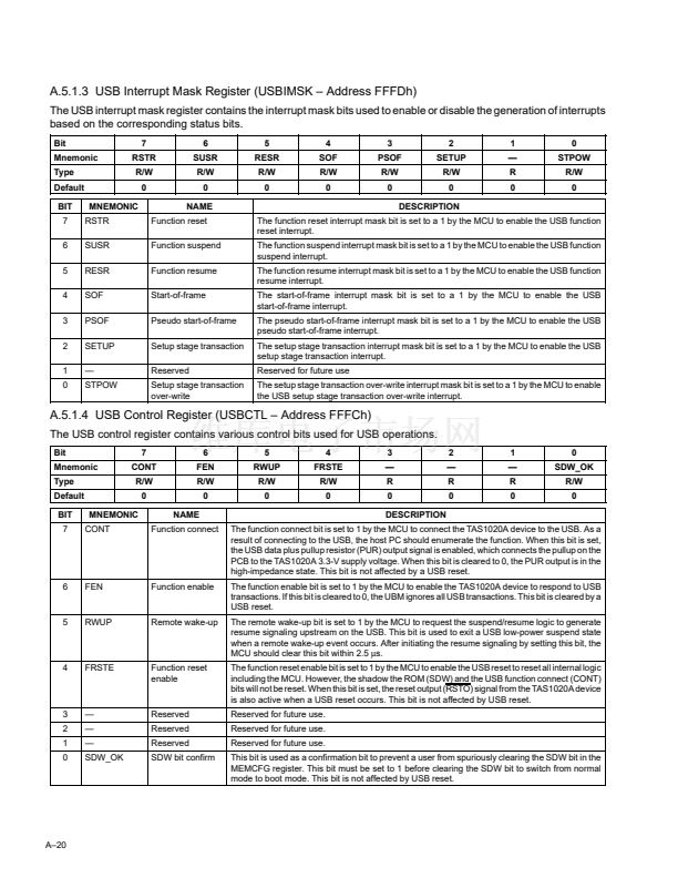
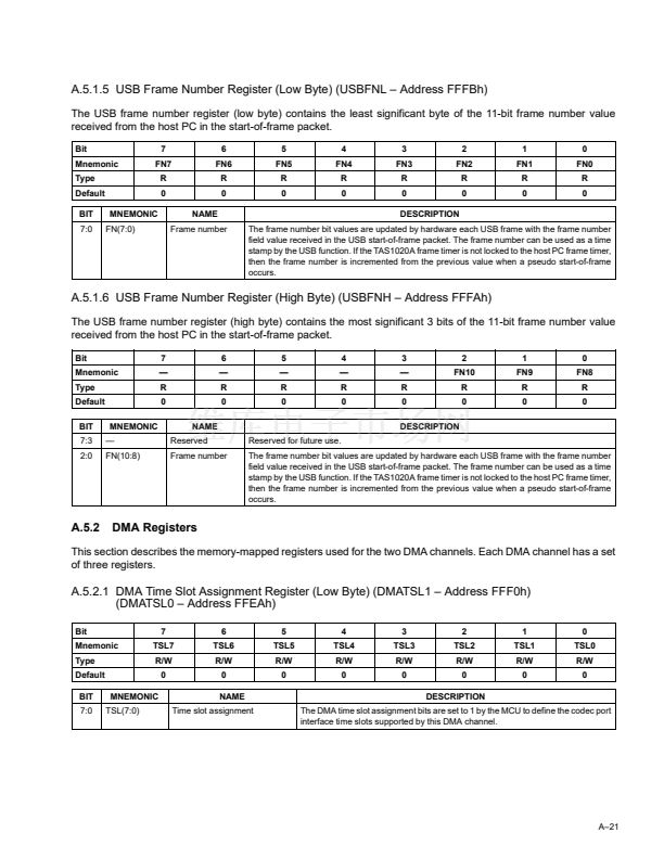
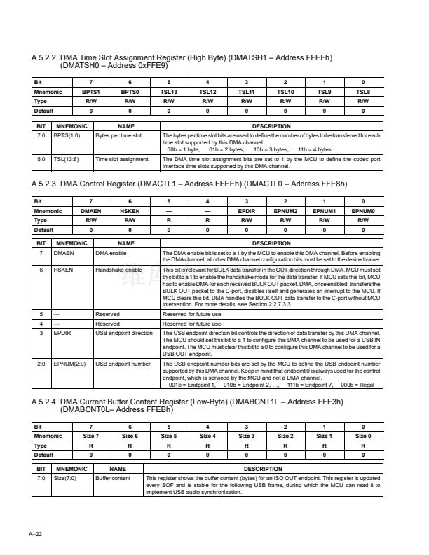
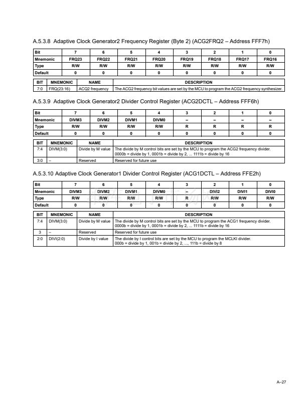
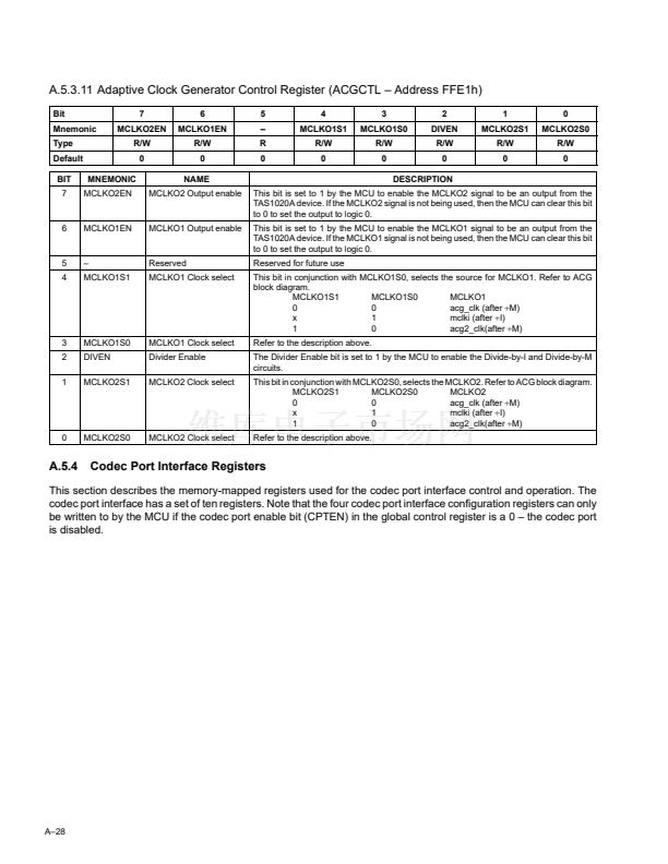
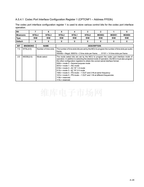
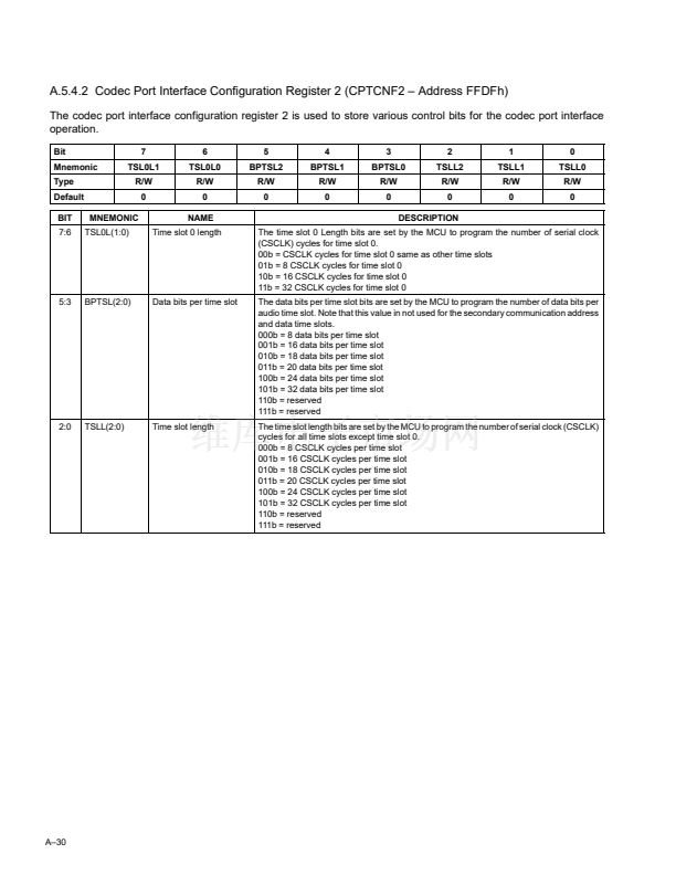
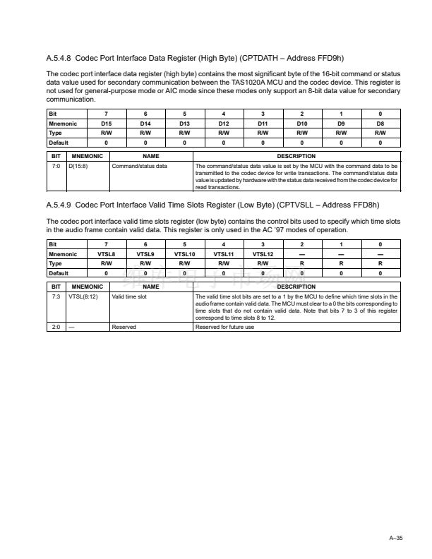
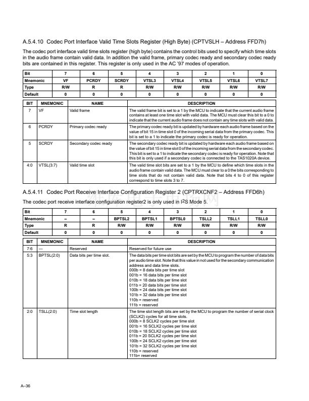
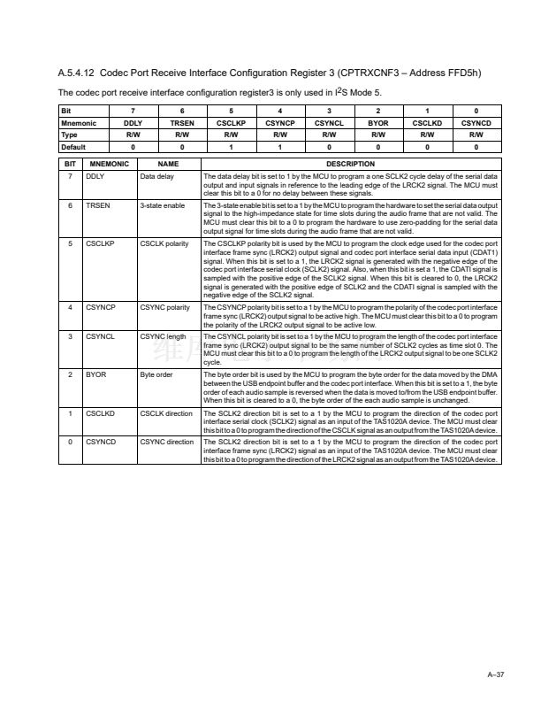
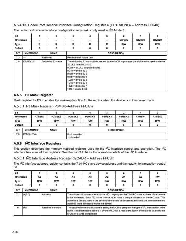
鈥?/div>
Supply voltage range, DV
DD
. . . . . . . . . . . . . . . . . . . . . . . . . . . . . . . . . . . . . . . . . . . . . . . . . . . . . . . . 鈥?0.5 to 3.6 V
Input voltage range, V
I
: 3.3 V TTL/LVCMOS . . . . . . . . . . . . . . . . . . . . . . . . . . . . . . . . 鈥?0.5 V to DV
DD
+ 0.5 V
Continuous power dissipation . . . . . . . . . . . . . . . . . . . . . . . . . . . . . . . . . . . . . . . . . See Dissipation Rating Table
Operating free air temperature . . . . . . . . . . . . . . . . . . . . . . . . . . . . . . . . . . . . . . . . . . . . . . . . . . . . . . . . 0掳C to 70掳C
Storage temperature range . . . . . . . . . . . . . . . . . . . . . . . . . . . . . . . . . . . . . . . . . . . . . . . . . . . . . . . 鈥?65掳C to 150掳C
Lead temperature 1,6 mm (1/16 inch) from case for 10 seconds . . . . . . . . . . . . . . . . . . . . . . . . . . . . . . . 300掳C
鈥?Stresses beyond those listed under 鈥渁bsolute maximum ratings鈥?may cause permanent damage to the device. These are stress ratings only and
functional operation of the device at these or any other conditions beyond those indicated under 鈥渞ecommended operating conditions鈥?is not
implied. Exposure to absolute-maximum-rated conditions for extended periods may affect device reliability.
DISSIPATION RATING TABLE
PACKAGE
TQFP
TA
鈮?/div>
25掳C
POWER RATING
0.923 W
DERATING FACTOR
ABOVE TA = 25掳C
10.256 mW/掳C
TA = 70掳C
POWER RATING
0.461 W
3.2 Recommended Operating Conditions
MIN
Digital supply voltage, DVDD
Analog supply voltage, AVDD
High-level input voltage, VIH
Low-level input voltage, VIL
Input voltage, VI
Output voltage, VO
CMOS inputs
CMOS inputs
CMOS inputs
CMOS inputs
3
3
0.7 DVDD
0
0
0
0.2 DVDD
DVDD
DVDD
NOM
3.3
3.3
MAX
3.6
3.6
UNIT
V
V
V
V
V
V
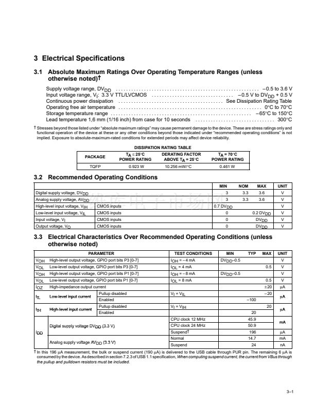
3.3 Electrical Characteristics Over Recommended Operating Conditions (unless
otherwise noted)
PARAMETER
VOH
VOL
VOH
VOL
IOZ
IIL
IIH
High-level output voltage, GPIO port bits P3 [0-7]
Low-level output voltage, GPIO port bits P3 [0-7]
High-level output voltage, GPIO port bits P1 [0-7]
Low-level output voltage, GPIO port bits P1 [0-7]
High-impedance output current
Low level input current
Low-level
High-level
High level input current
Pullup disabled
Enabled
Pullup disabled
Enabled
CPU clock 12 MHz
Digital su ly voltage DVDD (3.3 V)
supply
IDD
Analog supply voltage AVDD (3 3 V)
(3.3
CPU clock 24 MHz
Suspend鈥?/div>
Normal
Suspend
VI = VIH
20
45.9
50.9
196
14.7
24
VI = VIL
鈥?00
20
TEST CONDITIONS
IOH = 鈥?4 mA
IOL = 4 mA
IOH = 鈥?8 mA
IOL = 8 mA
MIN
DVDD鈥?.5
0.5
DVDD鈥?.5
0.5
卤
20
鈥?20
TYP
MAX
UNIT
V
V
V
V
碌A
碌A
碌A
mA
碌A
mA
nA
鈥?In this 196
碌A
measurement, the bulk or suspend current (190
碌A)
is delivered to the USB cable through PUR pin. The remaining 6
碌A
is
consumed by the device. As described in section 7.2.3 of USB 1.1 specification,
When computing suspend current, the current from VBus through
the pullup and pulldown resistors must be included.
3鈥?


 1
1
 2
2
 3
3
 4
4
 5
5
 6
6
 7
7
 8
8
 9
9
 10
10
 11
11
 12
12
 13
13
 14
14
 15
15
 16
16
 17
17
 18
18
 19
19
 20
20
 21
21
 22
22
 23
23
 24
24
 25
25
 26
26
 27
27
 28
28
 29
29
 30
30
 31
31
 32
32
 33
33
 34
34
 35
35
 36
36
 37
37
 38
38
 39
39
 40
40
 41
41
 42
42
 43
43
 44
44
 45
45
 46
46
 47
47
 48
48
 49
49
 50
50
 51
51
 52
52
 53
53
 54
54
 55
55
 56
56
 57
57
 58
58
 59
59
 60
60
 61
61
 62
62
 63
63
 64
64
 65
65
 66
66
 67
67
 68
68
 69
69
 70
70
 71
71
 72
72
 73
73
 74
74
 75
75
 76
76
 77
77
 78
78
 79
79
 80
80
 81
81
 82
82
 83
83
 84
84
 85
85
 86
86
 87
87
 88
88
 89
89
 90
90
 91
91
 92
92
 93
93
 94
94
 95
95
 96
96
 97
97
 98
98
 99
99
 100
100
 101
101
 102
102
 103
103
 104
104
 105
105
 106
106
 107
107
 108
108
 109
109
 110
110
 111
111
 112
112
 113
113
 114
114
