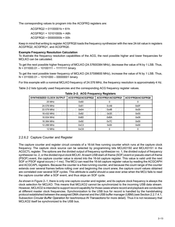
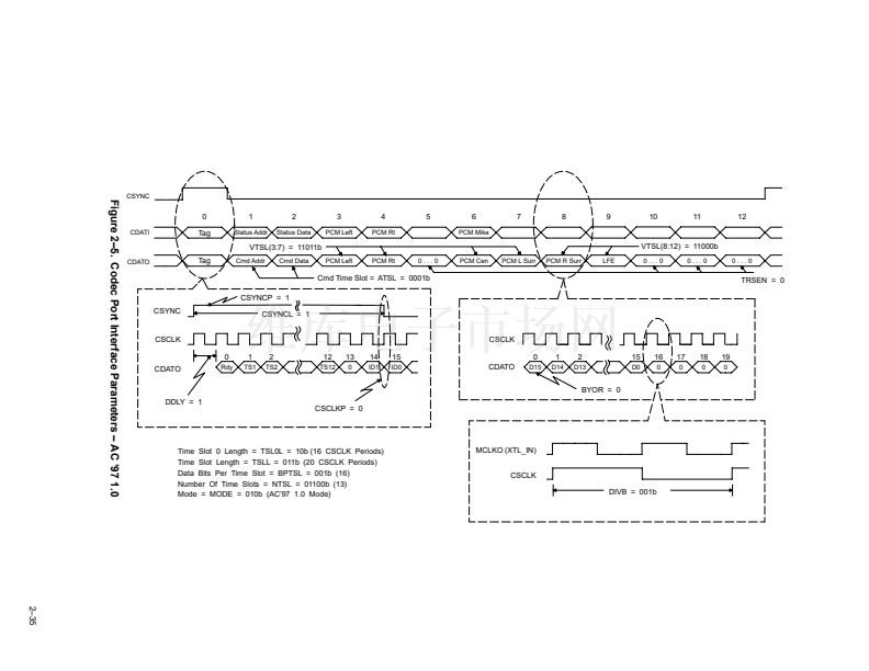
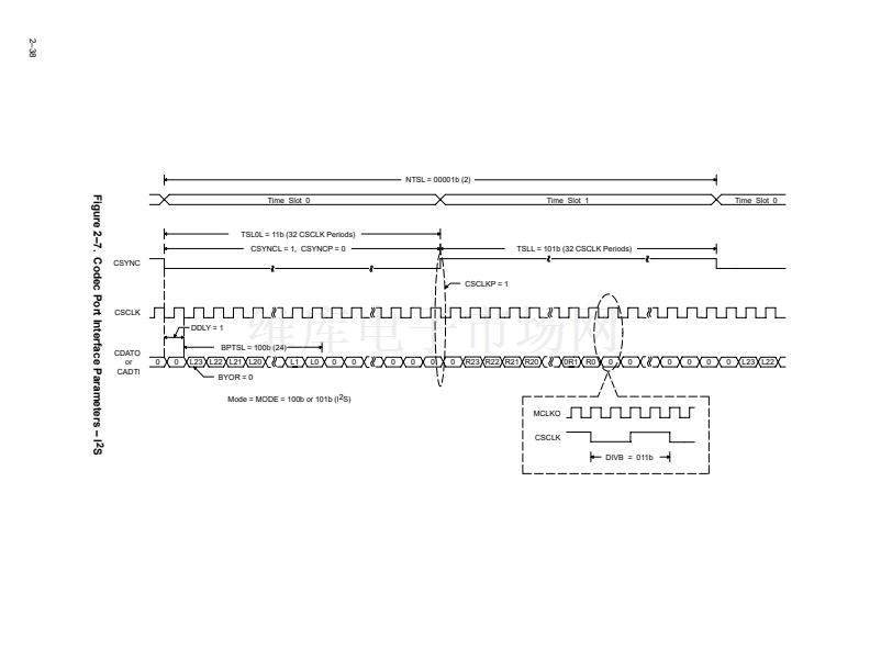
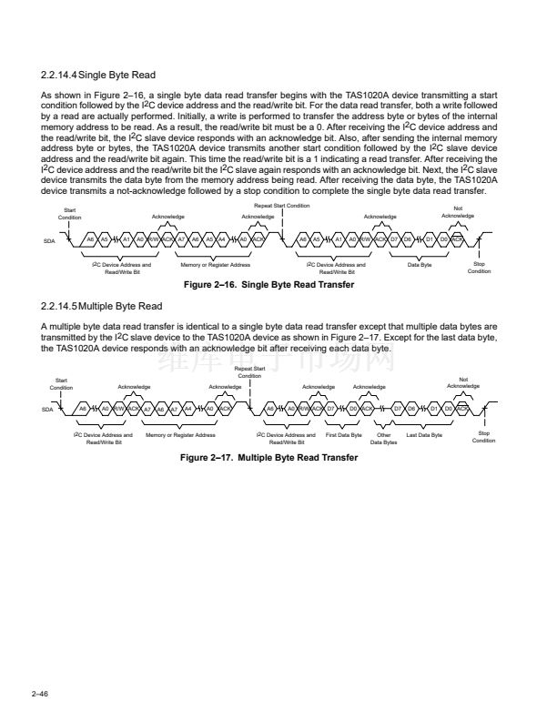
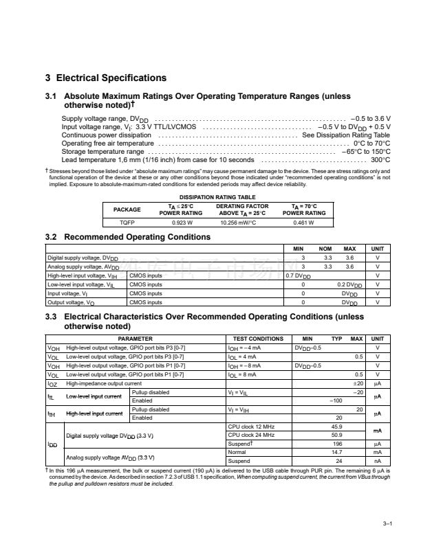
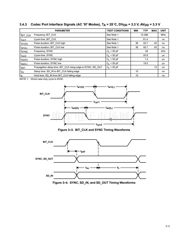
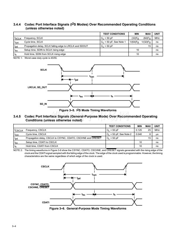
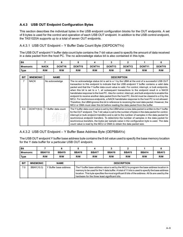
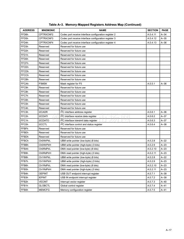
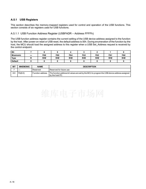
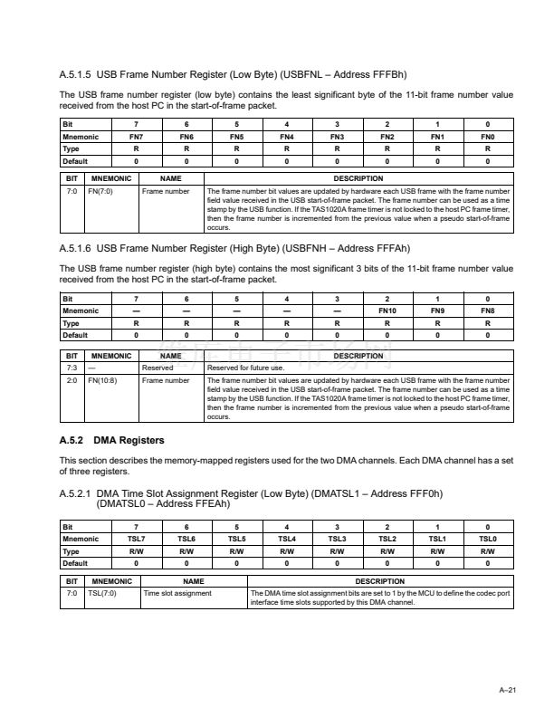
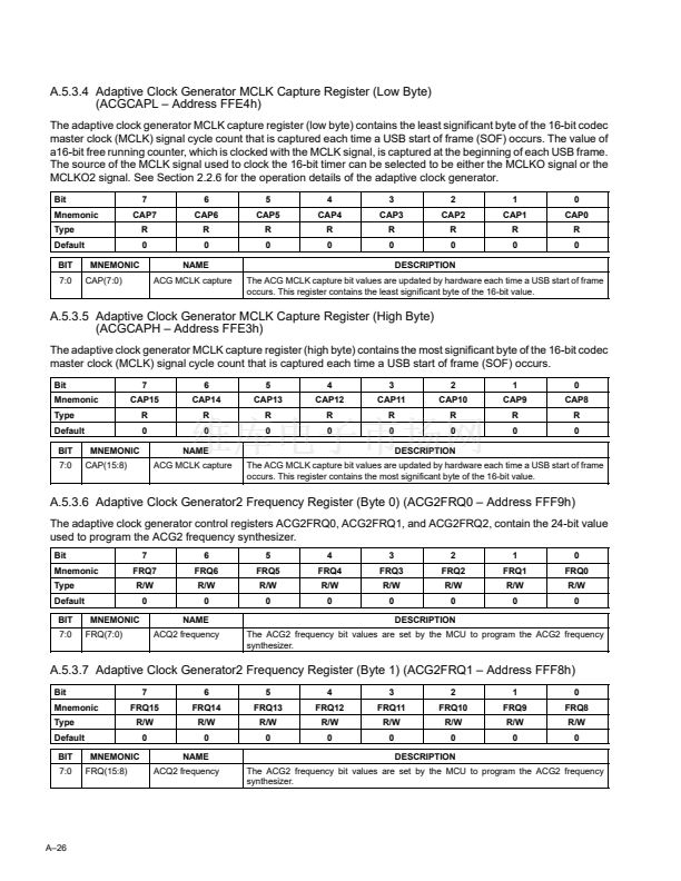
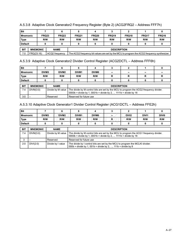
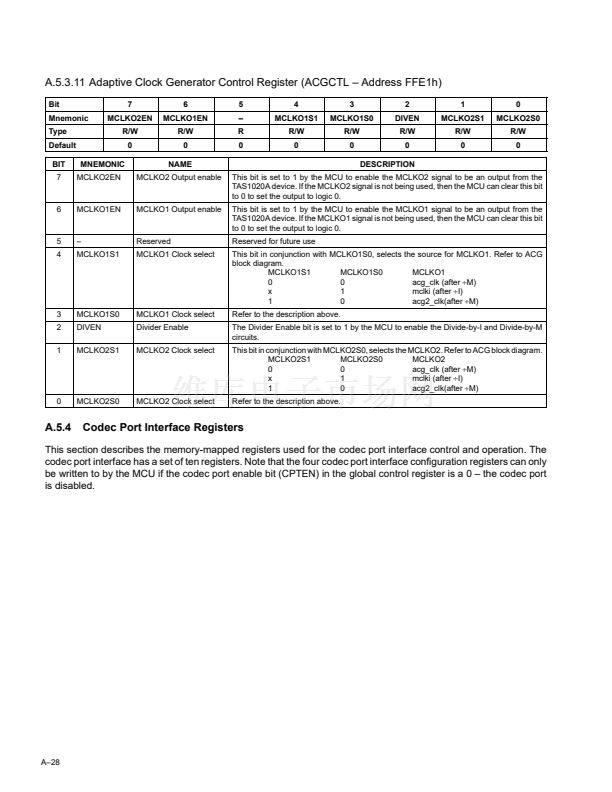
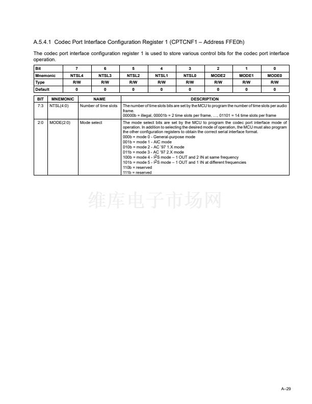
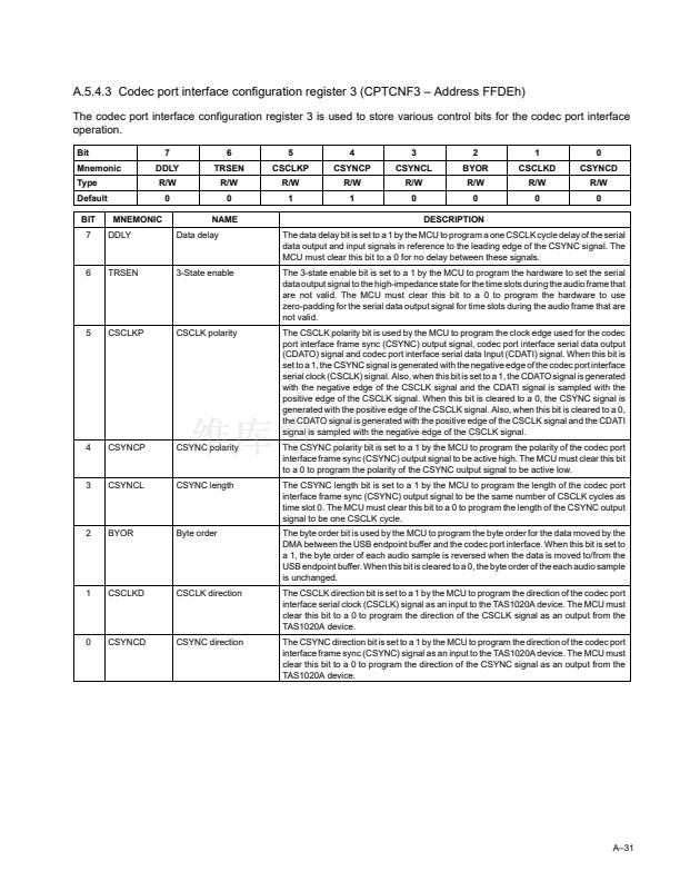
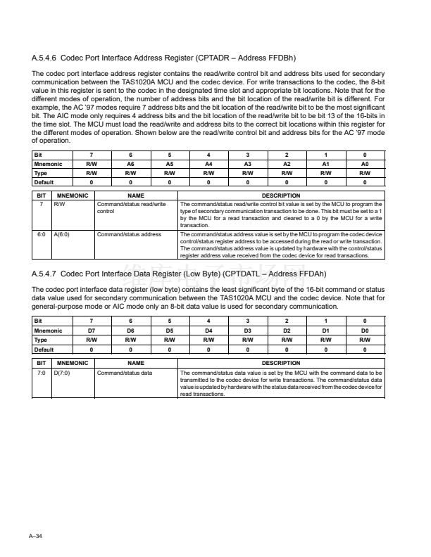
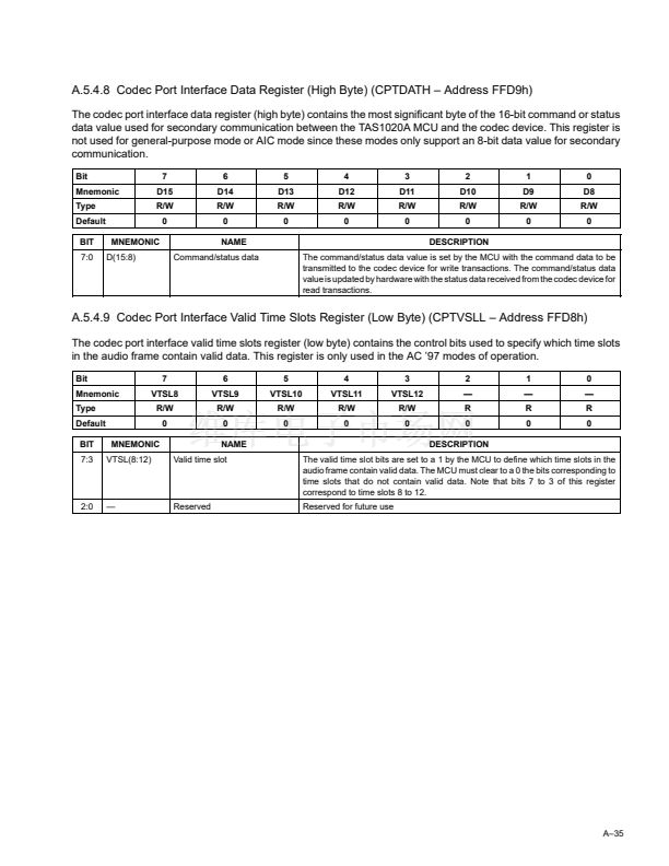
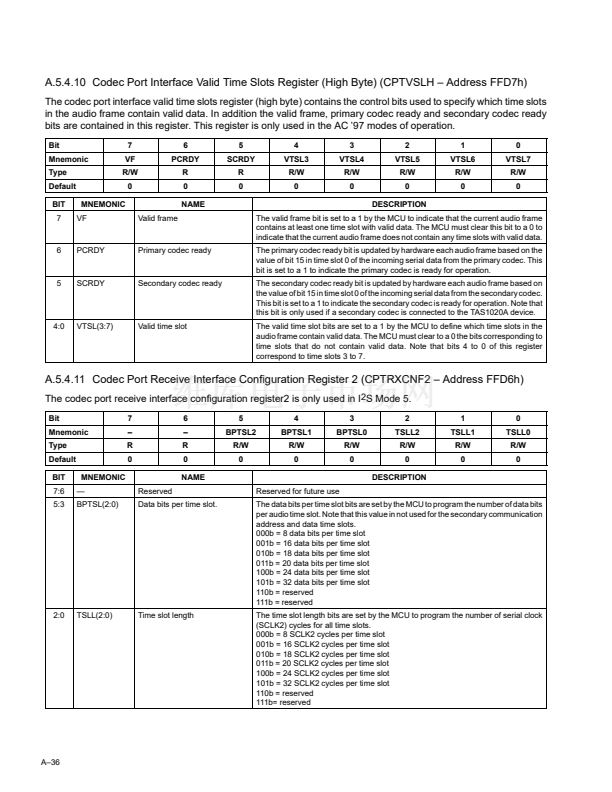
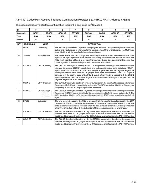
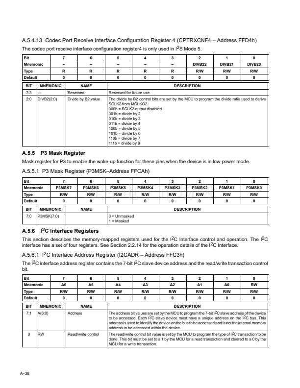
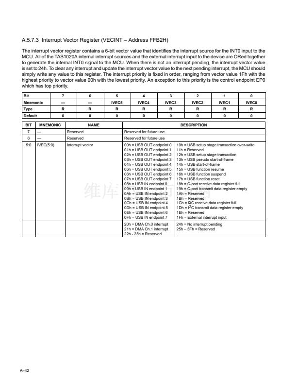
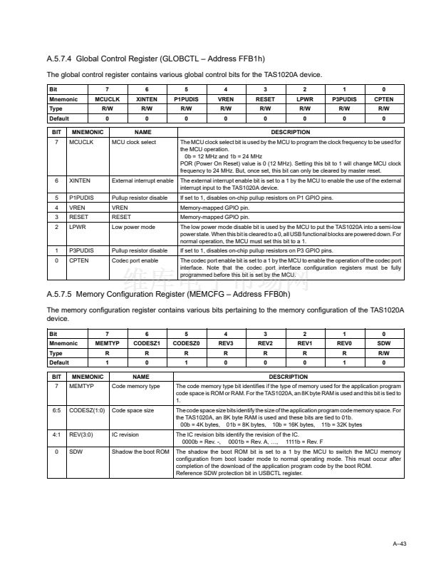
A.5.4.3 Codec port interface configuration register 3 (CPTCNF3 鈥?Address FFDEh)
The codec port interface configuration register 3 is used to store various control bits for the codec port interface
operation.
Bit
Mnemonic
Type
Default
BIT
7
MNEMONIC
DDLY
7
DDLY
R/W
0
6
TRSEN
R/W
0
NAME
Data delay
5
CSCLKP
R/W
1
4
CSYNCP
R/W
1
3
CSYNCL
R/W
0
2
BYOR
R/W
0
DESCRIPTION
The data delay bit is set to a 1 by the MCU to program a one CSCLK cycle delay of the serial
data output and input signals in reference to the leading edge of the CSYNC signal. The
MCU must clear this bit to a 0 for no delay between these signals.
The 3-state enable bit is set to a 1 by the MCU to program the hardware to set the serial
data output signal to the high-impedance state for the time slots during the audio frame that
are not valid. The MCU must clear this bit to a 0 to program the hardware to use
zero-padding for the serial data output signal for time slots during the audio frame that are
not valid.
The CSCLK polarity bit is used by the MCU to program the clock edge used for the codec
port interface frame sync (CSYNC) output signal, codec port interface serial data output
(CDATO) signal and codec port interface serial data Input (CDATI) signal. When this bit is
set to a 1, the CSYNC signal is generated with the negative edge of the codec port interface
serial clock (CSCLK) signal. Also, when this bit is set to a 1, the CDATO signal is generated
with the negative edge of the CSCLK signal and the CDATI signal is sampled with the
positive edge of the CSCLK signal. When this bit is cleared to a 0, the CSYNC signal is
generated with the positive edge of the CSCLK signal. Also, when this bit is cleared to a 0,
the CDATO signal is generated with the positive edge of the CSCLK signal and the CDATI
signal is sampled with the negative edge of the CSCLK signal.
The CSYNC polarity bit is set to a 1 by the MCU to program the polarity of the codec port
interface frame sync (CSYNC) output signal to be active high. The MCU must clear this bit
to a 0 to program the polarity of the CSYNC output signal to be active low.
The CSYNC length bit is set to a 1 by the MCU to program the length of the codec port
interface frame sync (CSYNC) output signal to be the same number of CSCLK cycles as
time slot 0. The MCU must clear this bit to a 0 to program the length of the CSYNC output
signal to be one CSCLK cycle.
The byte order bit is used by the MCU to program the byte order for the data moved by the
DMA between the USB endpoint buffer and the codec port interface. When this bit is set to
a 1, the byte order of each audio sample is reversed when the data is moved to/from the
USB endpoint buffer. When this bit is cleared to a 0, the byte order of the each audio sample
is unchanged.
The CSCLK direction bit is set to a 1 by the MCU to program the direction of the codec port
interface serial clock (CSCLK) signal as an input to the TAS1020A device. The MCU must
clear this bit to a 0 to program the direction of the CSCLK signal as an output from the
TAS1020A device.
The CSYNC direction bit is set to a 1 by the MCU to program the direction of the codec port
interface frame sync (CSYNC) signal as an input to the TAS1020A device. The MCU must
clear this bit to a 0 to program the direction of the CSYNC signal as an output from the
TAS1020A device.
1
CSCLKD
R/W
0
0
CSYNCD
R/W
0
6
TRSEN
3-State enable
5
CSCLKP
CSCLK polarity
4
CSYNCP
CSYNC polarity
3
CSYNCL
CSYNC length
2
BYOR
Byte order
1
CSCLKD
CSCLK direction
0
CSYNCD
CSYNC direction
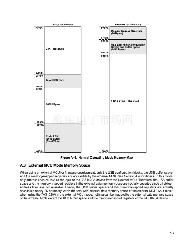
A鈥?1


 1
1
 2
2
 3
3
 4
4
 5
5
 6
6
 7
7
 8
8
 9
9
 10
10
 11
11
 12
12
 13
13
 14
14
 15
15
 16
16
 17
17
 18
18
 19
19
 20
20
 21
21
 22
22
 23
23
 24
24
 25
25
 26
26
 27
27
 28
28
 29
29
 30
30
 31
31
 32
32
 33
33
 34
34
 35
35
 36
36
 37
37
 38
38
 39
39
 40
40
 41
41
 42
42
 43
43
 44
44
 45
45
 46
46
 47
47
 48
48
 49
49
 50
50
 51
51
 52
52
 53
53
 54
54
 55
55
 56
56
 57
57
 58
58
 59
59
 60
60
 61
61
 62
62
 63
63
 64
64
 65
65
 66
66
 67
67
 68
68
 69
69
 70
70
 71
71
 72
72
 73
73
 74
74
 75
75
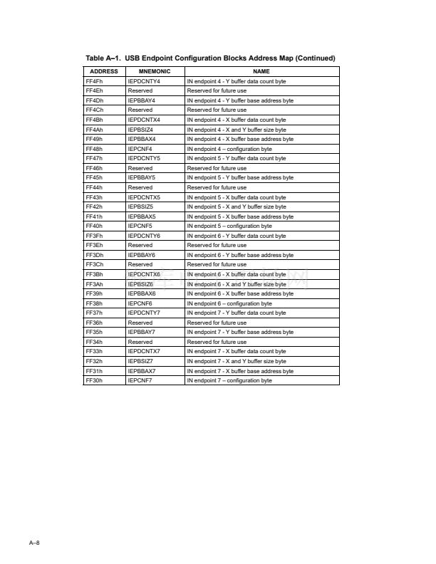 76
76
 77
77
 78
78
 79
79
 80
80
 81
81
 82
82
 83
83
 84
84
 85
85
 86
86
 87
87
 88
88
 89
89
 90
90
 91
91
 92
92
 93
93
 94
94
 95
95
 96
96
 97
97
 98
98
 99
99
 100
100
 101
101
 102
102
 103
103
 104
104
 105
105
 106
106
 107
107
 108
108
 109
109
 110
110
 111
111
 112
112
 113
113
 114
114
