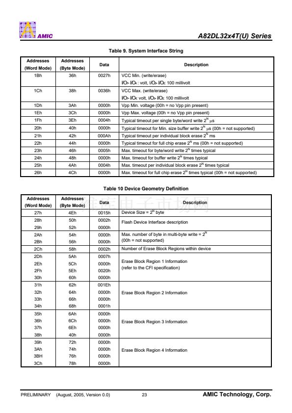
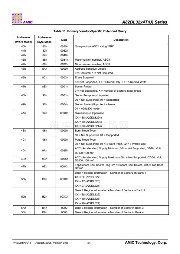
16 bits each or 4,194,304 bytes of 8 bits each. Word mode
鈥?/div>
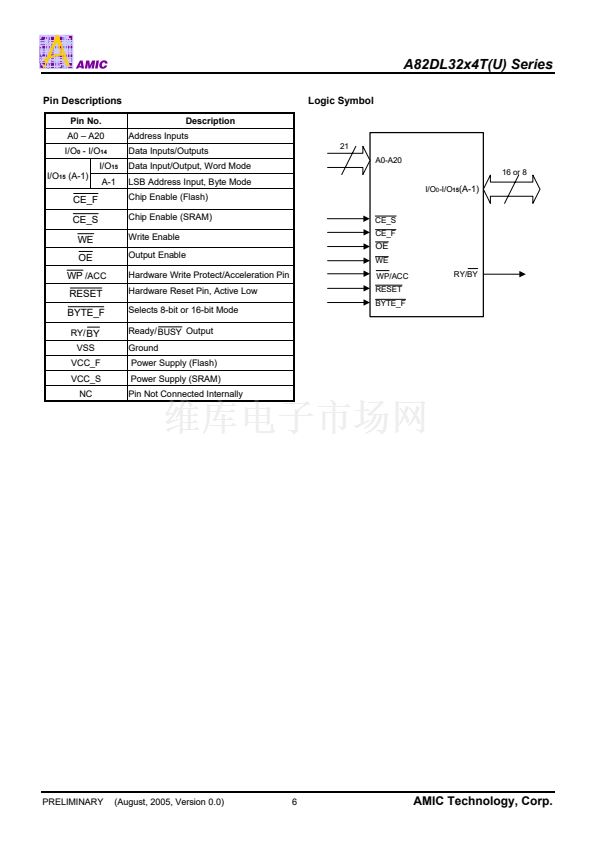
I/O
7
. The device is designed to be programmed in-system
with the standard 3.0 volt VCC supply, and can also be
programmed in standard EPROM programmers.
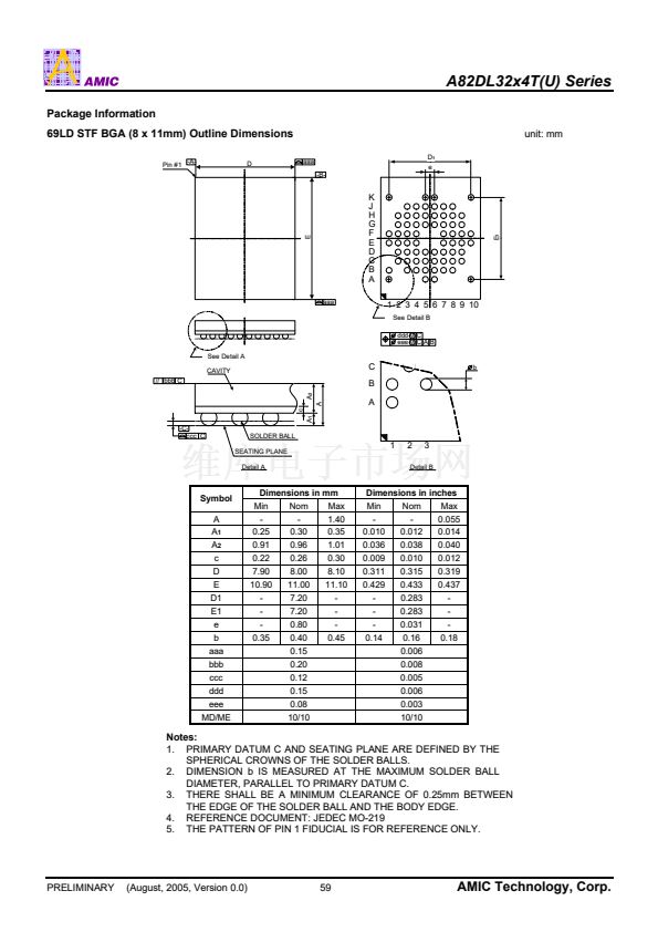
The device is available with an access time of 70ns. The
devices are offered in 69-ball Fine-pitch BGA. Standard
control pins鈥攃hip enable (
CE_F
), write enable (
WE
), and
output enable (
OE
)鈥攃ontrol normal read and write
operations, and avoid bus contention issues.
The device requires only a
single 3.0 volt power supply
for
both read and write functions. Internally generated and
regulated voltages are provided for the program and erase
operations.
A82DL32x4T(U) Features
The device offers complete compatibility with the
JEDEC
single-power-supply Flash command set standard.
Commands are written to the command register using
standard microprocessor write timings. Reading data out of
the device is similar to reading from other Flash or EPROM
devices.
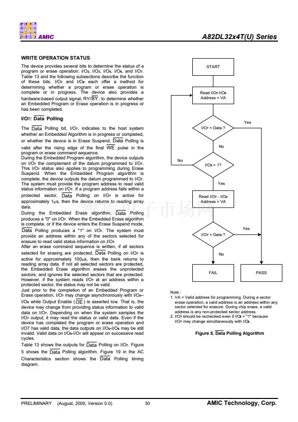
The host system can detect whether a program or erase
operation is complete by using the device
status bits:
RY/
BY
pin, I/O
7
(
Data
Polling) and I/O
6
/I/O
2
(toggle bits).
After a program or erase cycle has been completed, the
device automatically returns to reading array data.
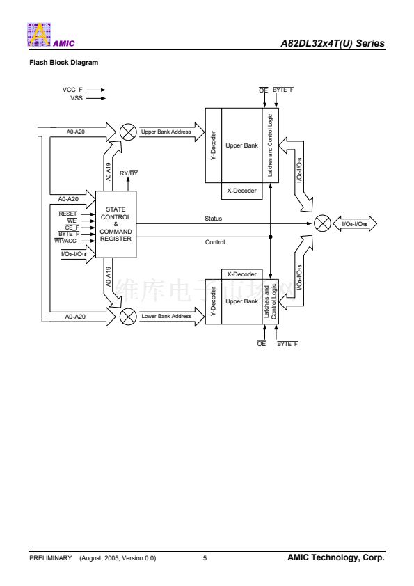
The
sector erase architecture
allows memory sectors to be
erased and reprogrammed without affecting the data
contents of other sectors. The device is fully erased when
shipped from the factory.
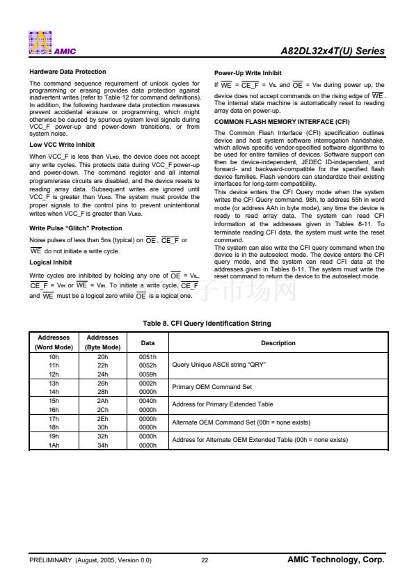
Hardware data protection
measures include a low VCC
detector that automatically inhibits write operations during
power transitions. The
hardware sector protection
feature
disables both program and erase operations in any
combination of the sectors of memory. This can be achieved
in-s y s t e m or via programming equipment.
The device offers two power-saving features. When
addresses have been stable for a specified amount of time,
the device enters the
automatic sleep mode.
The system
can also place the device into the
standby mode.
Power
consumption is greatly reduced in both modes.
Simultaneous Read/Write Operations with Zero
Latency
The Simultaneous Read/Write architecture provides
simultaneous operation
by dividing the memory space into
two banks. The device can improve overall system
performance by allowing a host system to program or erase
in one bank, then immediately and simultaneously read from
the other bank, with zero latency. This releases the system
from waiting for the completion of program or erase
operations.
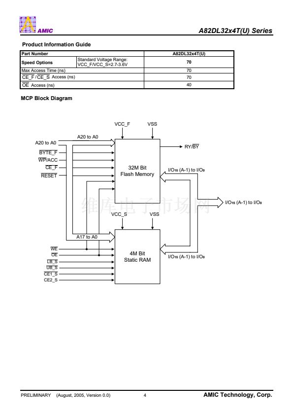
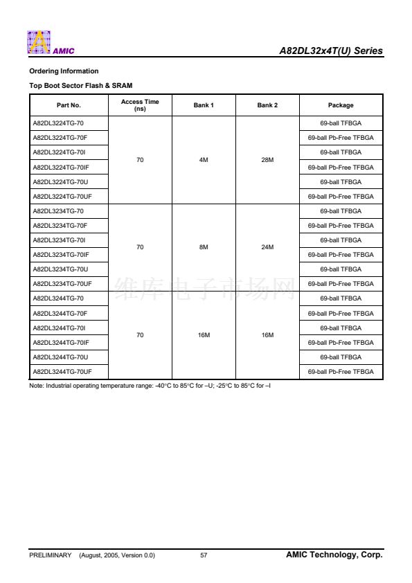
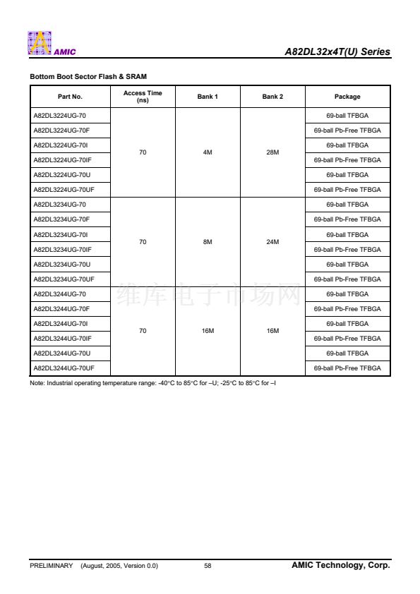
The A82DL32x4T(U) devices uses multiple bank archi-
tectures to provide flexibility for different applications. Three
devices are available with these bank sizes:
Device
DL3224
DL3234
DL3244
Bank 1
4 Mb
8 Mb
16 Mb
Bank 2
28 Mb
24 Mb
16 Mb
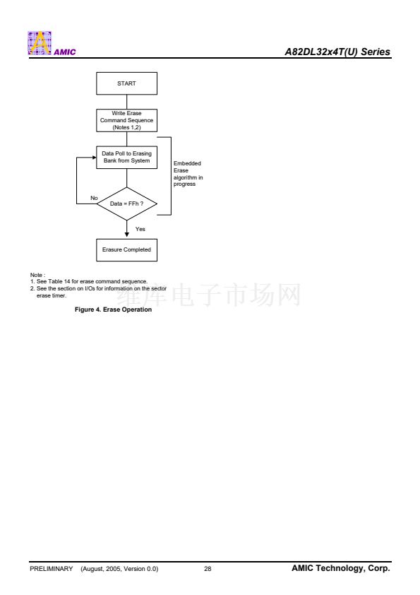
PRELIMINARY
(August, 2005, Version 0.0)
2
AMIC Technology, Corp.


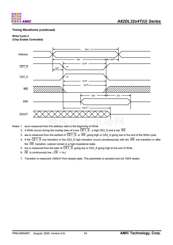
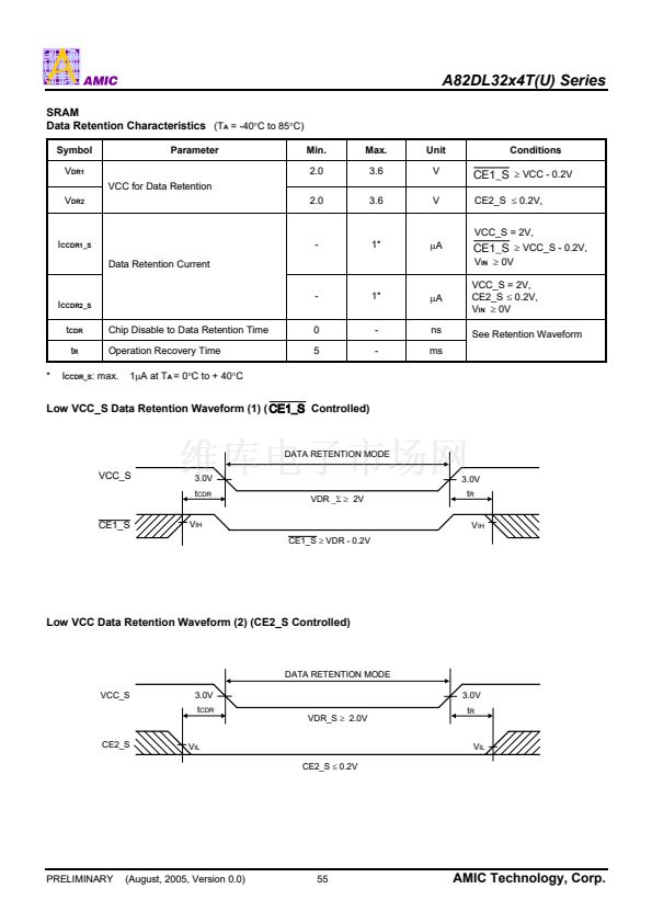
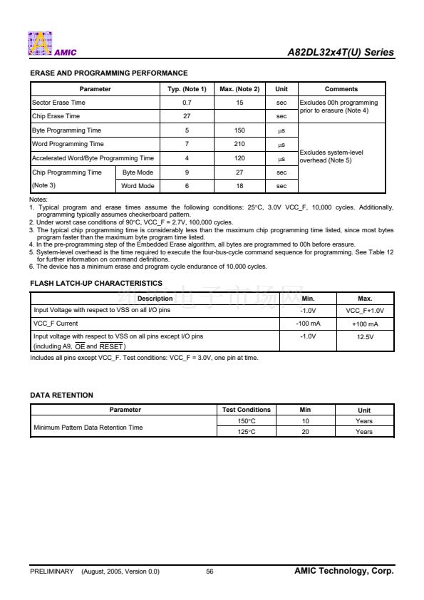
 1
1
 2
2
 3
3
 4
4
 5
5
 6
6
 7
7
 8
8
 9
9
 10
10
 11
11
 12
12
 13
13
 14
14
 15
15
 16
16
 17
17
 18
18
 19
19
 20
20
 21
21
 22
22
 23
23
 24
24
 25
25
 26
26
 27
27
 28
28
 29
29
 30
30
 31
31
 32
32
 33
33
 34
34
 35
35
 36
36
 37
37
 38
38
 39
39
 40
40
 41
41
 42
42
 43
43
 44
44
 45
45
 46
46
 47
47
 48
48
 49
49
 50
50
 51
51
 52
52
 53
53
 54
54
 55
55
 56
56
 57
57
 58
58
 59
59
 60
60
