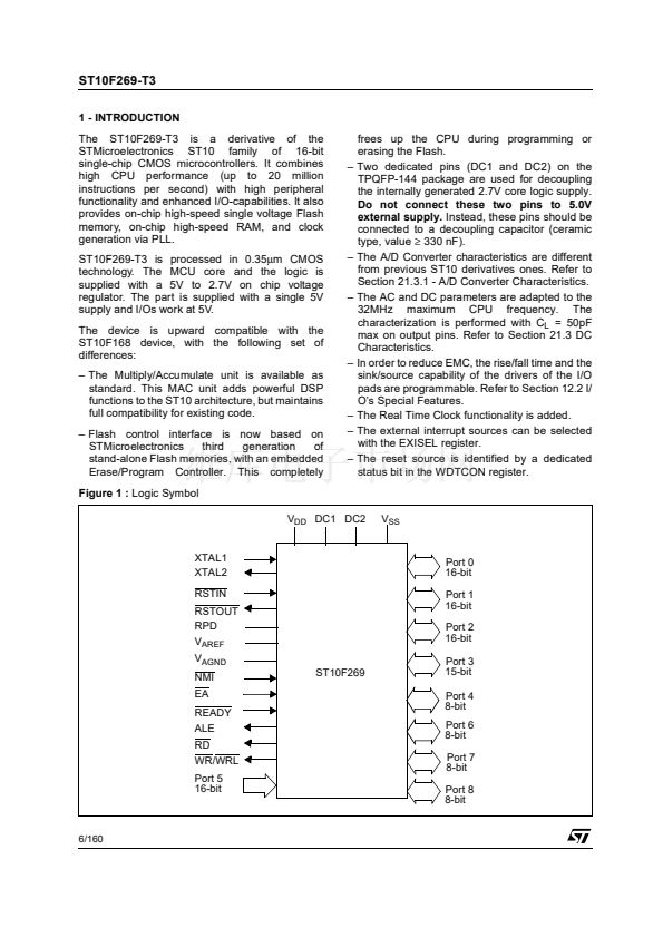
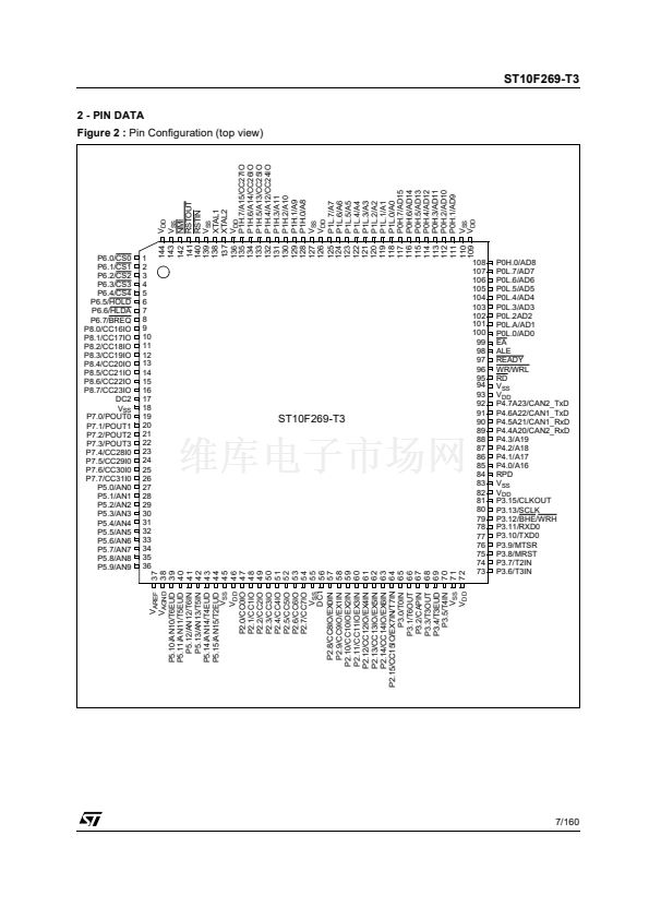
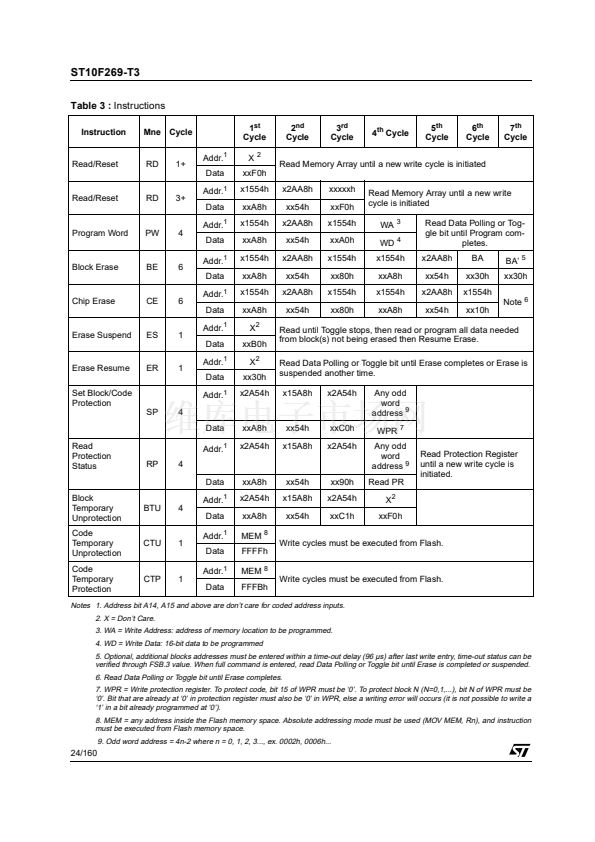
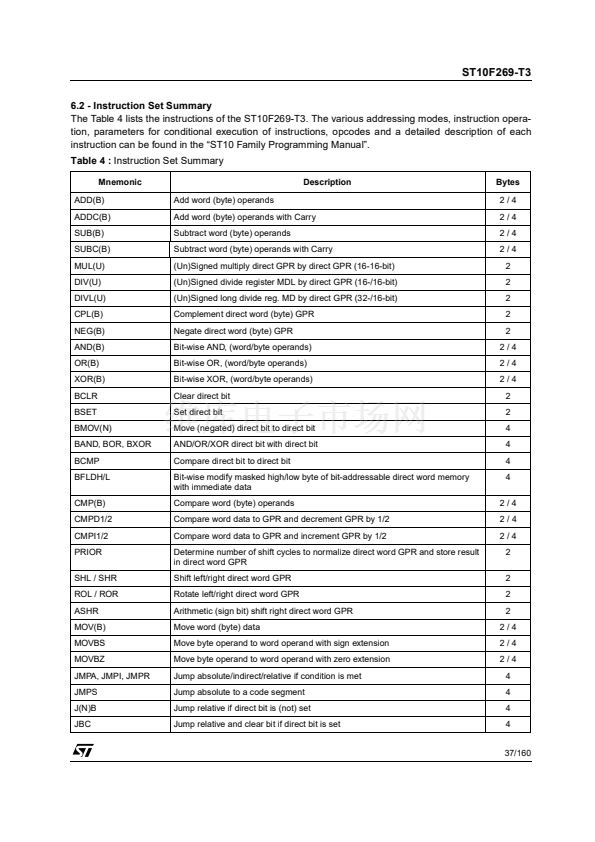
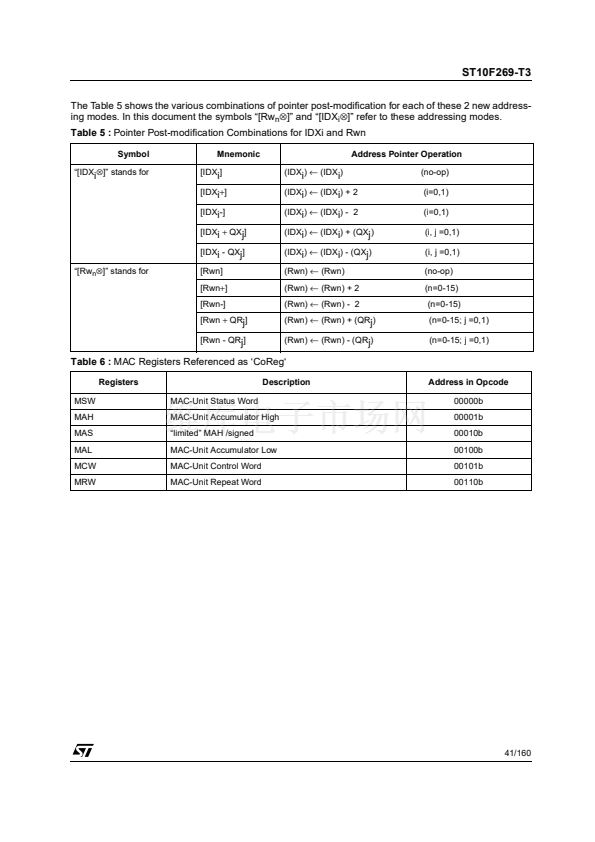
Addr.
Addr.
Addr.
Addr.
Addr.
Addr.
Addr.
Addr.
Addr.
Addr.
Addr.
Addr.
pletes.
BA鈥?/div>
5
xx30h
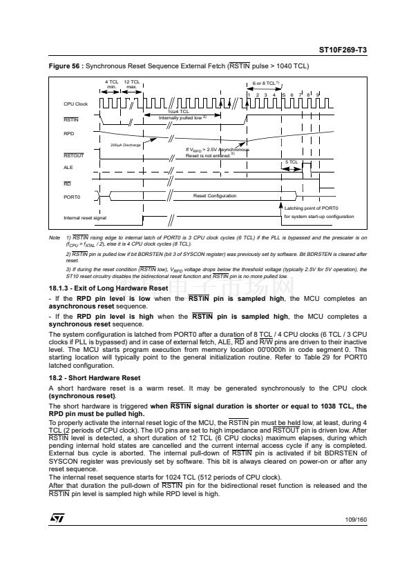
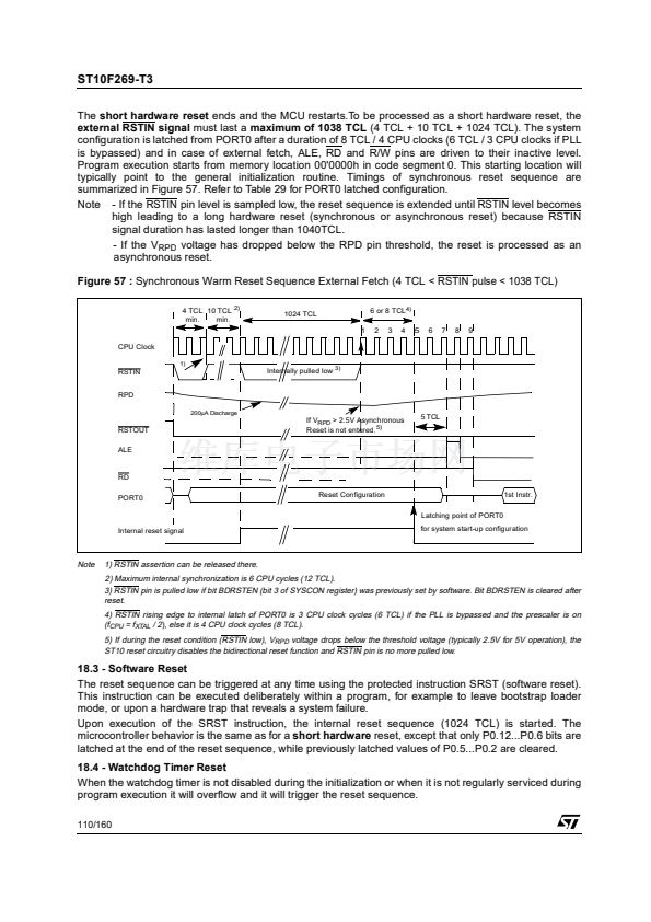
Note
6
2
nd
Cycle
3
rd
Cycle
4
th
Cycle
5
th
Cycle
6
th
Cycle
7
th
Cycle
Read/Reset
RD
1+
Read Memory Array until a new write cycle is initiated
Block Erase
BE
6
Read until Toggle stops, then read or program all data needed
from block(s) not being erased then Resume Erase.
Read Data Polling or Toggle bit until Erase completes or Erase is
suspended another time.
x15A8h
x2A54h
Any odd
word
address
9
WPR
7
Any odd
word
address
9
Read PR
X
2
xxF0h
Read Protection Register
until a new write cycle is
initiated.
CTU
1
Write cycles must be executed from Flash.
CTP
1
Write cycles must be executed from Flash.
Notes 1. Address bit A14, A15 and above are don鈥檛 care for coded address inputs.
2. X = Don鈥檛 Care.
3. WA = Write Address: address of memory location to be programmed.
4. WD = Write Data: 16-bit data to be programmed
5. Optional, additional blocks addresses must be entered within a time-out delay (96 碌s) after last write entry, time-out status can be
verified through FSB.3 value. When full command is entered, read Data Polling or Toggle bit until Erase is completed or suspended.
6. Read Data Polling or Toggle bit until Erase completes.
7. WPR = Write protection register. To protect code, bit 15 of WPR must be 鈥?鈥? To protect block N (N=0,1,...), bit N of WPR must be
鈥?鈥? Bit that are already at 鈥?鈥?in protection register must also be 鈥?鈥?in WPR, else a writing error will occurs (it is not possible to write a
鈥?鈥?in a bit already programmed at 鈥?鈥?.
8. MEM = any address inside the Flash memory space. Absolute addressing mode must be used (MOV MEM, Rn), and instruction
must be executed from Flash memory space.
9. Odd word address = 4n-2 where n = 0, 1, 2, 3..., ex. 0002h, 0006h...
24/160


 1
1
 2
2
 3
3
 4
4
 5
5
 6
6
 7
7
 8
8
 9
9
 10
10
 11
11
 12
12
 13
13
 14
14
 15
15
 16
16
 17
17
 18
18
 19
19
 20
20
 21
21
 22
22
 23
23
 24
24
 25
25
 26
26
 27
27
 28
28
 29
29
 30
30
 31
31
 32
32
 33
33
 34
34
 35
35
 36
36
 37
37
 38
38
 39
39
 40
40
 41
41
 42
42
 43
43
 44
44
 45
45
 46
46
 47
47
 48
48
 49
49
 50
50
 51
51
 52
52
 53
53
 54
54
 55
55
 56
56
 57
57
 58
58
 59
59
 60
60
 61
61
 62
62
 63
63
 64
64
 65
65
 66
66
 67
67
 68
68
 69
69
 70
70
 71
71
 72
72
 73
73
 74
74
 75
75
 76
76
 77
77
 78
78
 79
79
 80
80
 81
81
 82
82
 83
83
 84
84
 85
85
 86
86
 87
87
 88
88
 89
89
 90
90
 91
91
 92
92
 93
93
 94
94
 95
95
 96
96
 97
97
 98
98
 99
99
 100
100
 101
101
 102
102
 103
103
 104
104
 105
105
 106
106
 107
107
 108
108
 109
109
 110
110
 111
111
 112
112
 113
113
 114
114
 115
115
 116
116
 117
117
 118
118
 119
119
 120
120
 121
121
 122
122
 123
123
 124
124
 125
125
 126
126
 127
127
 128
128
 129
129
 130
130
 131
131
 132
132
 133
133
 134
134
 135
135
 136
136
 137
137
 138
138
 139
139
 140
140
 141
141
 142
142
 143
143
 144
144
 145
145
 146
146
 147
147
 148
148
 149
149
 150
150
 151
151
 152
152
 153
153
 154
154
 155
155
 156
156
 157
157
 158
158
 159
159
 160
160
