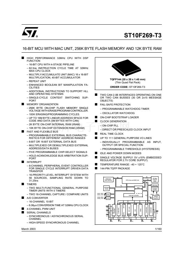
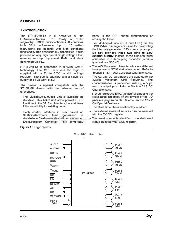
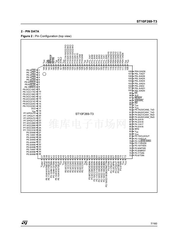
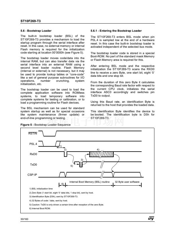
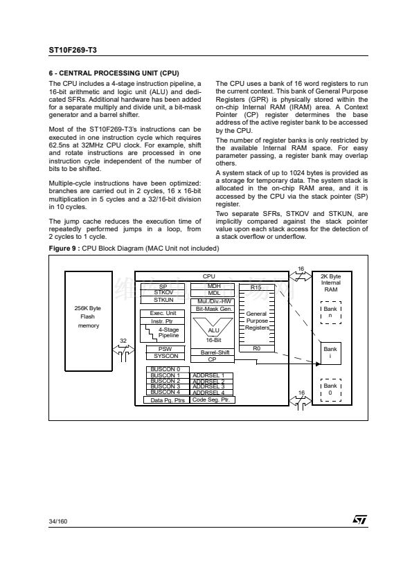
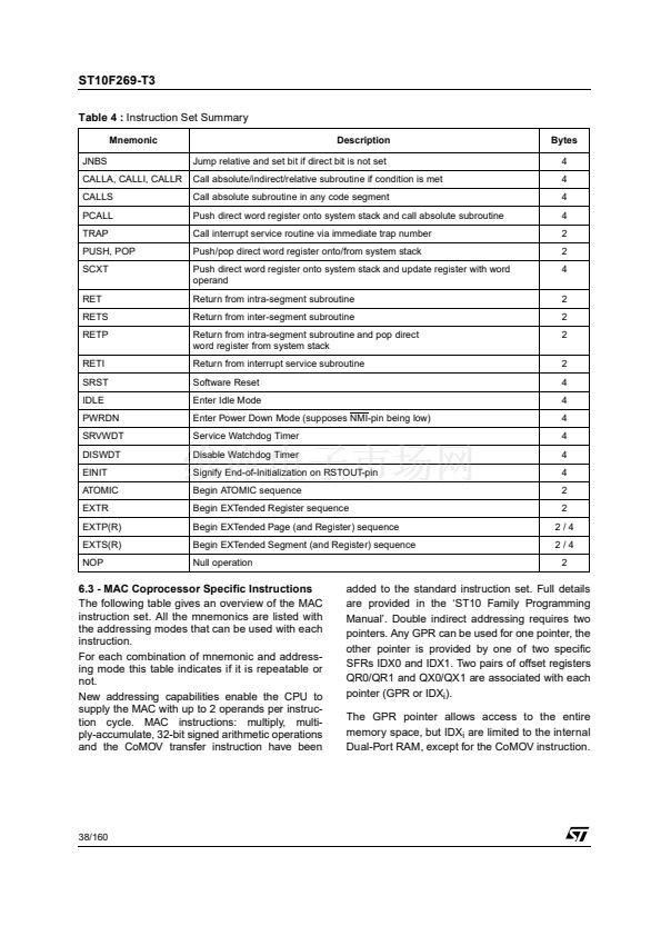
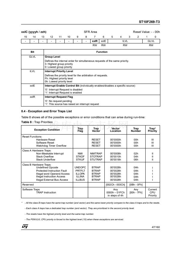
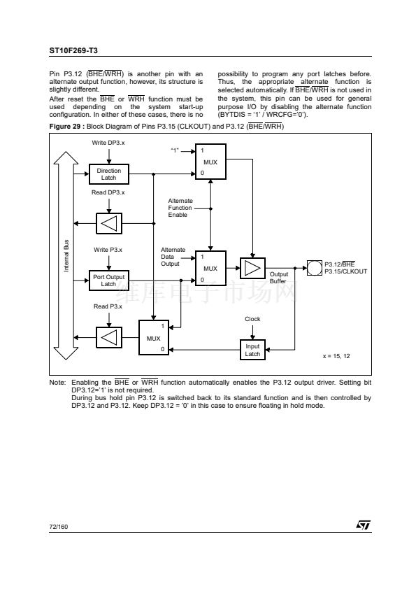
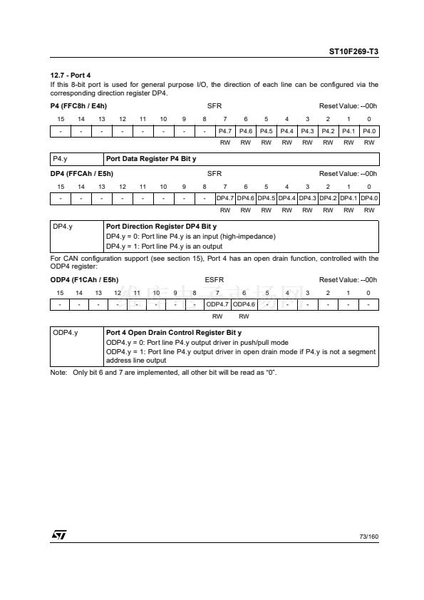
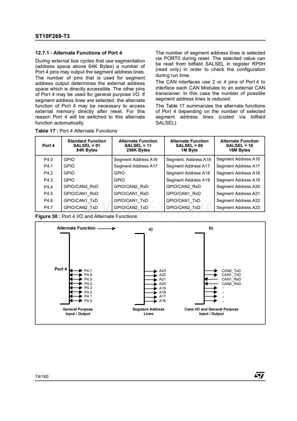
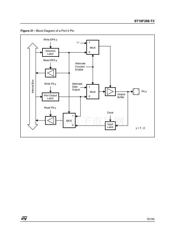
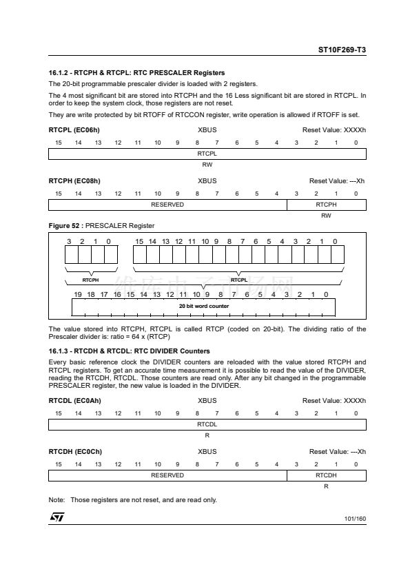
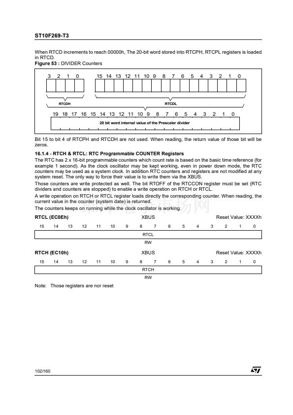
鈥?鈥?/div>
8011h
Acc. to 鈥?0鈥?Byte
DP3.10:
In this case, the watchdog timer is disabled, so the
bootstrap loading sequence is not time limited.
Pin TXD0 is configured as output, so the
ST10F269-T3 can return the identification Byte.
Even if the internal Flash is enabled, no code can
be executed out of it.
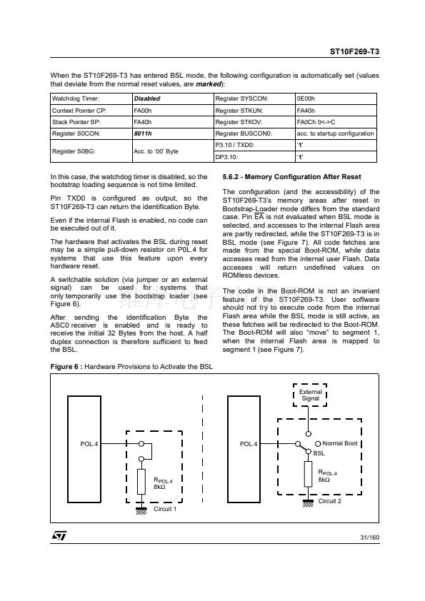
The hardware that activates the BSL during reset
may be a simple pull-down resistor on P0L.4 for
systems that use this feature upon every
hardware reset.
A switchable solution (via jumper or an external
signal) can be used for systems that
only temporarily use the bootstrap loader (see
Figure 6).
After sending the identification Byte the
ASC0 receiver is enabled and is ready to
receive the initial 32 Bytes from the host. A half
duplex connection is therefore sufficient to feed
the BSL.
Figure 6 :
Hardware Provisions to Activate the BSL
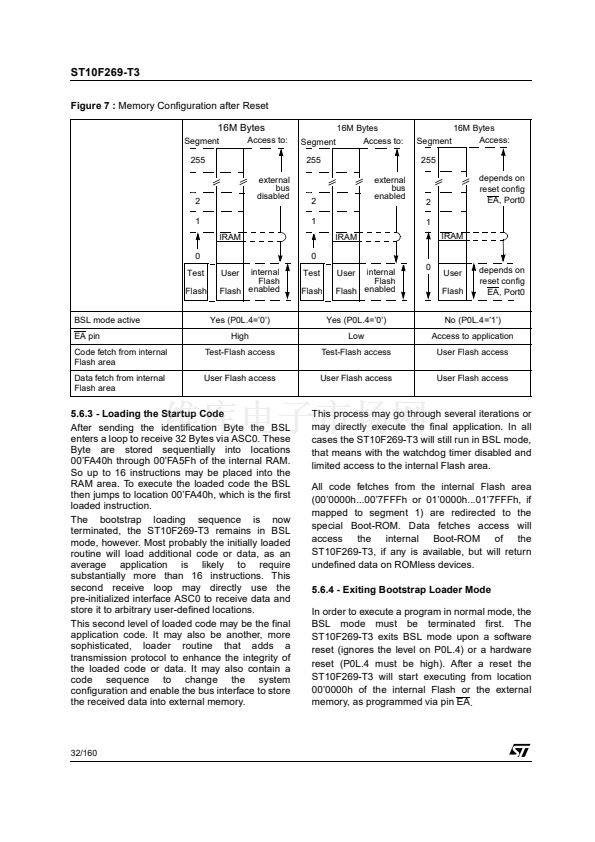
5.6.2 - Memory Configuration After Reset
The configuration (and the accessibility) of the
ST10F269-T3鈥檚 memory areas after reset in
Bootstrap-Loader mode differs from the standard
case. Pin EA is not evaluated when BSL mode is
selected, and accesses to the internal Flash area
are partly redirected, while the ST10F269-T3 is in
BSL mode (see Figure 7). All code fetches are
made from the special Boot-ROM, while data
accesses read from the internal user Flash. Data
accesses will return undefined values on
ROMless devices.
The code in the Boot-ROM is not an invariant
feature of the ST10F269-T3. User software
should not try to execute code from the internal
Flash area while the BSL mode is still active, as
these fetches will be redirected to the Boot-ROM.
The Boot-ROM will also 鈥渕ove鈥?to segment 1,
when the internal Flash area is mapped to
segment 1 (see Figure 7).
External
Signal
POL.4
POL.4
Normal Boot
BSL
R
POL.4
8k鈩?/div>
R
POL.4
8k鈩?/div>
Circuit 2
Circuit 1
31/160


 1
1
 2
2
 3
3
 4
4
 5
5
 6
6
 7
7
 8
8
 9
9
 10
10
 11
11
 12
12
 13
13
 14
14
 15
15
 16
16
 17
17
 18
18
 19
19
 20
20
 21
21
 22
22
 23
23
 24
24
 25
25
 26
26
 27
27
 28
28
 29
29
 30
30
 31
31
 32
32
 33
33
 34
34
 35
35
 36
36
 37
37
 38
38
 39
39
 40
40
 41
41
 42
42
 43
43
 44
44
 45
45
 46
46
 47
47
 48
48
 49
49
 50
50
 51
51
 52
52
 53
53
 54
54
 55
55
 56
56
 57
57
 58
58
 59
59
 60
60
 61
61
 62
62
 63
63
 64
64
 65
65
 66
66
 67
67
 68
68
 69
69
 70
70
 71
71
 72
72
 73
73
 74
74
 75
75
 76
76
 77
77
 78
78
 79
79
 80
80
 81
81
 82
82
 83
83
 84
84
 85
85
 86
86
 87
87
 88
88
 89
89
 90
90
 91
91
 92
92
 93
93
 94
94
 95
95
 96
96
 97
97
 98
98
 99
99
 100
100
 101
101
 102
102
 103
103
 104
104
 105
105
 106
106
 107
107
 108
108
 109
109
 110
110
 111
111
 112
112
 113
113
 114
114
 115
115
 116
116
 117
117
 118
118
 119
119
 120
120
 121
121
 122
122
 123
123
 124
124
 125
125
 126
126
 127
127
 128
128
 129
129
 130
130
 131
131
 132
132
 133
133
 134
134
 135
135
 136
136
 137
137
 138
138
 139
139
 140
140
 141
141
 142
142
 143
143
 144
144
 145
145
 146
146
 147
147
 148
148
 149
149
 150
150
 151
151
 152
152
 153
153
 154
154
 155
155
 156
156
 157
157
 158
158
 159
159
 160
160
