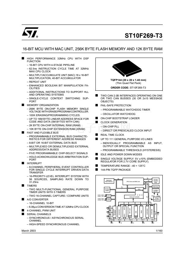
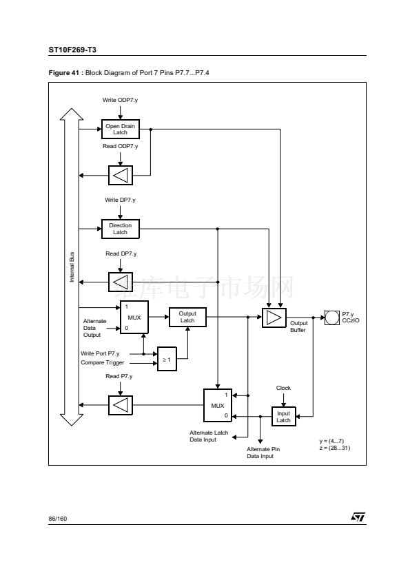
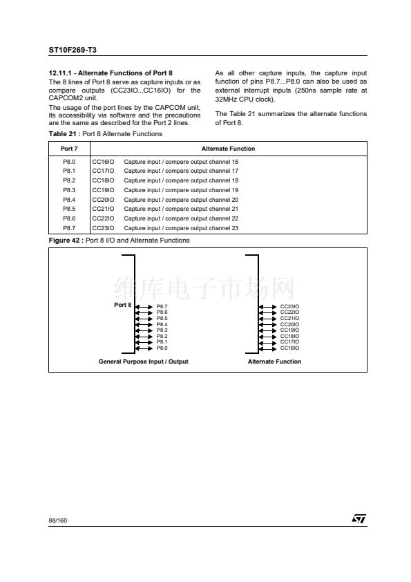
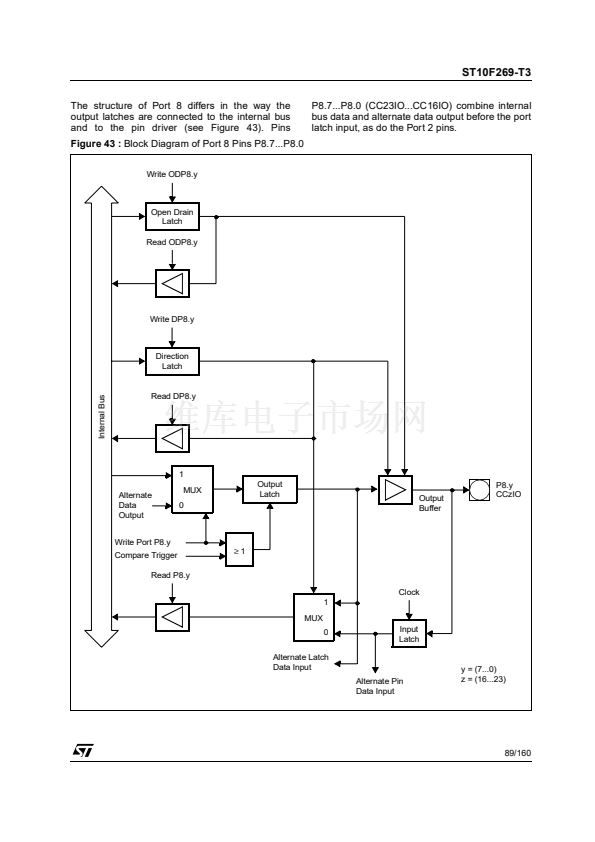
ST10F269-T3
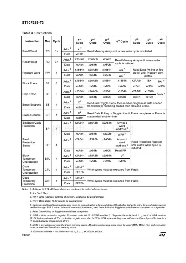
鈥?Generally, command sequences cannot be
written to Flash by instructions fetched from the
Flash itself. Thus, the Flash commands must be
written by instructions, executed from internal
RAM or external memory.
鈥?Command cycles on the CPU interface need not
to be consecutively received (pauses allowed).
The CPU interface delivers dummy read data for
not used cycles within command sequences.
鈥?All addresses of command cycles shall be
defined only with
Register-indirect
addressing
mode in the according move instructions. Direct
addressing is not allowed for command
sequences. Address segment or data page
pointer are taken into account for the command
address value.
5.3.7 - Reset Processing and Initial State
The Flash module distinguishes two kinds of CPU
reset types
The lengthening of CPU reset:
鈥?Is not reported to external devices by
bidirectional pin
鈥?Is not enabled in case of external start of CPU
after reset.
5.4 - Flash Memory Configuration
The default memory configuration of the
ST10F269-T3 Memory is determined by the state
of the EA pin at reset. This value is stored in the
Internal ROM Enable bit (named ROMEN) of the
SYSCON register.
When ROMEN = 0, the internal Flash is disabled
and external ROM is used for startup control.
Flash memory can later be enabled by setting the
ROMEN bit of SYSCON to 1. The code
performing this setting must not run from a
segment of the external ROM to be replaced by a
segment of the Flash memory, otherwise
unexpected behaviour may occur.
For example, if external ROM code is located in
the first 32K Bytes of segment 0, the first
32K Bytes of the Flash must then be enabled in
segment 1. This is done by setting the ROMS1 bit
of SYSCON to 0 before or simultaneously with
setting of ROMEN bit. This must be done in the
externally supplied program before the execution
of the EINIT instruction.
If program execution starts from external memory,
but access to the Flash memory mapped in
segment 0 is later required, then the code that
performs the setting of ROMEN bit must be
executed either in the segment 0 but above
address 00鈥?000h, or from the internal RAM.
Bit ROMS1 only affects the mapping of the first
32K Bytes of the Flash memory. All other parts of
the Flash memory (addresses 01鈥?000h -
04鈥橣FFFh) remain unaffected.
The SGTDIS Segmentation Disable / Enable must
also be set to 0 to allow the use of the full
256K Bytes of on-chip memory in addition to the
external boot memory. The correct procedure on
changing the segmentation registers must also be
observed to prevent an unwanted trap condition:
鈥?Instructions that configure the internal memory
must only be executed from external memory or
from the internal RAM.
鈥?An Absolute Inter-Segment Jump (JMPS)
instruction must be executed after Flash
enabling, to the next instruction, even if this next
instruction is located in the consecutive address.
鈥?Whenever the internal Memory is disabled,
enabled or remapped, the DPPs must be
explicitly (re)loaded to enable correct data
accesses to the internal memory and/or external
memory.
5.5 - Application Examples
5.5.1 - Handling of Flash Addresses
All command, Block, Data and register addresses
to the Flash have to be located within the active
Flash memory space. The active space is that
address range to which the physical Flash
addresses are mapped as defined by the user.
When using data page pointer (DPP) for block
addresses make sure that address bit A15 and
A14 of the block address are reflected in both
LSBs of the selected DPPS.
Note: - For Command Instructions, address bit
A14, A15, A16 and A17 are don鈥檛 care.
This simplify a lot the application software,
because it minimizes the use of DPP regis-
ters when using Command in the Com-
mand Interface.
- Direct addressing is not allowed for
Command sequence operations to the
Flash. Only Register-indirect addressing
can be used for command, block or
write-data accesses.
25/160


 1
1
 2
2
 3
3
 4
4
 5
5
 6
6
 7
7
 8
8
 9
9
 10
10
 11
11
 12
12
 13
13
 14
14
 15
15
 16
16
 17
17
 18
18
 19
19
 20
20
 21
21
 22
22
 23
23
 24
24
 25
25
 26
26
 27
27
 28
28
 29
29
 30
30
 31
31
 32
32
 33
33
 34
34
 35
35
 36
36
 37
37
 38
38
 39
39
 40
40
 41
41
 42
42
 43
43
 44
44
 45
45
 46
46
 47
47
 48
48
 49
49
 50
50
 51
51
 52
52
 53
53
 54
54
 55
55
 56
56
 57
57
 58
58
 59
59
 60
60
 61
61
 62
62
 63
63
 64
64
 65
65
 66
66
 67
67
 68
68
 69
69
 70
70
 71
71
 72
72
 73
73
 74
74
 75
75
 76
76
 77
77
 78
78
 79
79
 80
80
 81
81
 82
82
 83
83
 84
84
 85
85
 86
86
 87
87
 88
88
 89
89
 90
90
 91
91
 92
92
 93
93
 94
94
 95
95
 96
96
 97
97
 98
98
 99
99
 100
100
 101
101
 102
102
 103
103
 104
104
 105
105
 106
106
 107
107
 108
108
 109
109
 110
110
 111
111
 112
112
 113
113
 114
114
 115
115
 116
116
 117
117
 118
118
 119
119
 120
120
 121
121
 122
122
 123
123
 124
124
 125
125
 126
126
 127
127
 128
128
 129
129
 130
130
 131
131
 132
132
 133
133
 134
134
 135
135
 136
136
 137
137
 138
138
 139
139
 140
140
 141
141
 142
142
 143
143
 144
144
 145
145
 146
146
 147
147
 148
148
 149
149
 150
150
 151
151
 152
152
 153
153
 154
154
 155
155
 156
156
 157
157
 158
158
 159
159
 160
160
