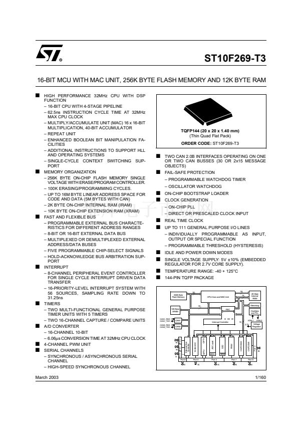
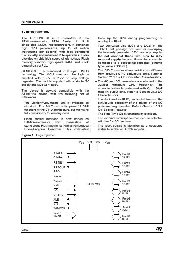
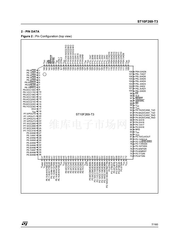
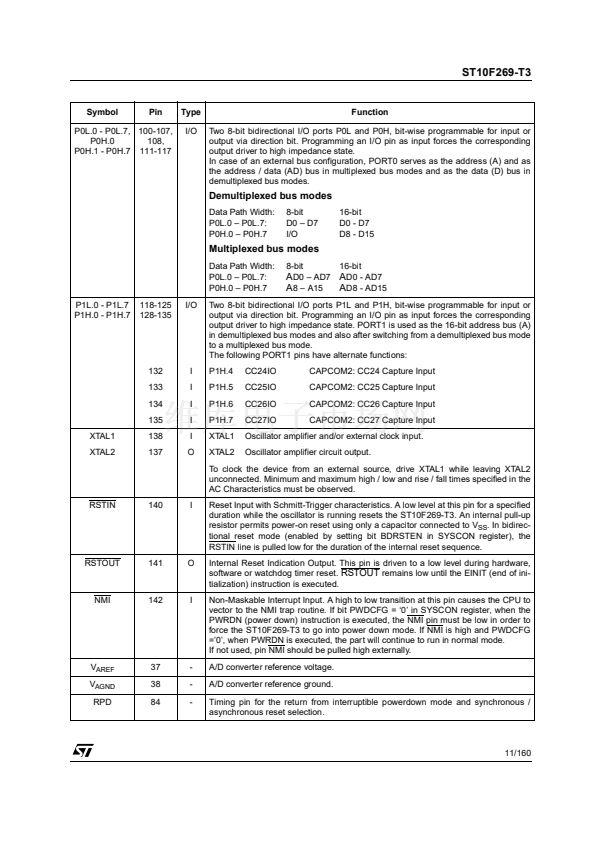
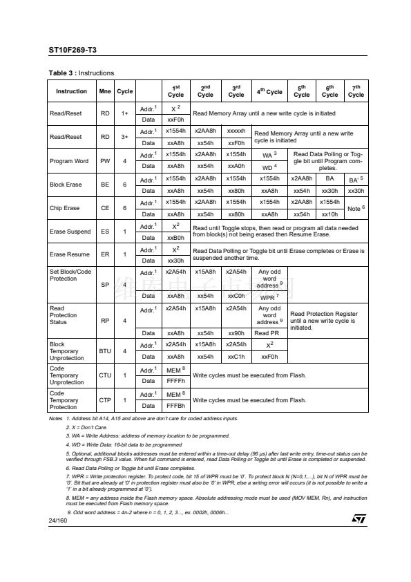
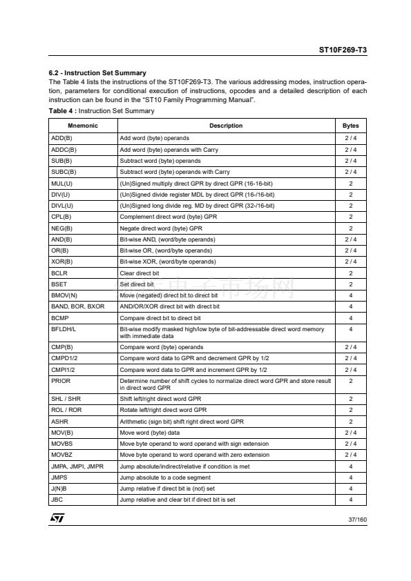
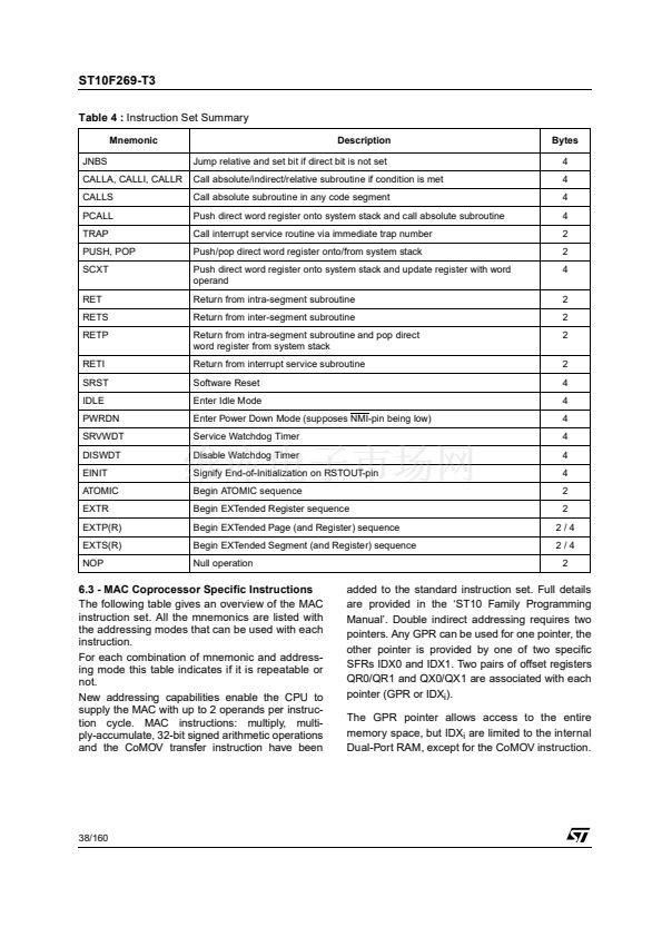
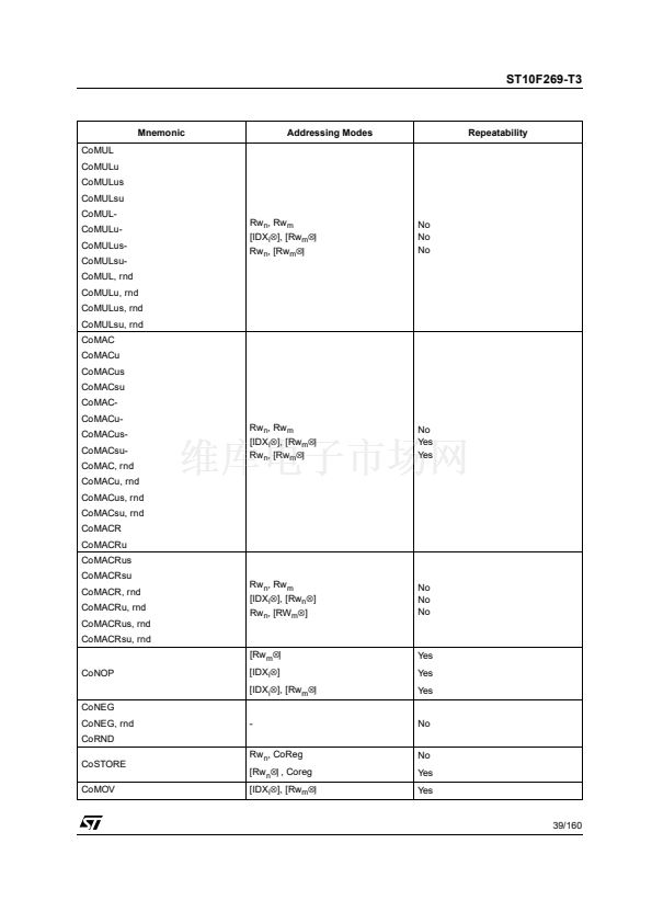
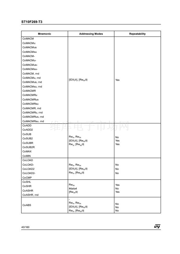
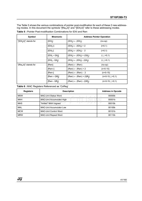
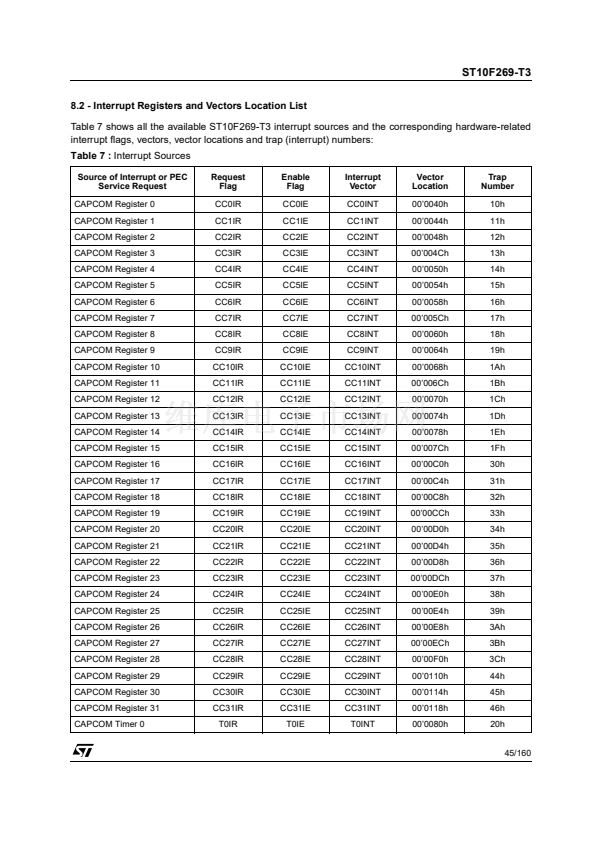
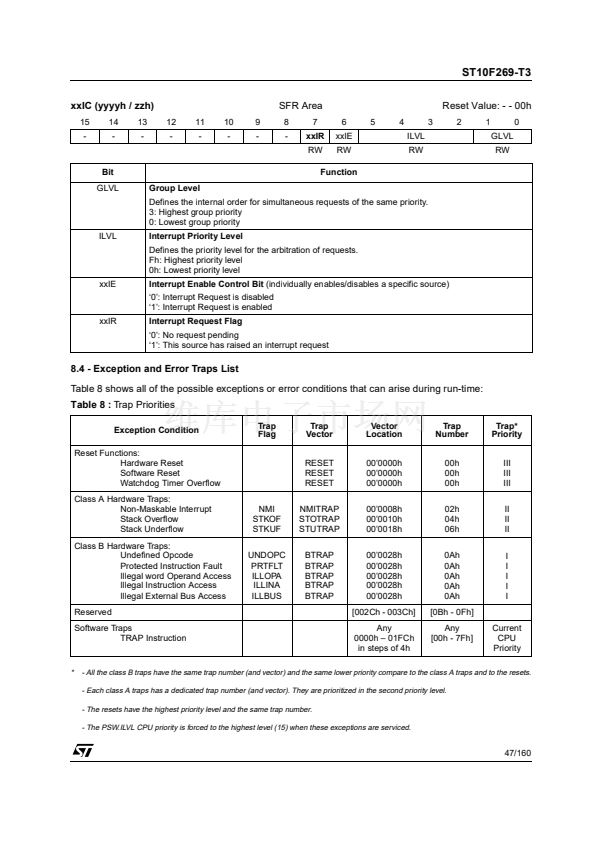
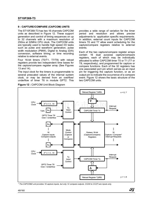
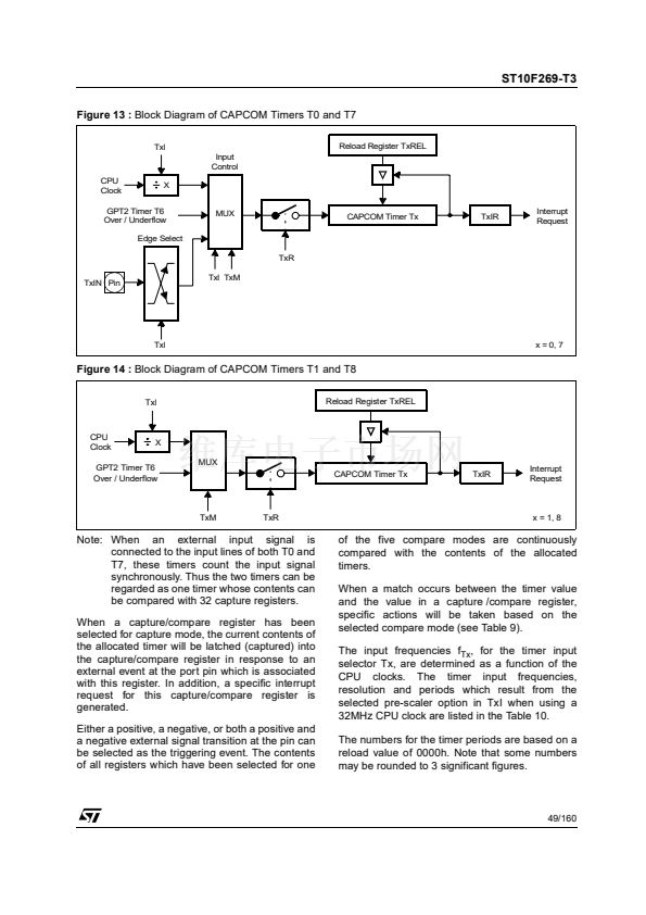
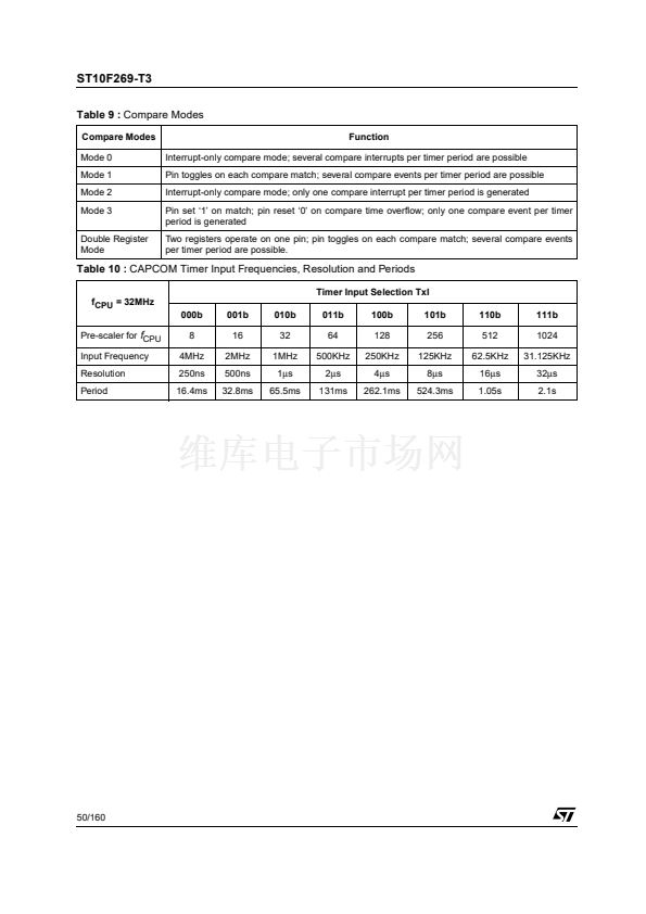
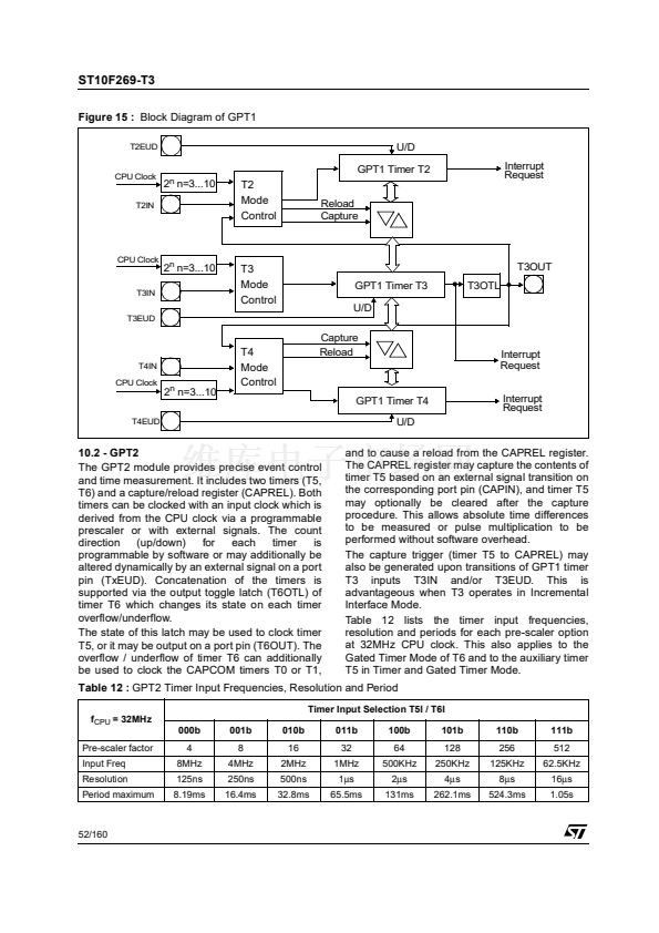
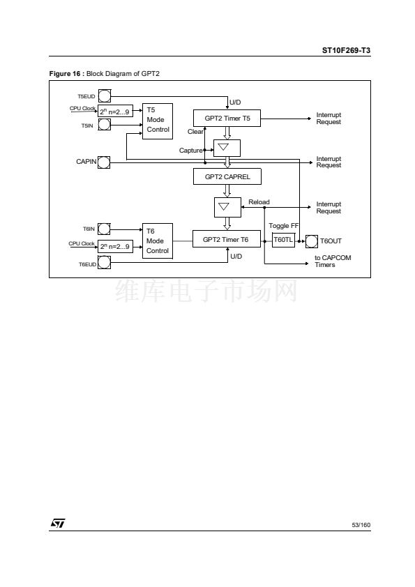
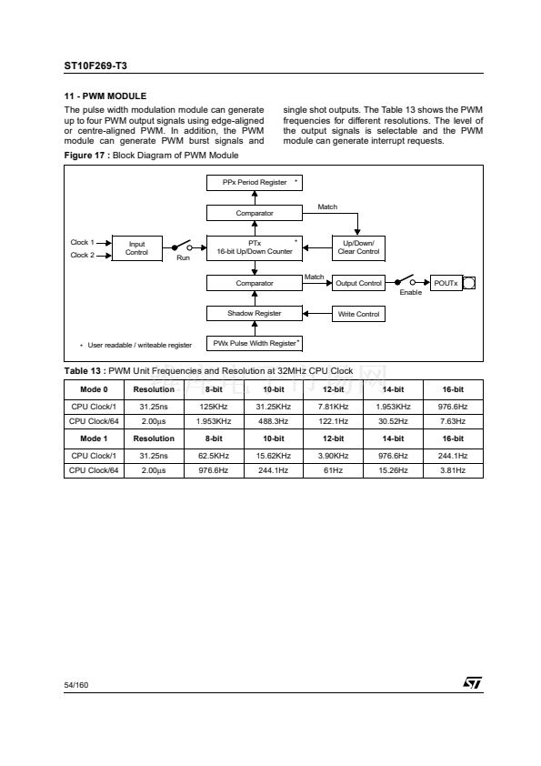
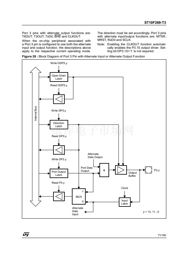
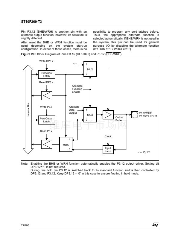
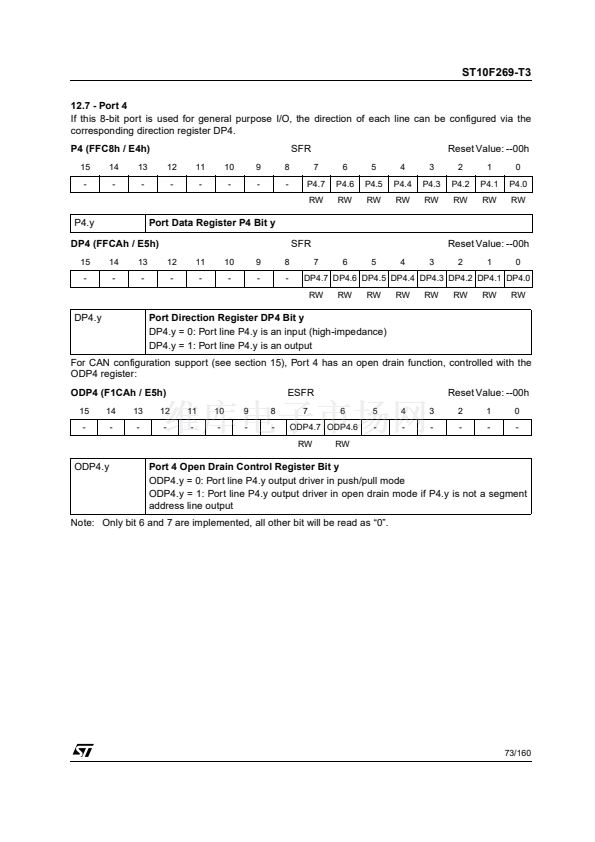
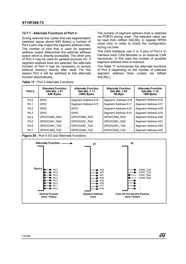
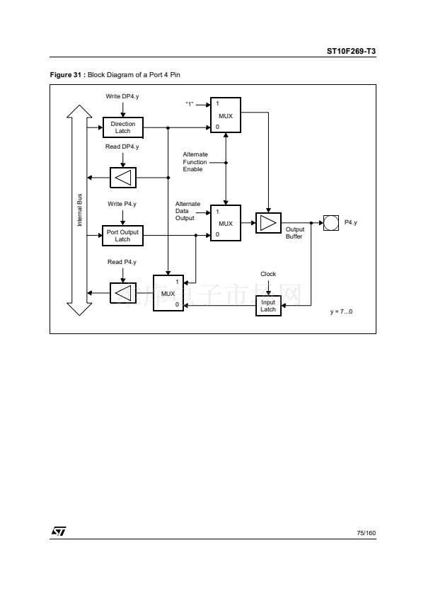
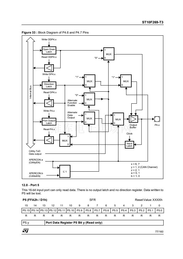
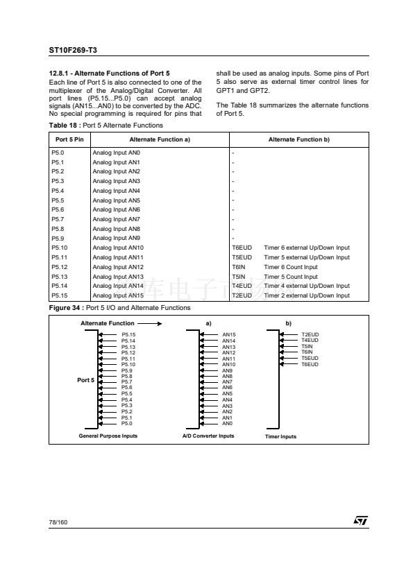
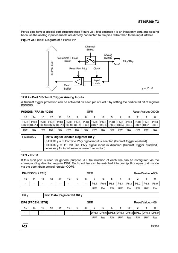
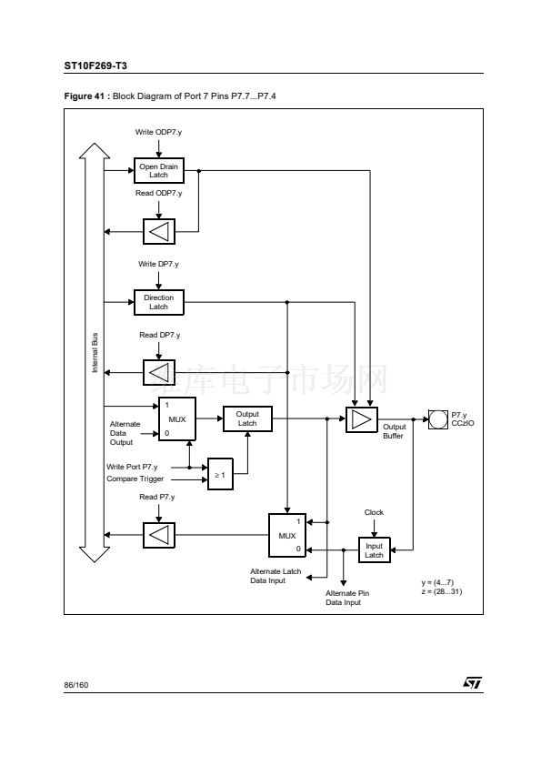
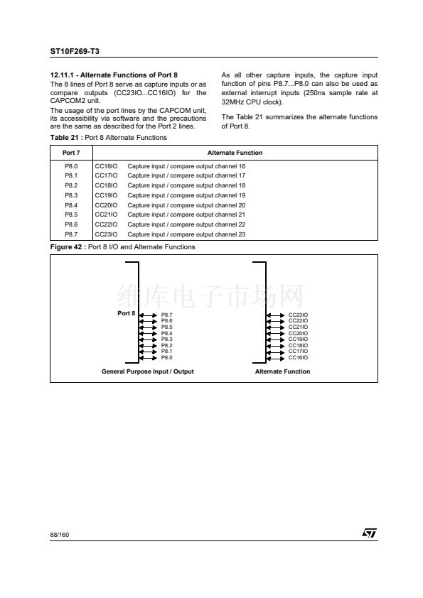
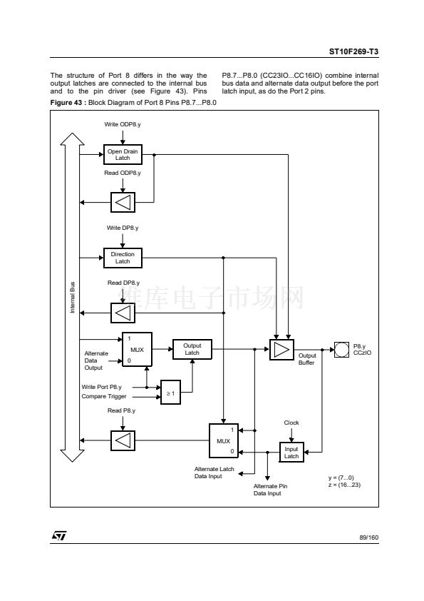
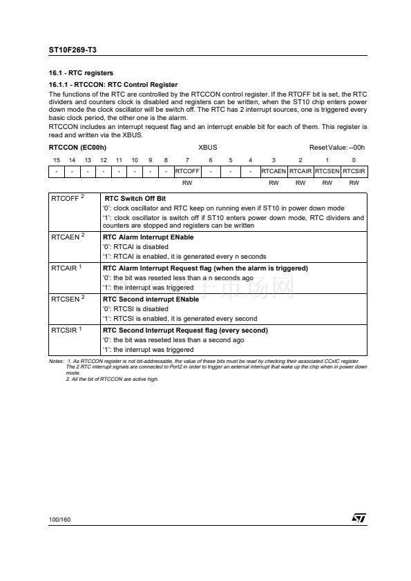
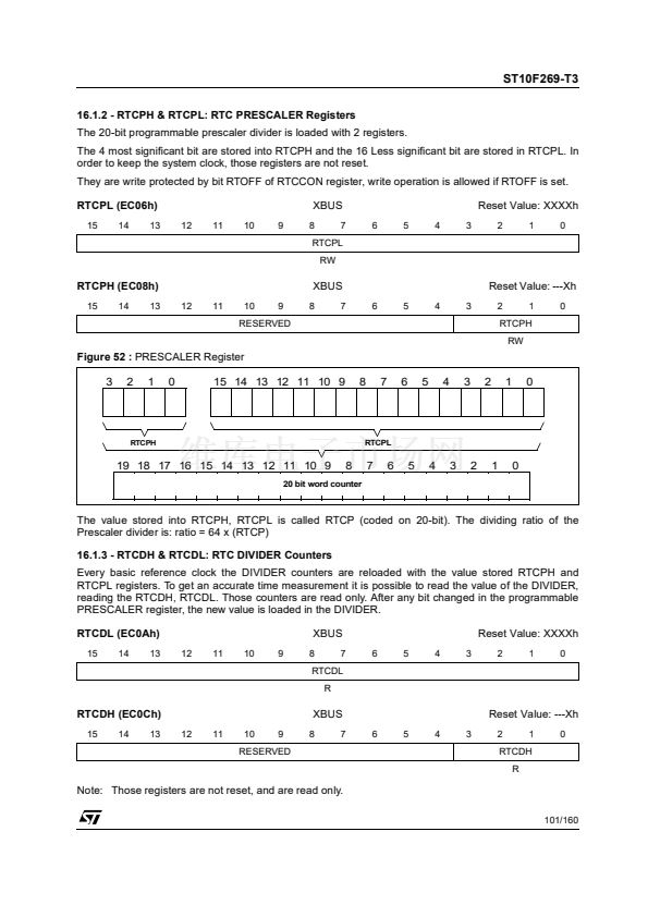
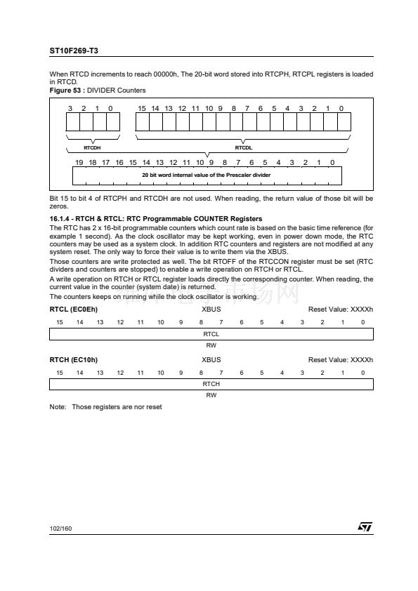
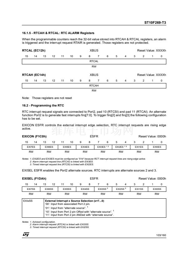
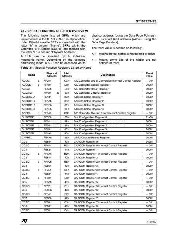
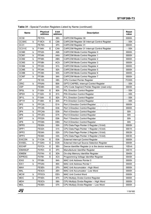
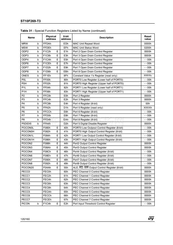
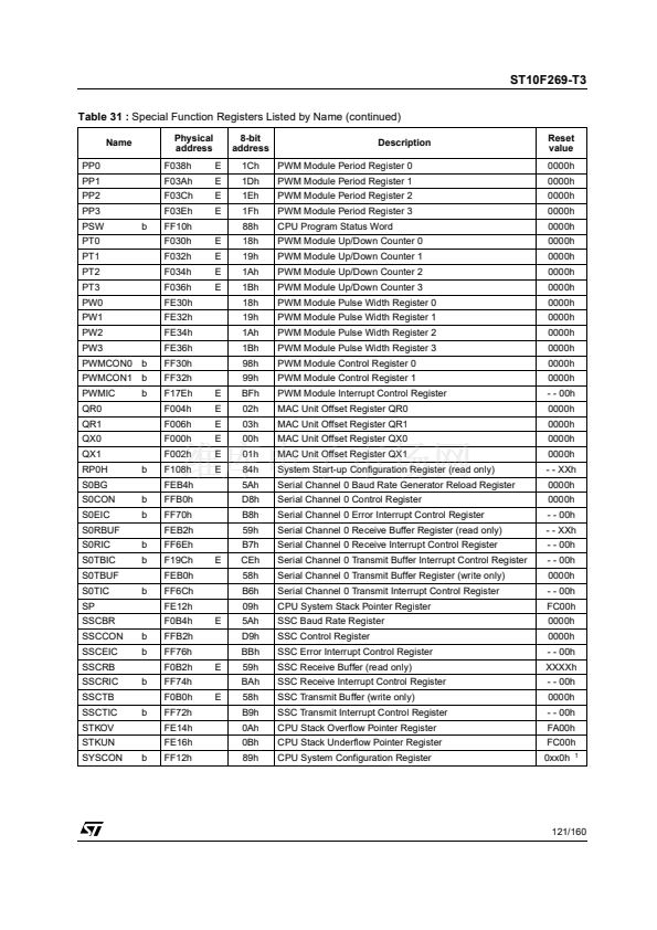
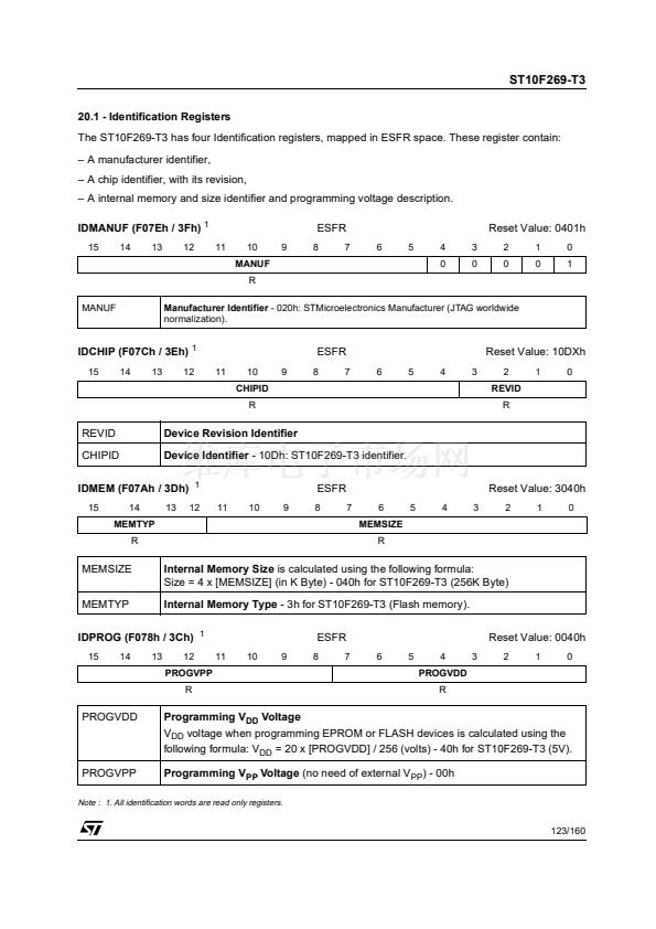
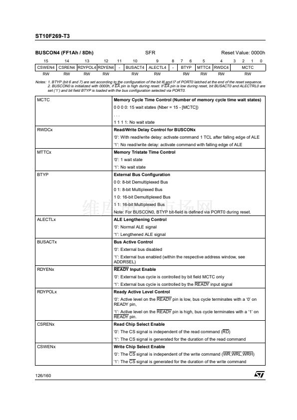
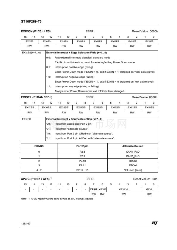
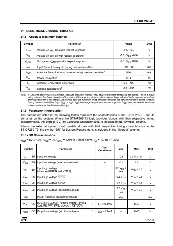
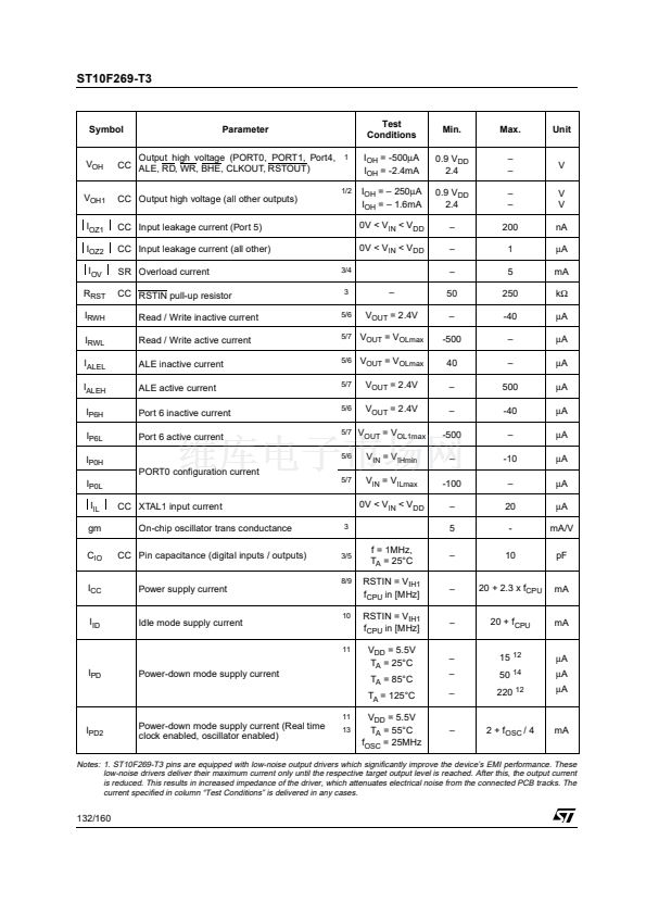
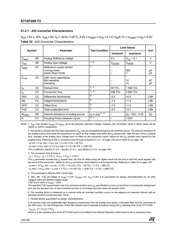
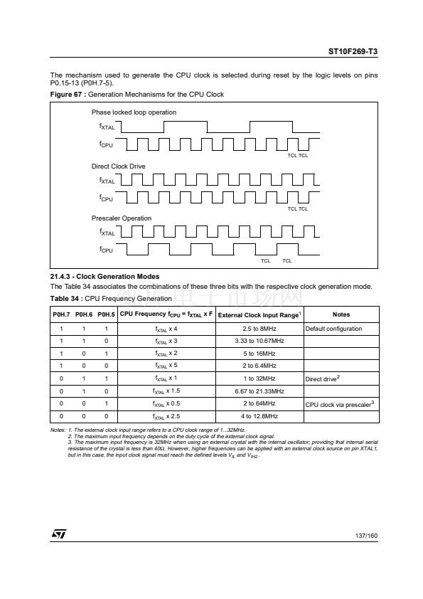
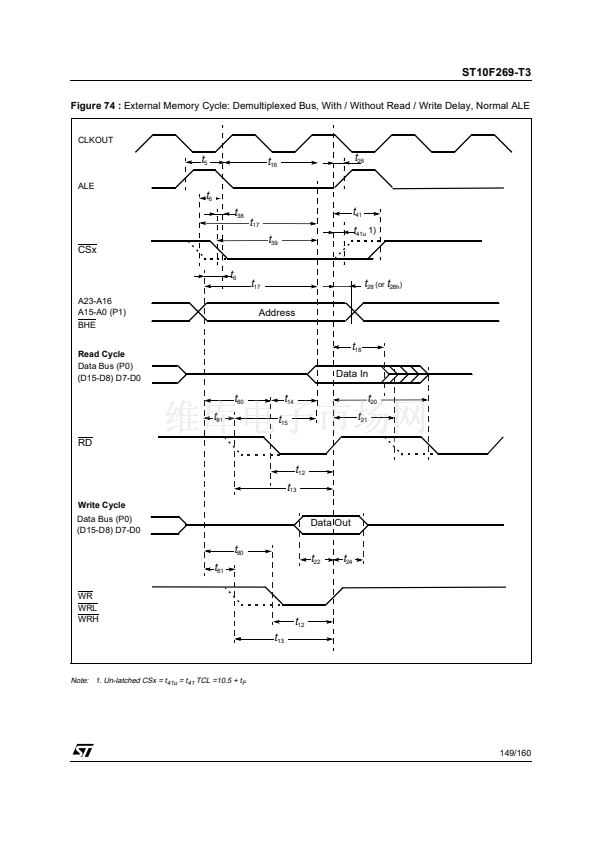
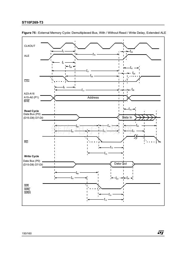
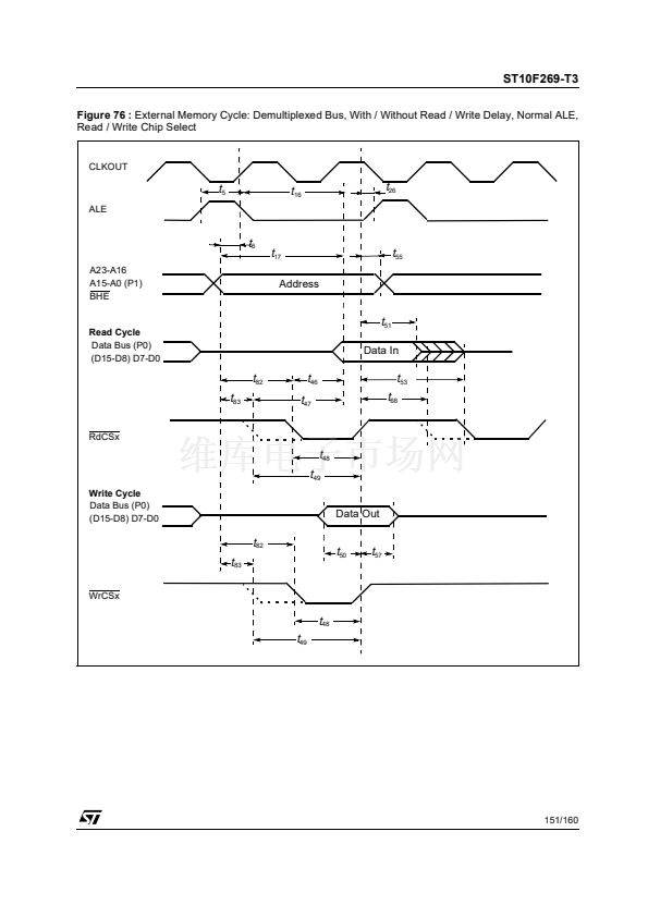
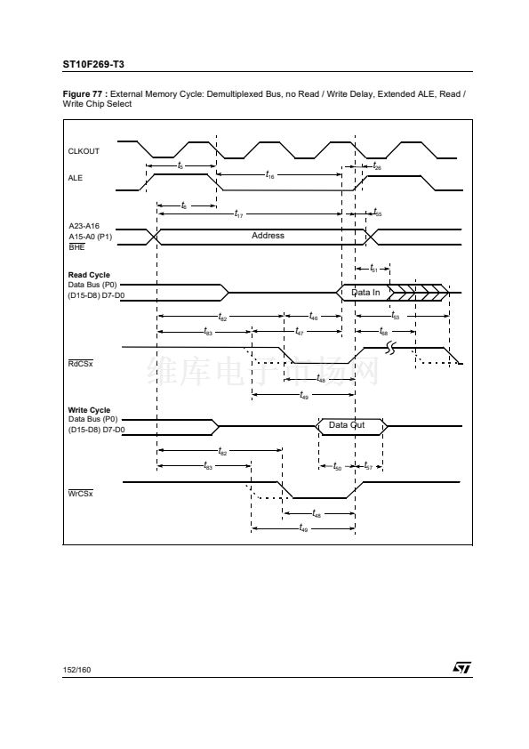
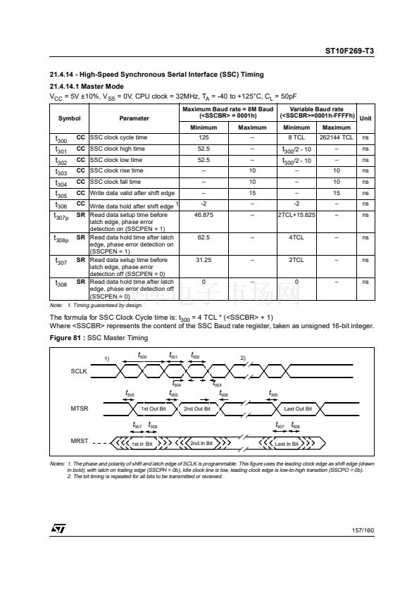
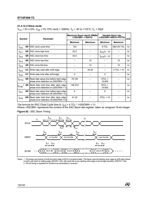
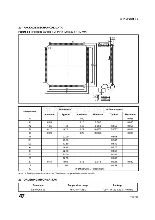
ST10F269-T3
12 - PARALLEL PORTS
12.1 - Introduction
The ST10F269-T3 MCU provides up to 111 I/O
lines with programmable features. These
capabilities bring very flexible adaptation of this
MCU to wide range of applications.
ST10F269-T3 has 9 groups of I/O lines gathered
as following:
鈥?Port 0 is a 2 time 8-bit port named P0L (Low as
less significant Byte) and P0H (high as most sig-
nificant Byte)
鈥?Port 1 is a 2 time 8-bit port named P1L and P1H
鈥?Port 2 is a 16-bit port
鈥?Port 3 is a 15-bit port (P3.14 line is not imple-
mented)
鈥?Port 4 is a 8-bit port
鈥?Port 5 is a 16-bit port input only
鈥?Port 6, Port 7 and Port 8 are 8-bit port
These ports may be used as general purpose
bidirectional input or output, software controlled
with dedicated registers.
For example the output drivers of six of the ports
(2, 3, 4, 6, 7, 8) can be configured (bit-wise) for
push-pull or open drain operation using ODPx
registers.
In addition, the sink and the source capability and
the rise / fall time of the transition of the signal of
some of the push-pull buffers can be programmed
to fit the driving requirements of the application
and to minimize EMI. This feature is implemented
on Port 0, 1, 2, 3, 4, 6, 7 and 8 with the control
registers POCONx. The output drivers capabilities
of ALE, RD, WR control lines are programmable
with the dedicated bits of POCON20 control
register.
The input threshold levels are programmable
(TTL/CMOS) for 5 ports (2, 3, 4, 7, 8). The logic
level of a pin is clocked into the input latch once
per state time, regardless whether the port is
configured for input or output. The threshold is
selected with the PICON register control bits.
A write operation to a port pin configured as an
input causes the value to be written into the port
output latch, while a read operation returns the
latched state of the pin itself. A read-modify-write
operation reads the value of the pin, modifies it,
and writes it back to the output latch.
Writing to a pin configured as an output
(DPx.y=鈥?鈥? causes the output latch and the pin to
have the written value, since the output buffer is
enabled. Reading this pin returns the value of the
output latch. A read-modify-write operation reads
the value of the output latch, modifies it, and
writes it back to the output latch, thus also
modifying the level at the pin.
I/O lines support an alternate function which is
detailed in the following description of each port.
55/160


 1
1
 2
2
 3
3
 4
4
 5
5
 6
6
 7
7
 8
8
 9
9
 10
10
 11
11
 12
12
 13
13
 14
14
 15
15
 16
16
 17
17
 18
18
 19
19
 20
20
 21
21
 22
22
 23
23
 24
24
 25
25
 26
26
 27
27
 28
28
 29
29
 30
30
 31
31
 32
32
 33
33
 34
34
 35
35
 36
36
 37
37
 38
38
 39
39
 40
40
 41
41
 42
42
 43
43
 44
44
 45
45
 46
46
 47
47
 48
48
 49
49
 50
50
 51
51
 52
52
 53
53
 54
54
 55
55
 56
56
 57
57
 58
58
 59
59
 60
60
 61
61
 62
62
 63
63
 64
64
 65
65
 66
66
 67
67
 68
68
 69
69
 70
70
 71
71
 72
72
 73
73
 74
74
 75
75
 76
76
 77
77
 78
78
 79
79
 80
80
 81
81
 82
82
 83
83
 84
84
 85
85
 86
86
 87
87
 88
88
 89
89
 90
90
 91
91
 92
92
 93
93
 94
94
 95
95
 96
96
 97
97
 98
98
 99
99
 100
100
 101
101
 102
102
 103
103
 104
104
 105
105
 106
106
 107
107
 108
108
 109
109
 110
110
 111
111
 112
112
 113
113
 114
114
 115
115
 116
116
 117
117
 118
118
 119
119
 120
120
 121
121
 122
122
 123
123
 124
124
 125
125
 126
126
 127
127
 128
128
 129
129
 130
130
 131
131
 132
132
 133
133
 134
134
 135
135
 136
136
 137
137
 138
138
 139
139
 140
140
 141
141
 142
142
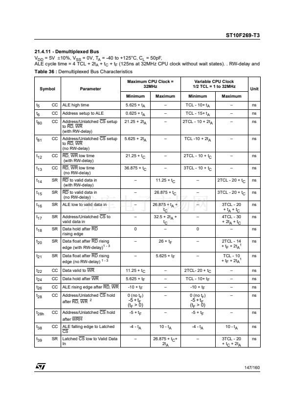
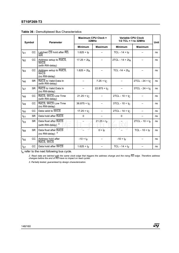
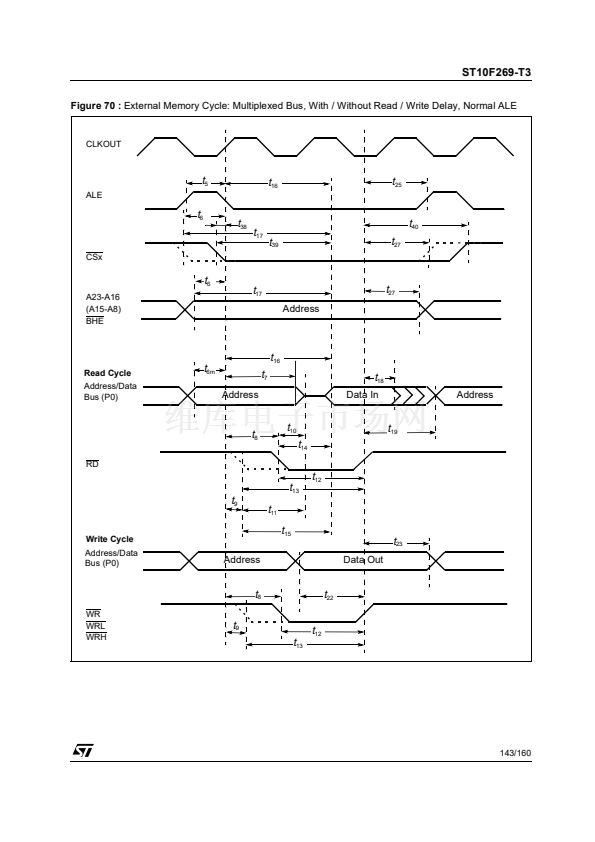 143
143
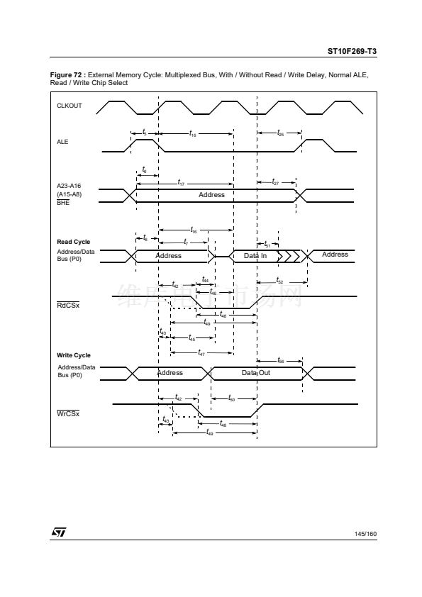
 144
144
 145
145
 146
146
 147
147
 148
148
 149
149
 150
150
 151
151
 152
152
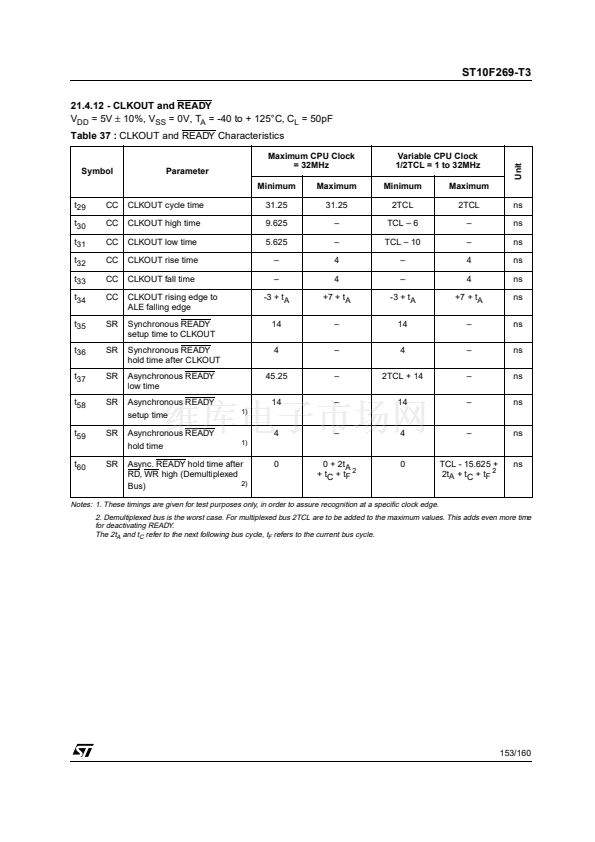 153
153
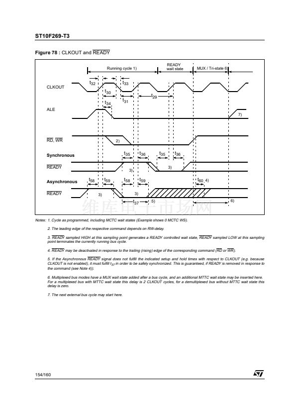 154
154
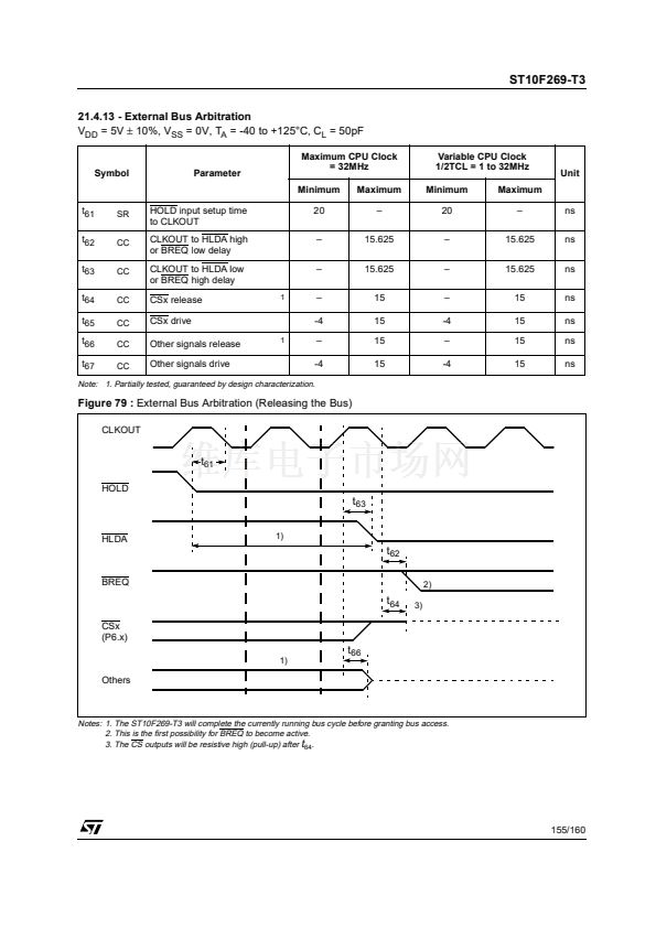 155
155
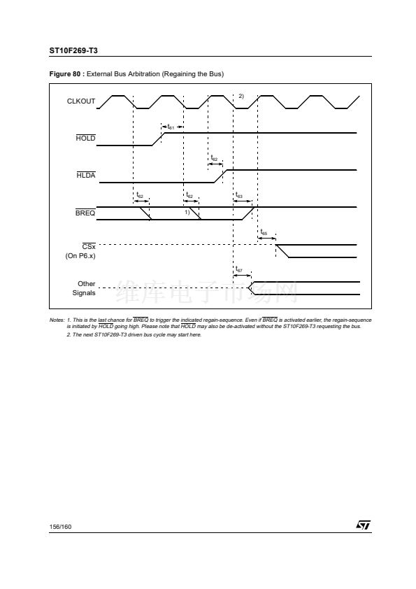 156
156
 157
157
 158
158
 159
159
 160
160
