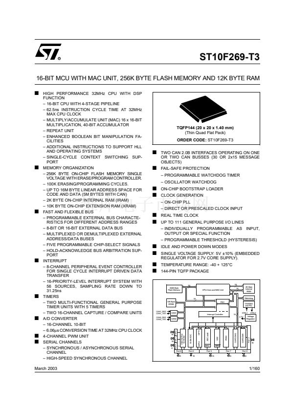
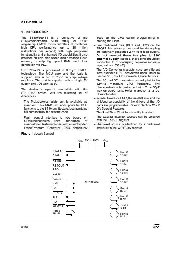
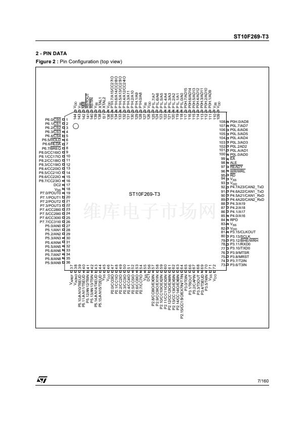
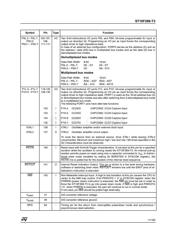
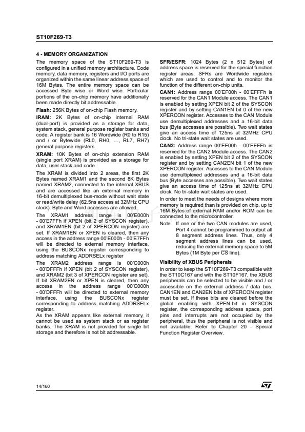
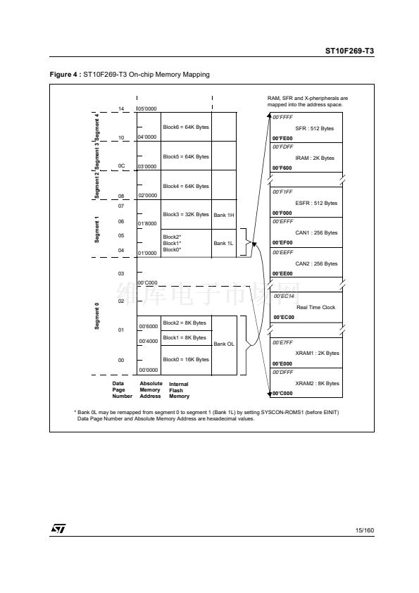
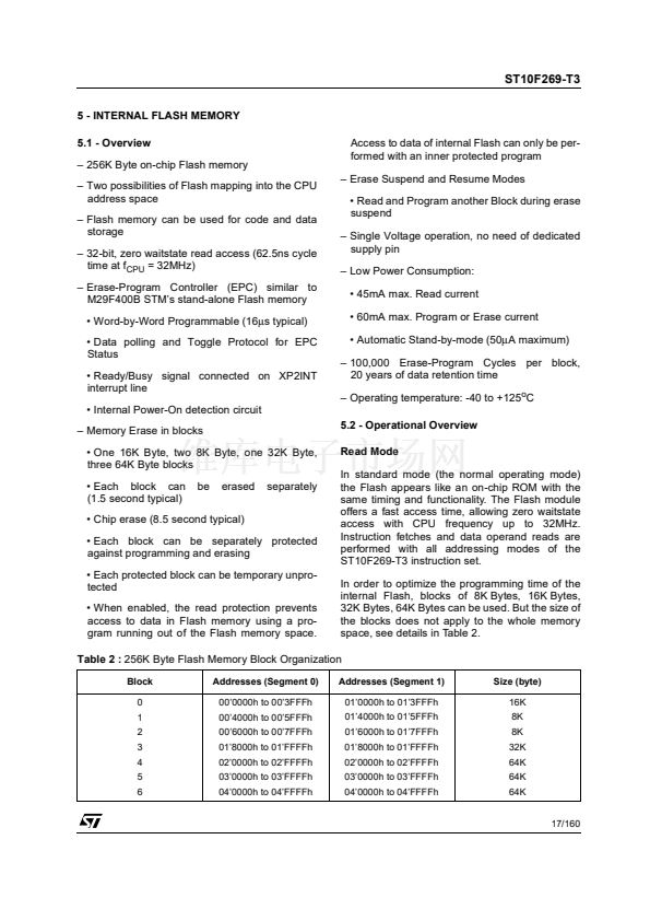
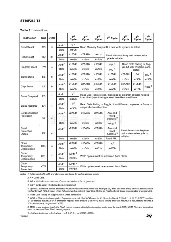
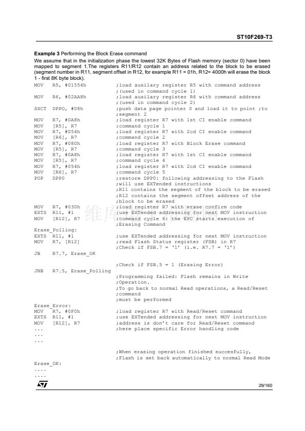
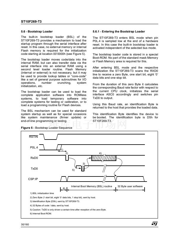
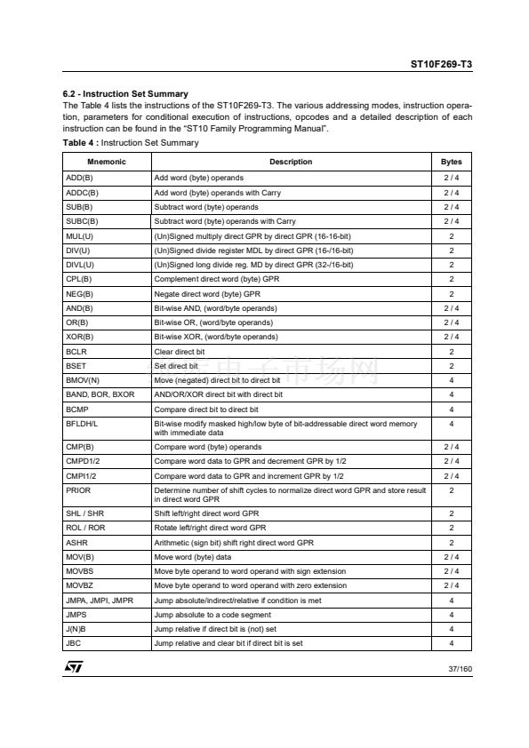
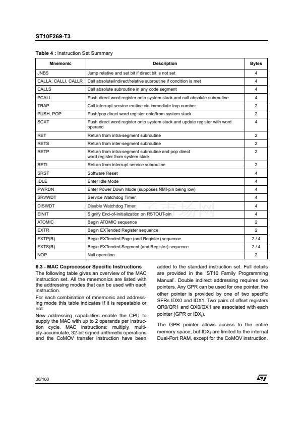
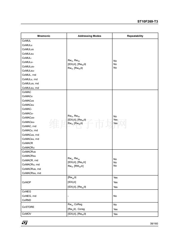
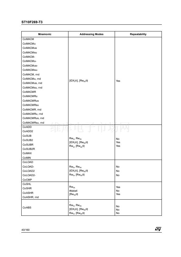
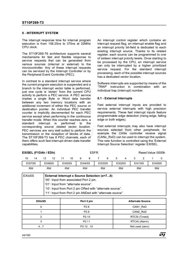
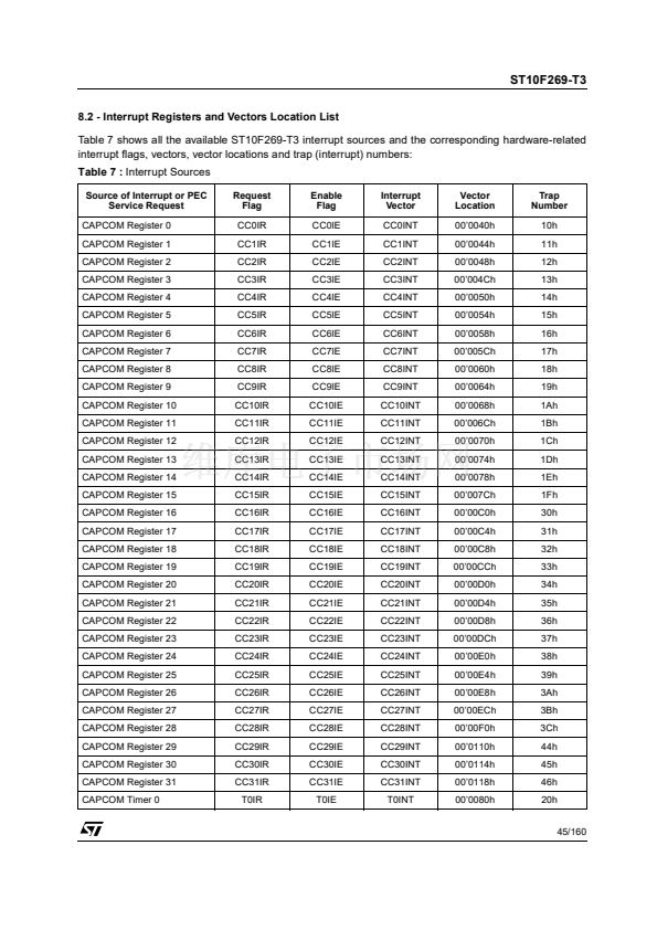
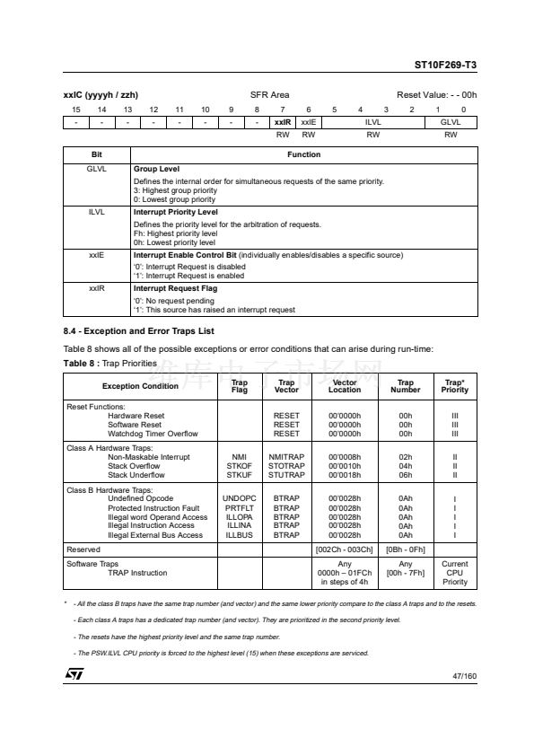
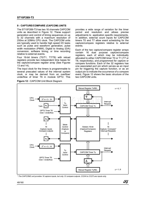
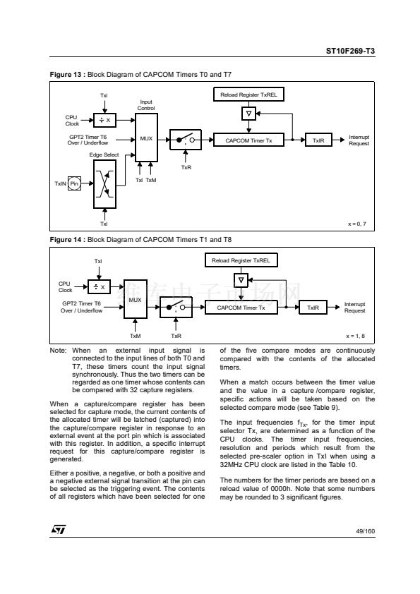
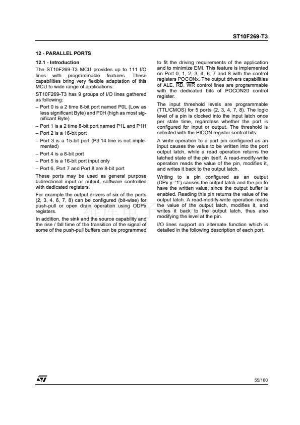
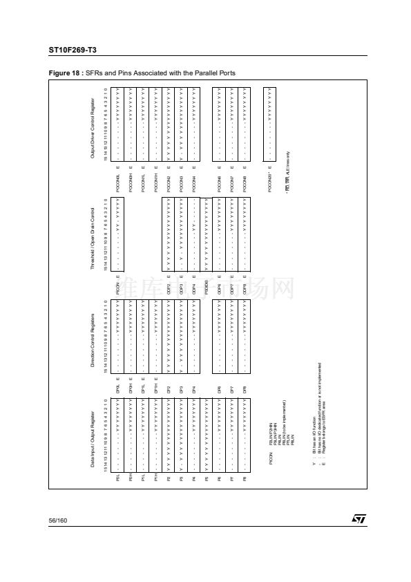
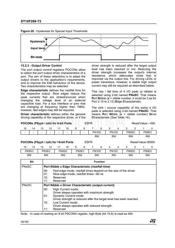
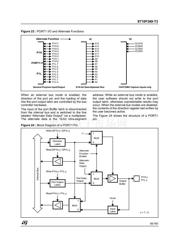
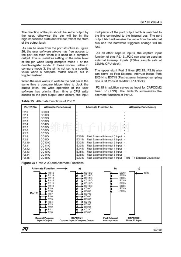
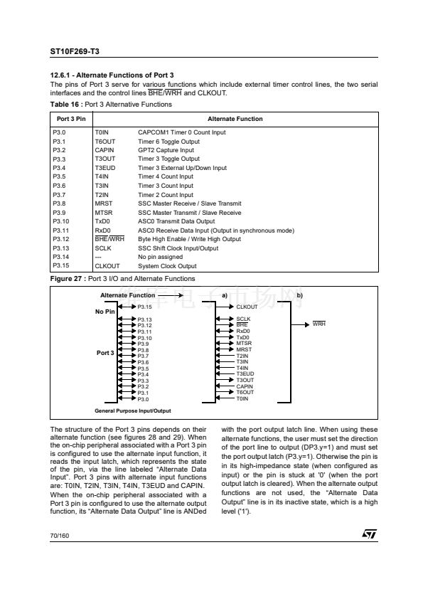
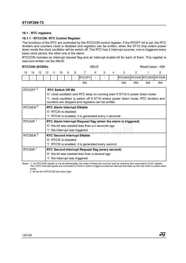
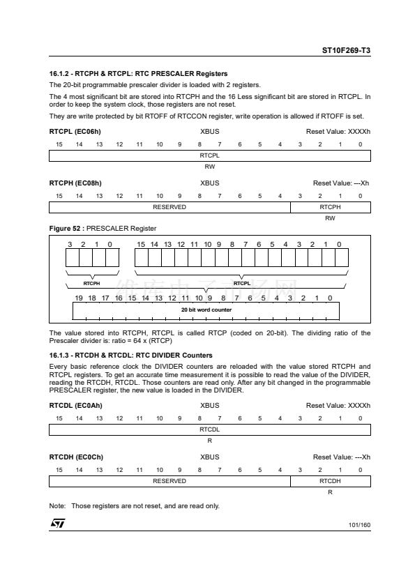
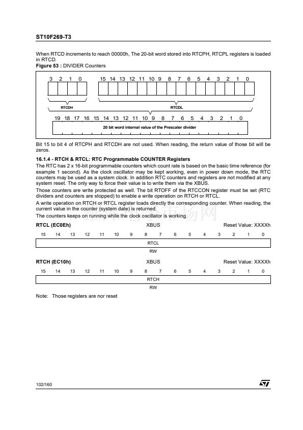
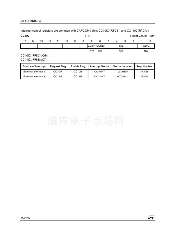
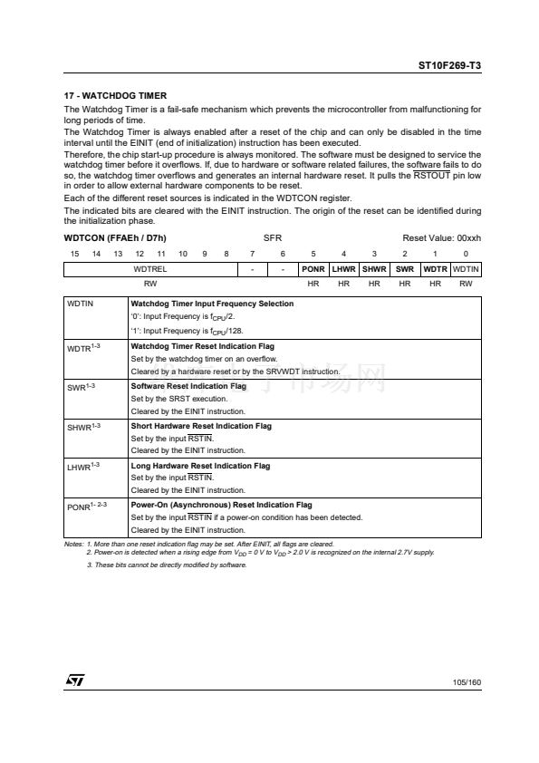
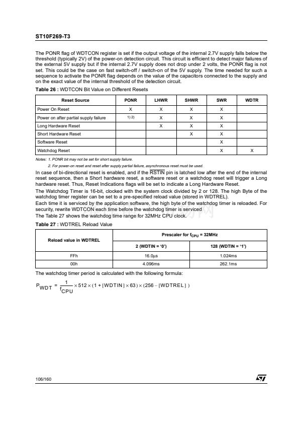
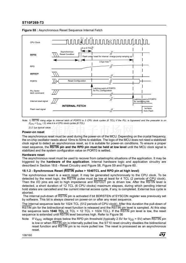
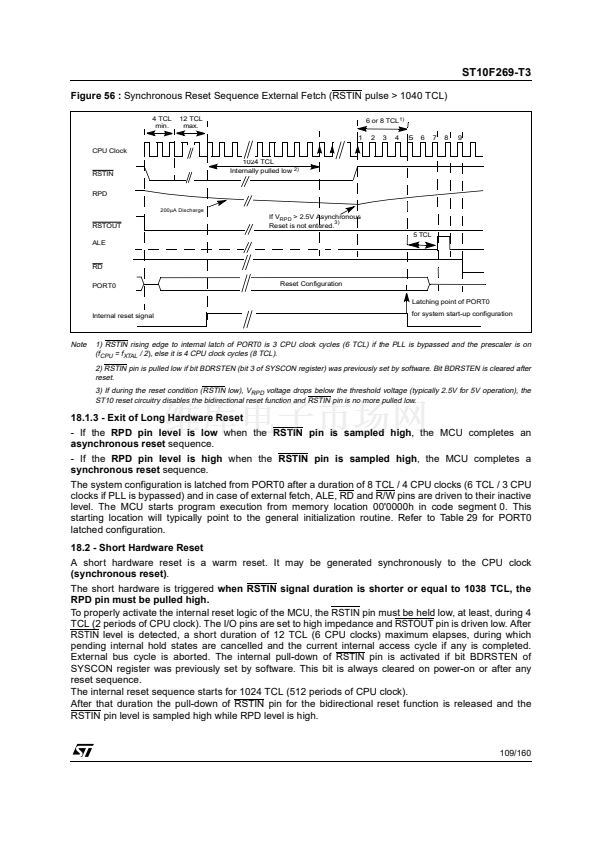
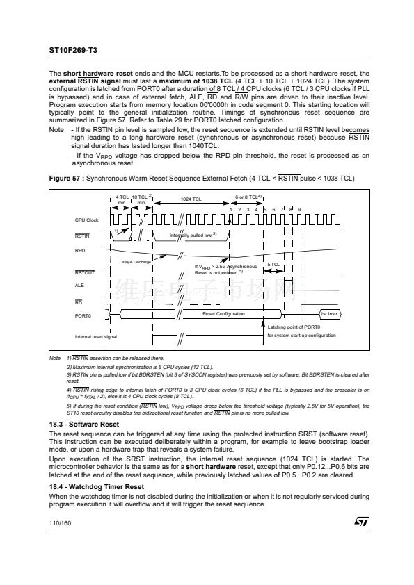
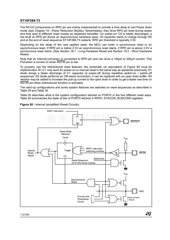
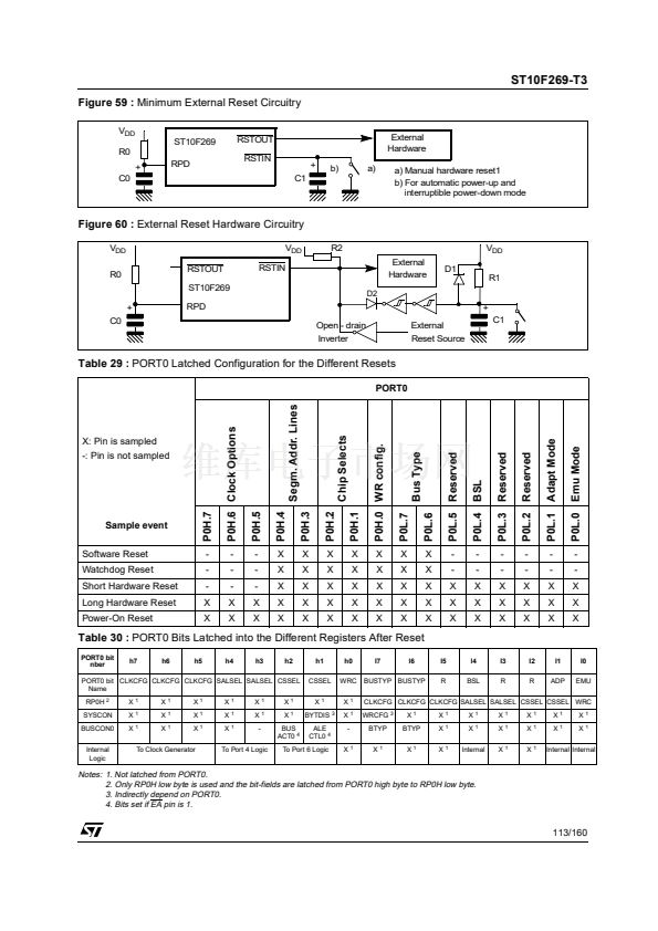
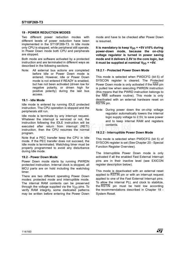
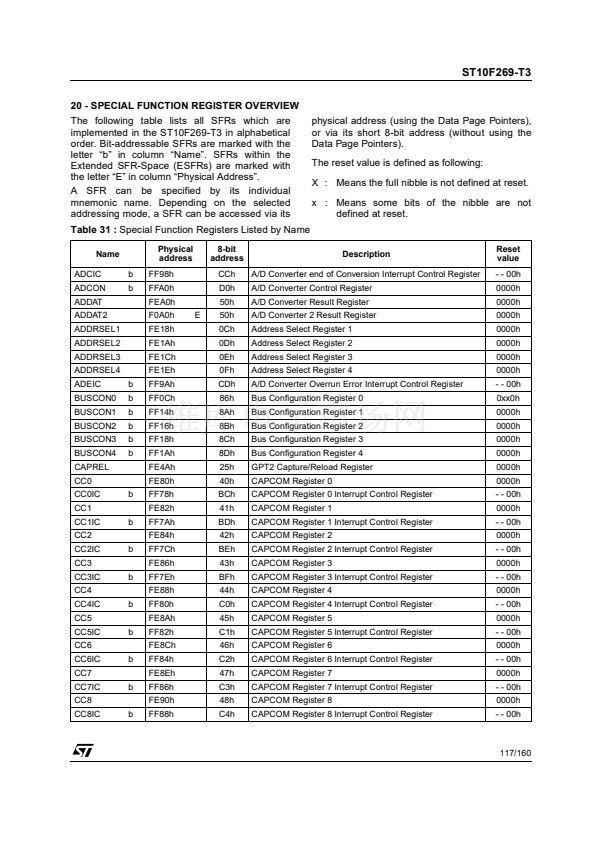
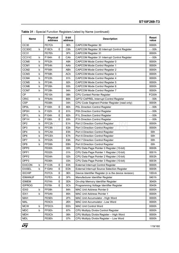
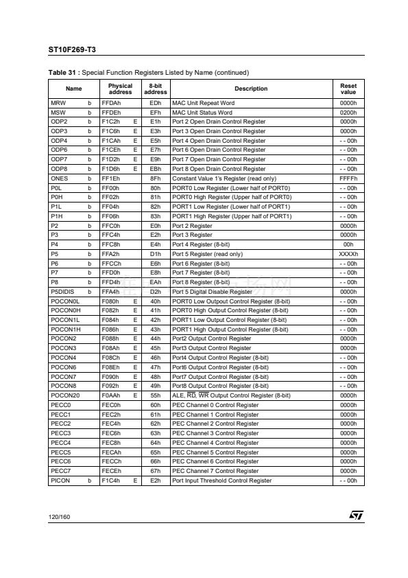
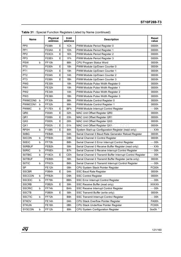
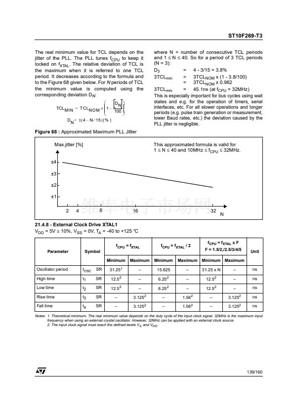
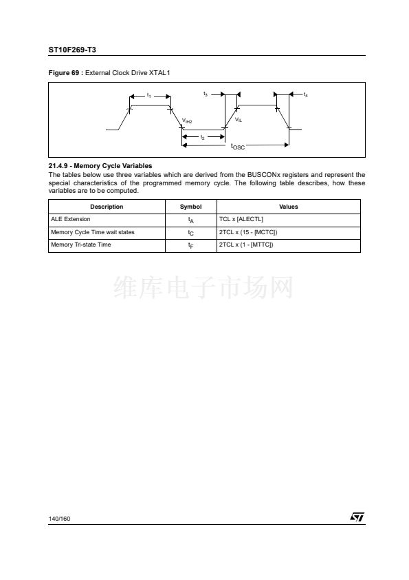
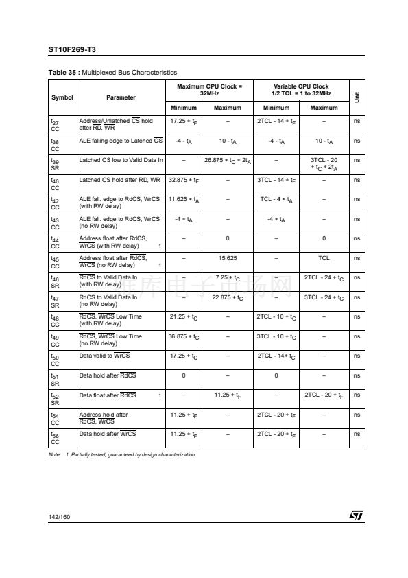
ST10F269-T3
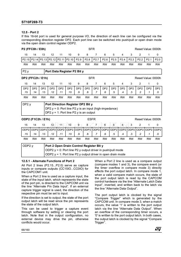
12.5 - Port 2
If this 16-bit port is used for general purpose I/O, the direction of each line can be configured via the
corresponding direction register DP2. Each port line can be switched into push/pull or open drain mode
via the open drain control register ODP2.
P2 (FFC0h / E0h)
15
14
13
12
11
10
9
8
P2.8
RW
SFR
7
P2.7
RW
6
P2.6
RW
5
P2.5
RW
4
P2.4
RW
3
P2.3
RW
Reset Value: 0000h
2
P2.2
RW
1
P2.1
RW
0
P2.0
RW
P2.15 P2.14 P2.13 P2.12 P2.11 P2.10 P2.9
RW
RW
RW
RW
RW
RW
RW
P2.y
Port Data Register P2 Bit y
SFR
12
DP2
.12
RW
11
DP2
.11
RW
10
DP2
.10
RW
9
DP2
.9
RW
8
DP2
.8
RW
7
DP2
.7
RW
6
DP2
.6
RW
5
DP2
.5
RW
4
DP2
.4
RW
3
DP2
.3
RW
DP2 (FFC2h / E1h)
15
DP2
.15
RW
14
DP2
.14
RW
13
DP2
.13
RW
Reset Value: 0000h
2
DP2
.2
RW
1
DP2
.1
RW
0
DP2
.0
RW
DP2.y
Port Direction Register DP2 Bit y
DP2.y = 0: Port line P2.y is an input (high-impedance)
DP2.y = 1: Port line P2.y is an output
ESFR
12
11
10
9
8
7
6
5
4
3
ODP2 (F1C2h / E1h)
15
14
13
Reset Value: 0000h
2
1
0
ODP2 ODP2 ODP2 ODP2 ODP2 ODP2 ODP2 ODP2 ODP2 ODP2 ODP2 ODP2 ODP2 ODP2 ODP2 ODP2
.15
RW
.14
RW
.13
RW
.12
RW
.11
RW
.10
RW
.9
RW
.8
RW
.7
RW
.6
RW
.5
RW
.4
RW
.3
RW
.2
RW
.1
RW
.0
RW
ODP2.y
Port 2 Open Drain Control Register Bit y
ODP2.y = 0: Port line P2.y output driver in push/pull mode
ODP2.y = 1: Port line P2.y output driver in open drain mode
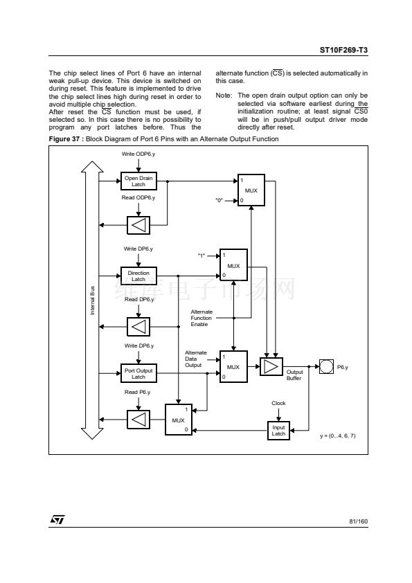
When a Port 2 line is used as a compare output
(compare modes 1 and 3), the compare event (or
the timer overflow in compare mode 3) directly
effects the port output latch. In compare mode 1,
when a valid compare match occurs, the state of
the port output latch is read by the CAPCOM
control hardware via the line 鈥淎lternate Latch Data
Input鈥? inverted, and written back to the latch via
the line 鈥淎lternate Data Output鈥?
The port output latch is clocked by the signal
鈥淐ompare Trigger鈥?which is generated by the
CAPCOM unit. In compare mode 3, when a match
occurs, the value '1' is written to the port output
latch via the line 鈥淎lternate Data Output鈥? When
an overflow of the corresponding timer occurs, a
'0' is written to the port output latch. In both cases,
the output latch is clocked by the signal 鈥淐ompare
Trigger鈥?
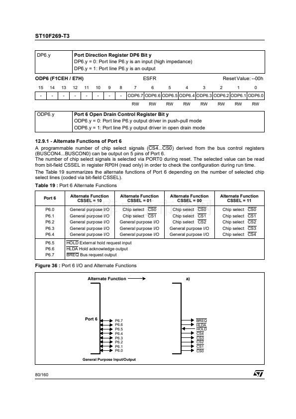
12.5.1 - Alternate Functions of Port 2
All Port 2 lines (P2.15...P2.0) serve as capture
inputs or compare outputs (CC15IO...CC0IO) for
the CAPCOM1 unit.
When a Port 2 line is used as a capture input, the
state of the input latch, which represents the state
of the port pin, is directed to the CAPCOM unit via
the line 鈥淎lternate Pin Data Input鈥? If an external
capture trigger signal is used, the direction of the
respective pin must be set to input.
If the direction is set to output, the state of the port
output latch will be read since the pin represents
the state of the output latch.
This can be used to trigger a capture event
through software by setting or clearing the port
latch. Note that in the output configuration, no
external device may drive the pin, otherwise
conflicts would occur.
66/160


 1
1
 2
2
 3
3
 4
4
 5
5
 6
6
 7
7
 8
8
 9
9
 10
10
 11
11
 12
12
 13
13
 14
14
 15
15
 16
16
 17
17
 18
18
 19
19
 20
20
 21
21
 22
22
 23
23
 24
24
 25
25
 26
26
 27
27
 28
28
 29
29
 30
30
 31
31
 32
32
 33
33
 34
34
 35
35
 36
36
 37
37
 38
38
 39
39
 40
40
 41
41
 42
42
 43
43
 44
44
 45
45
 46
46
 47
47
 48
48
 49
49
 50
50
 51
51
 52
52
 53
53
 54
54
 55
55
 56
56
 57
57
 58
58
 59
59
 60
60
 61
61
 62
62
 63
63
 64
64
 65
65
 66
66
 67
67
 68
68
 69
69
 70
70
 71
71
 72
72
 73
73
 74
74
 75
75
 76
76
 77
77
 78
78
 79
79
 80
80
 81
81
 82
82
 83
83
 84
84
 85
85
 86
86
 87
87
 88
88
 89
89
 90
90
 91
91
 92
92
 93
93
 94
94
 95
95
 96
96
 97
97
 98
98
 99
99
 100
100
 101
101
 102
102
 103
103
 104
104
 105
105
 106
106
 107
107
 108
108
 109
109
 110
110
 111
111
 112
112
 113
113
 114
114
 115
115
 116
116
 117
117
 118
118
 119
119
 120
120
 121
121
 122
122
 123
123
 124
124
 125
125
 126
126
 127
127
 128
128
 129
129
 130
130
 131
131
 132
132
 133
133
 134
134
 135
135
 136
136
 137
137
 138
138
 139
139
 140
140
 141
141
 142
142
 143
143
 144
144
 145
145
 146
146
 147
147
 148
148
 149
149
 150
150
 151
151
 152
152
 153
153
 154
154
 155
155
 156
156
 157
157
 158
158
 159
159
 160
160
