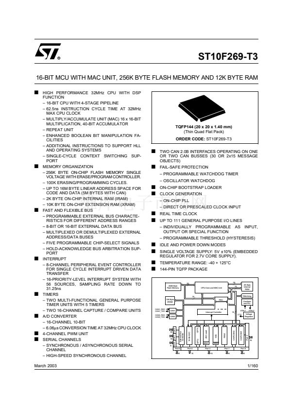
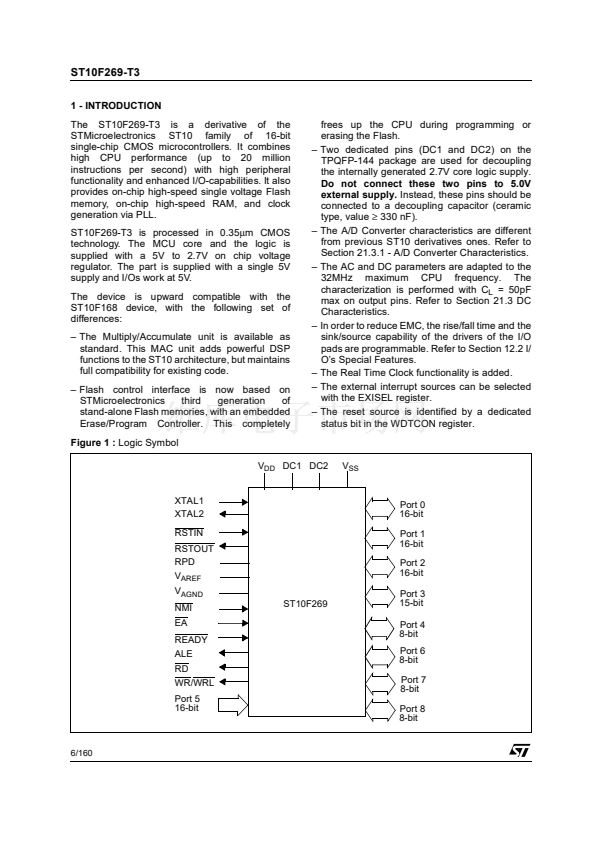
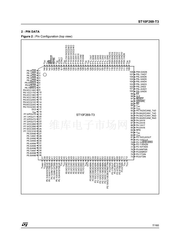
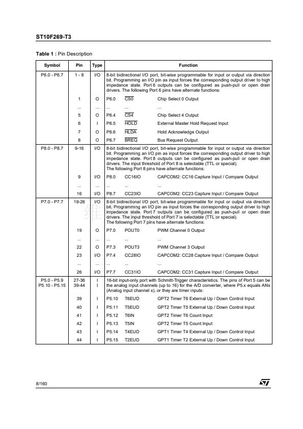
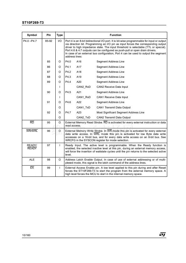
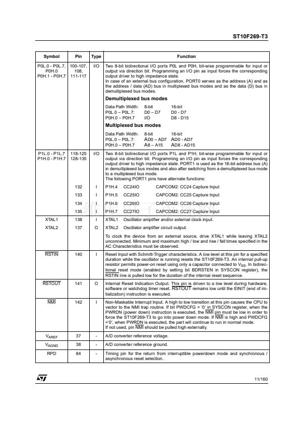
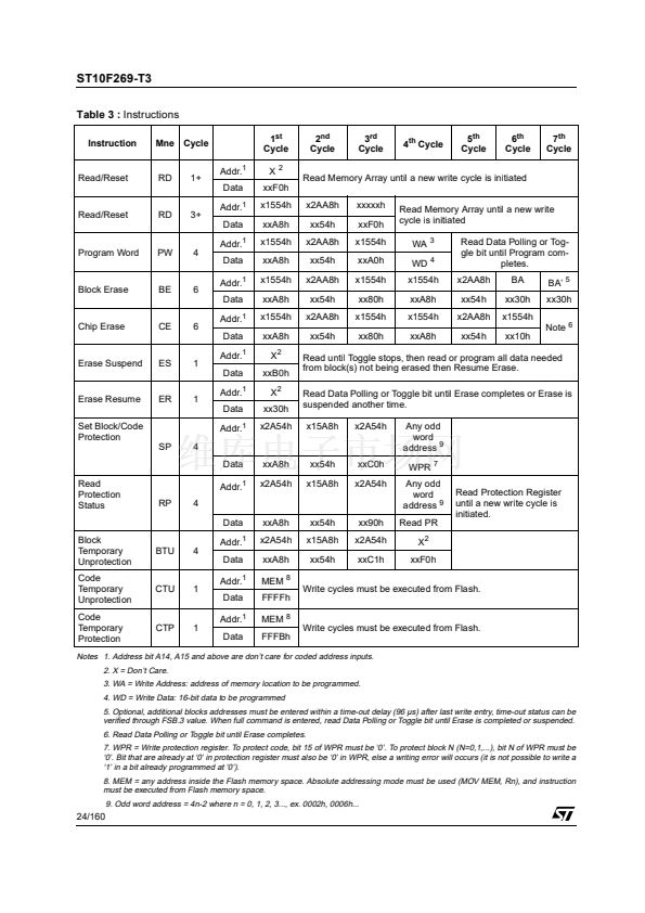
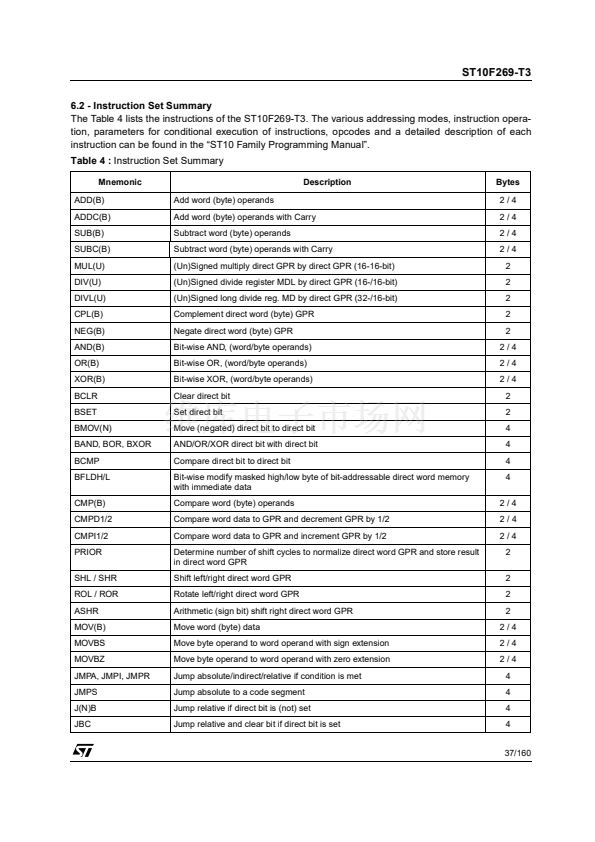
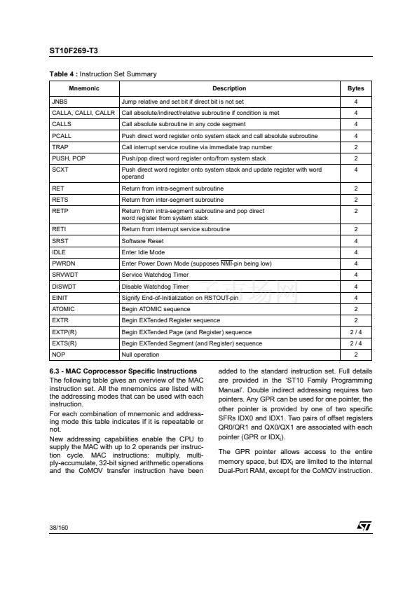
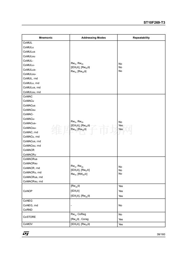
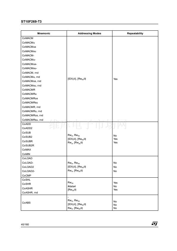
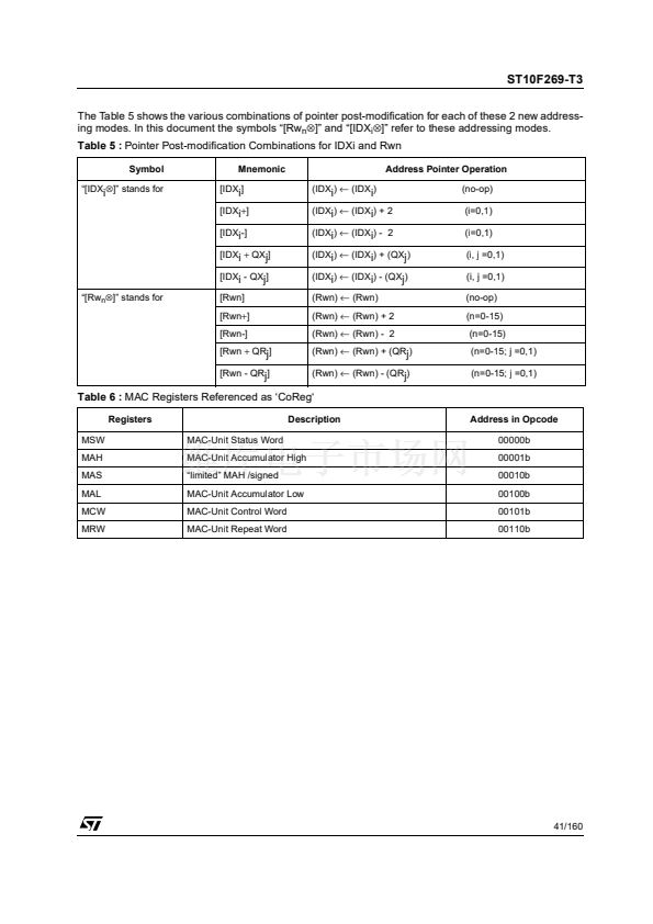
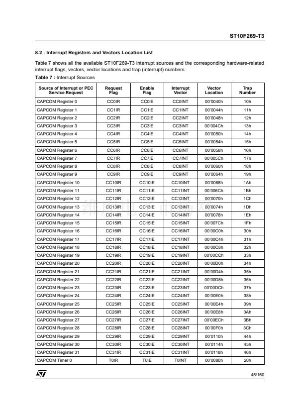
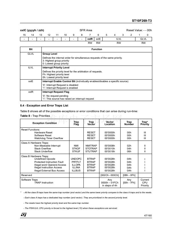
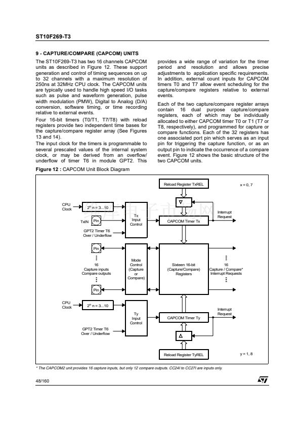
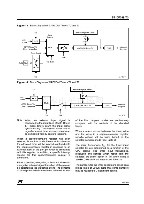
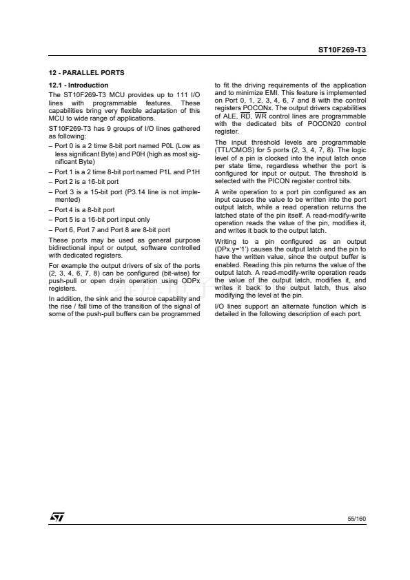
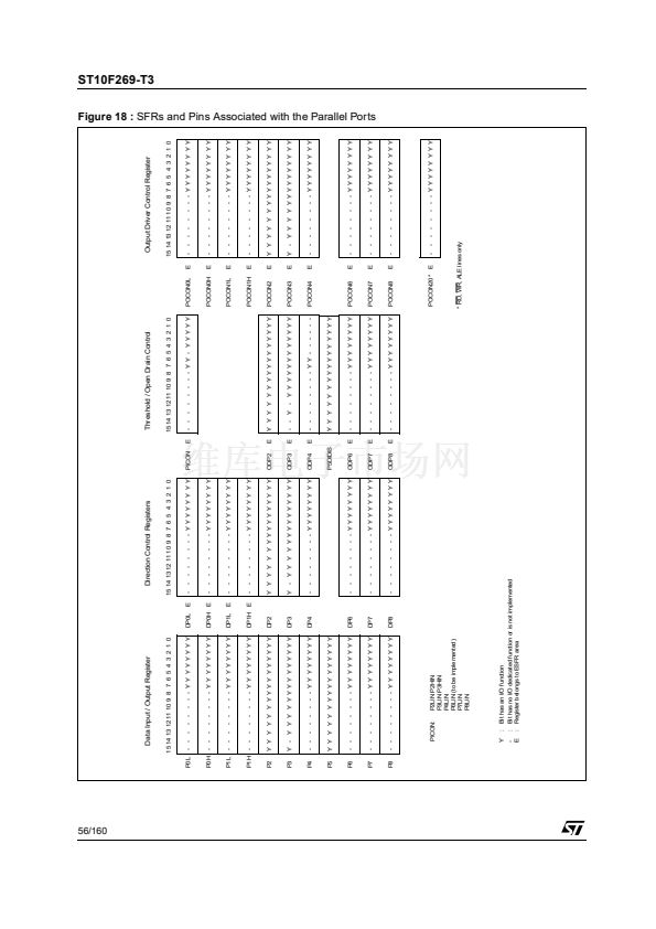
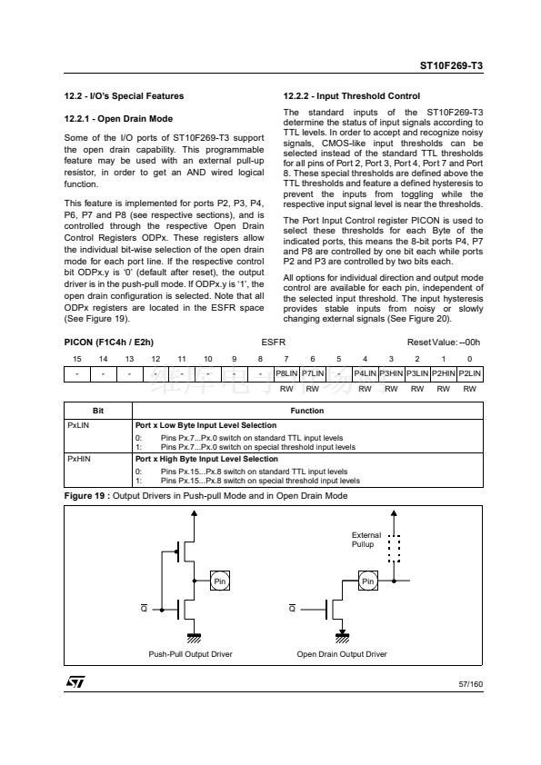
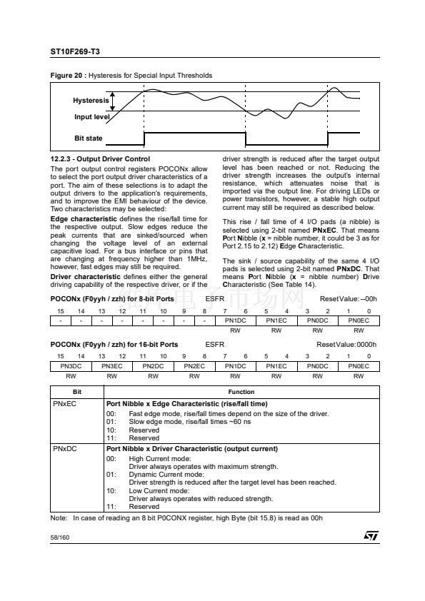
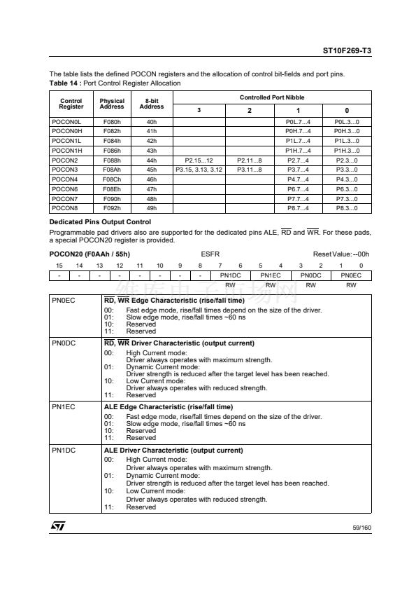
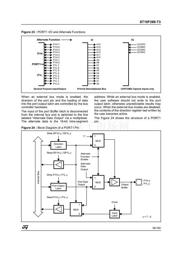
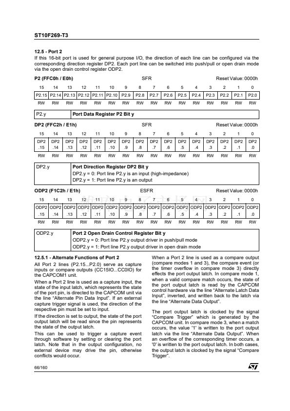
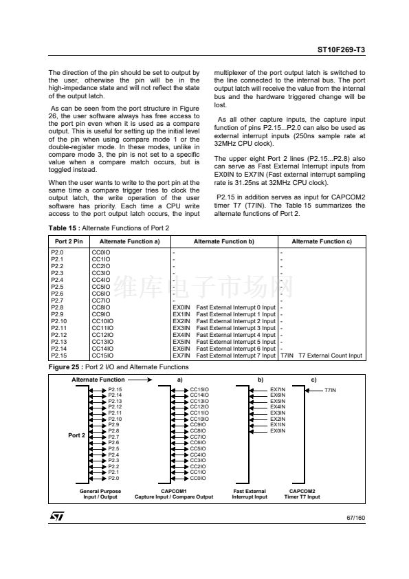
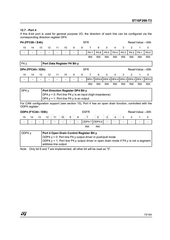
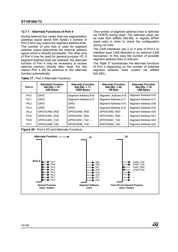
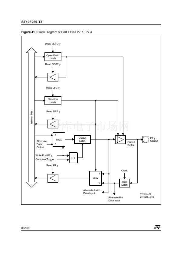
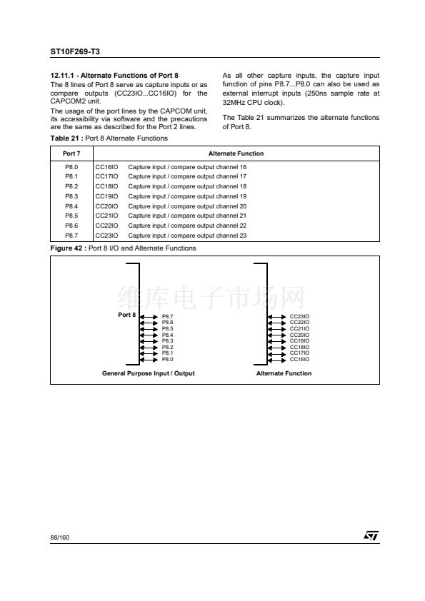
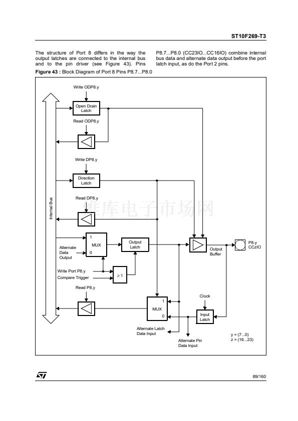
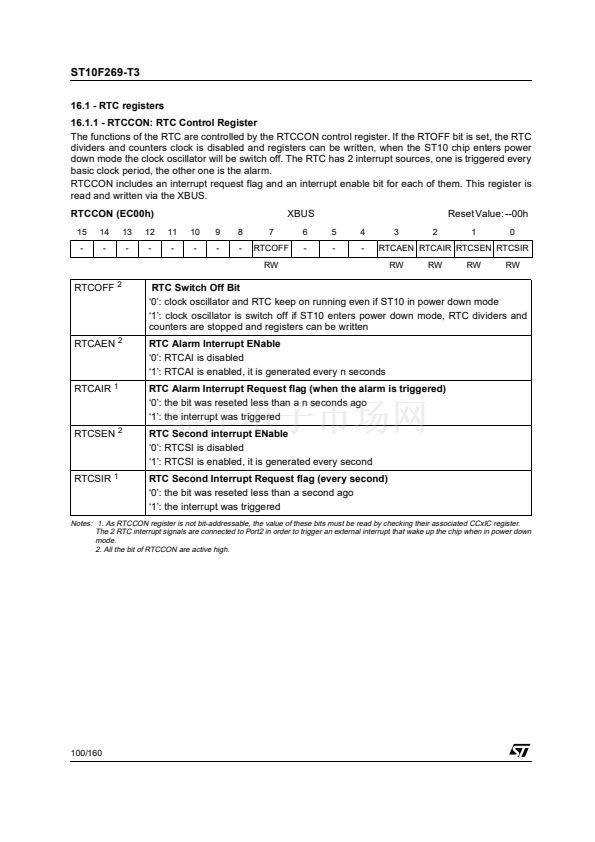
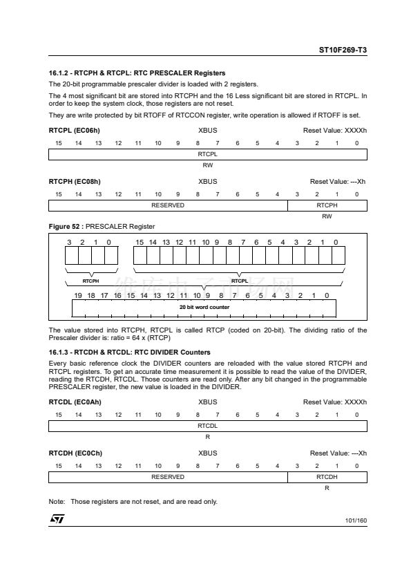
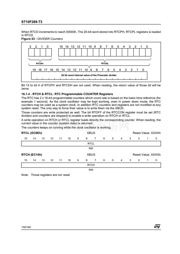
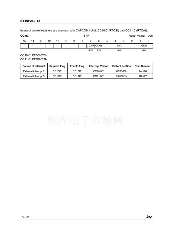
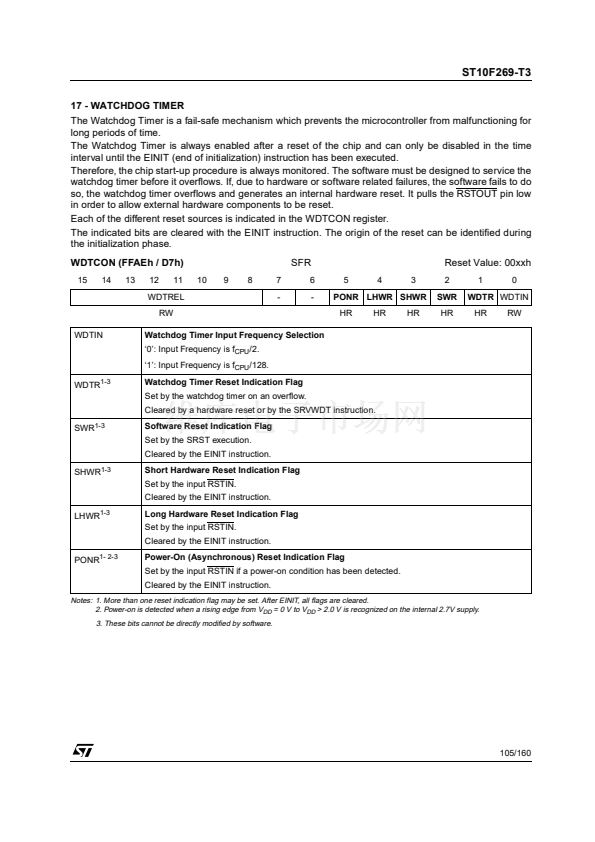
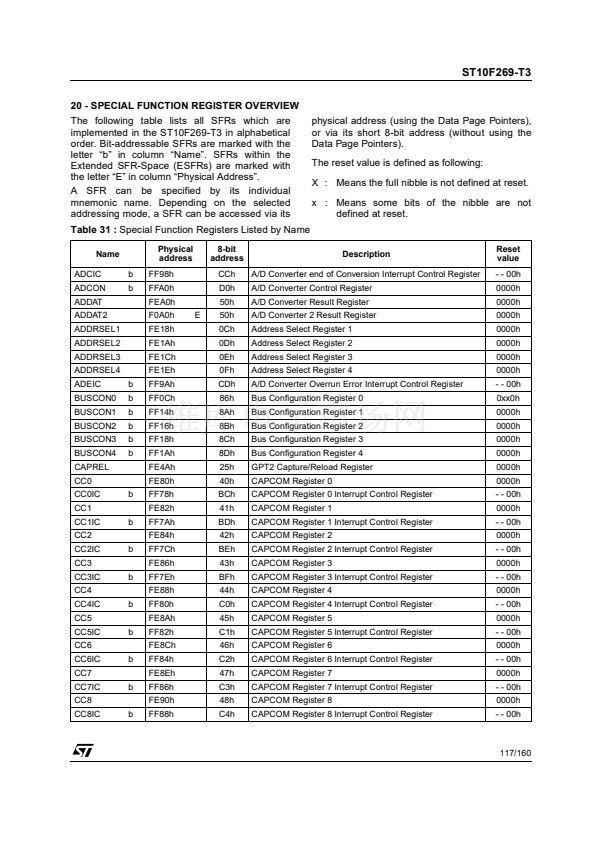
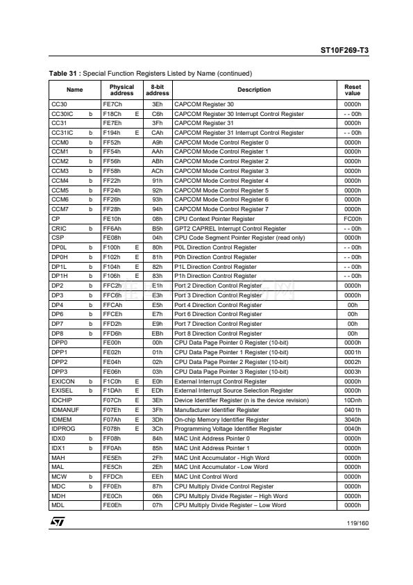
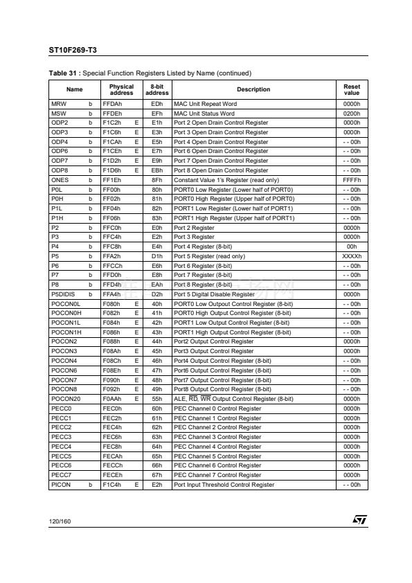
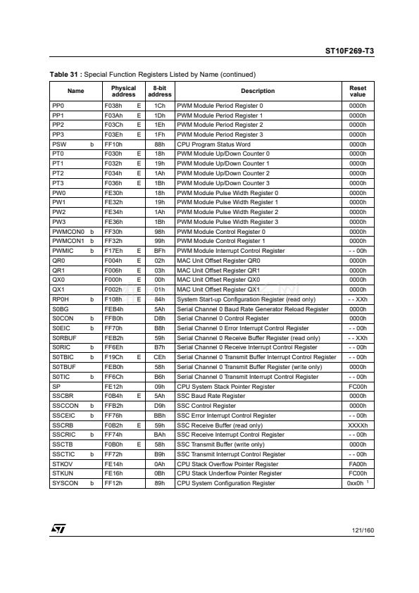
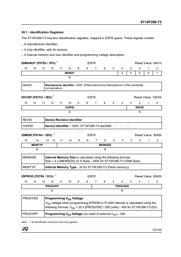
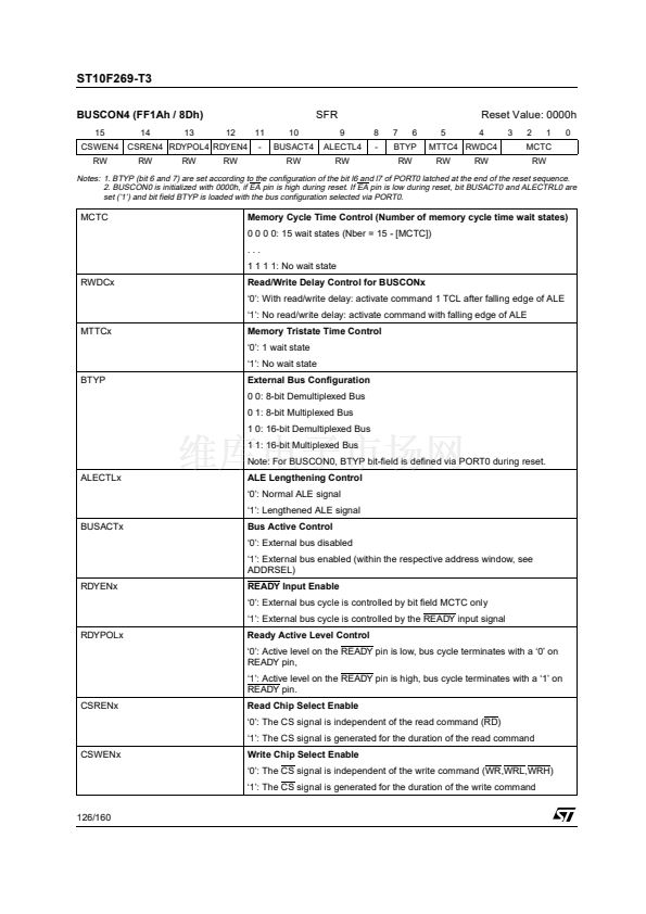
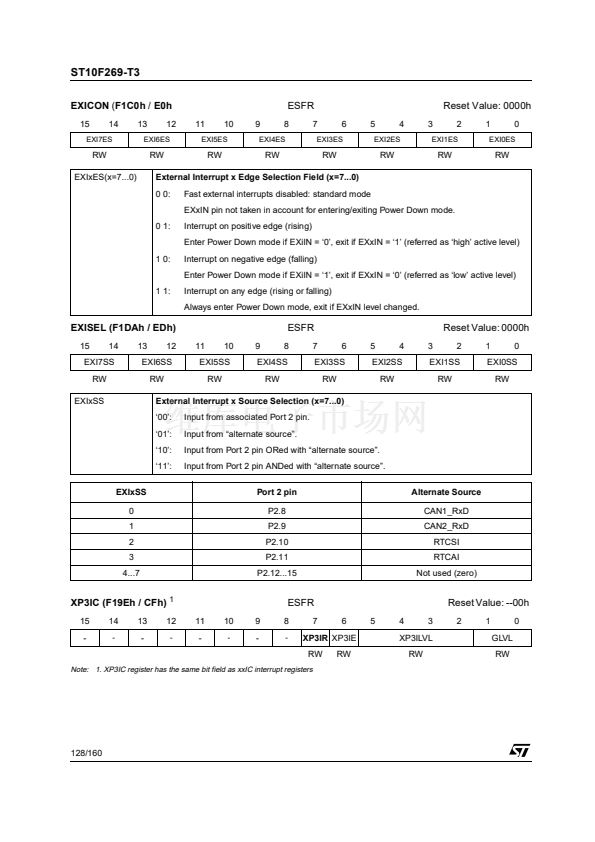
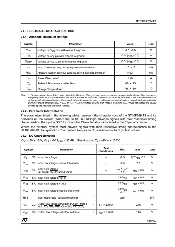
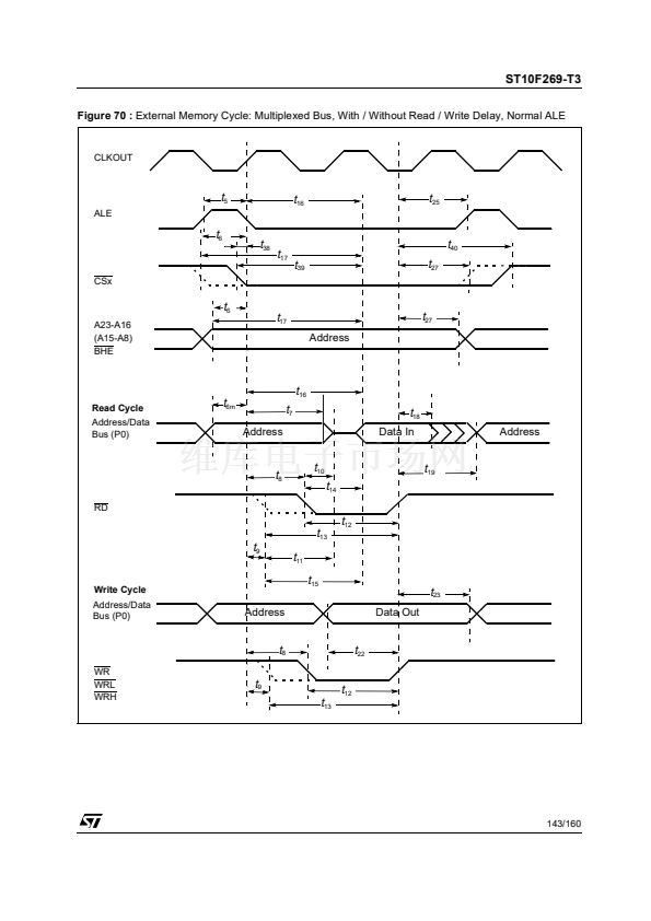
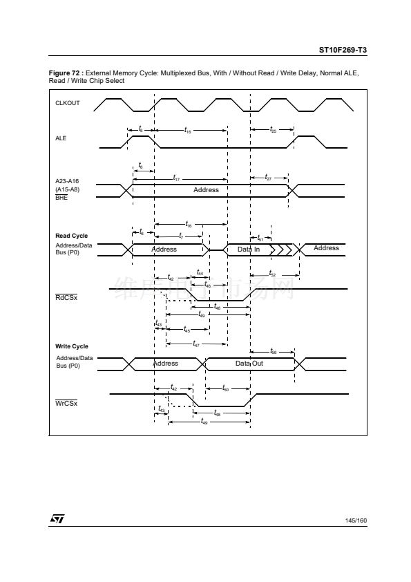
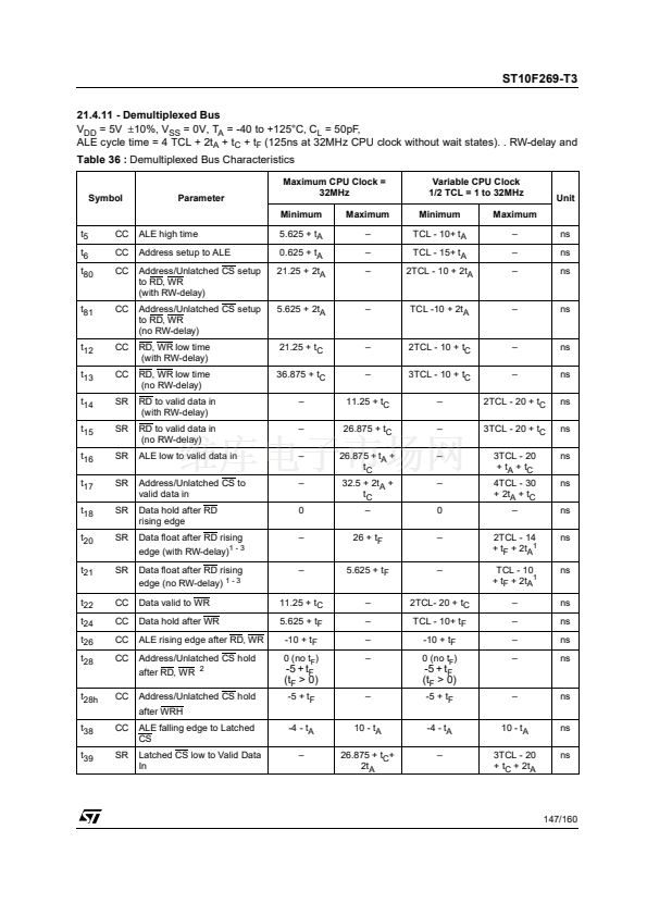
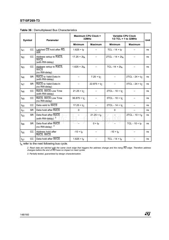
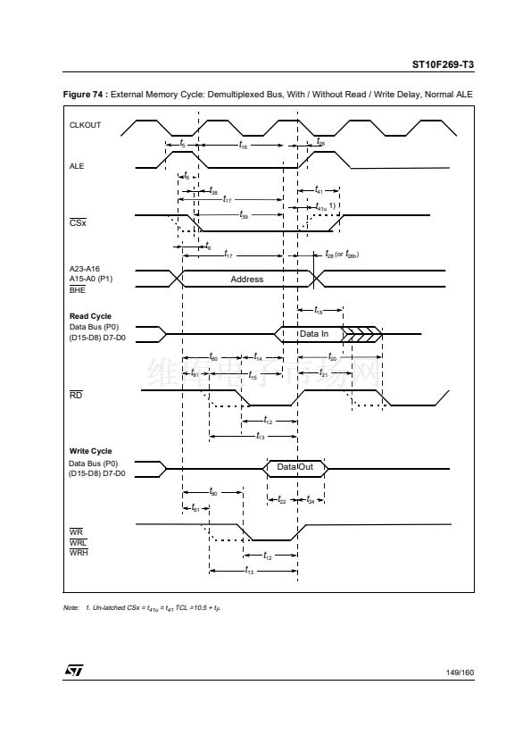
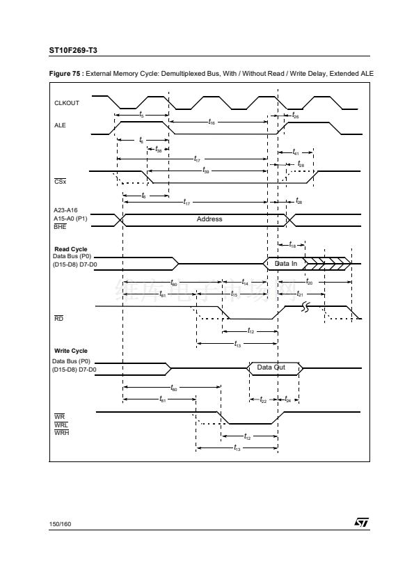
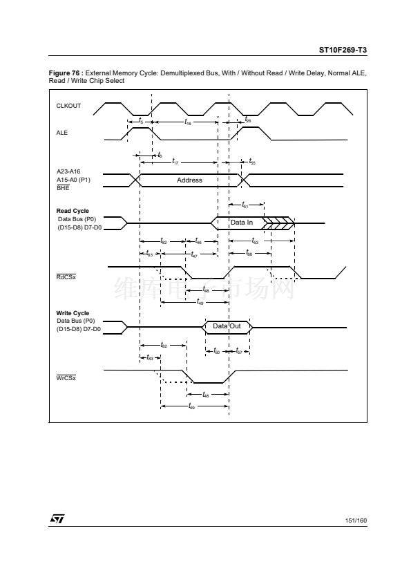
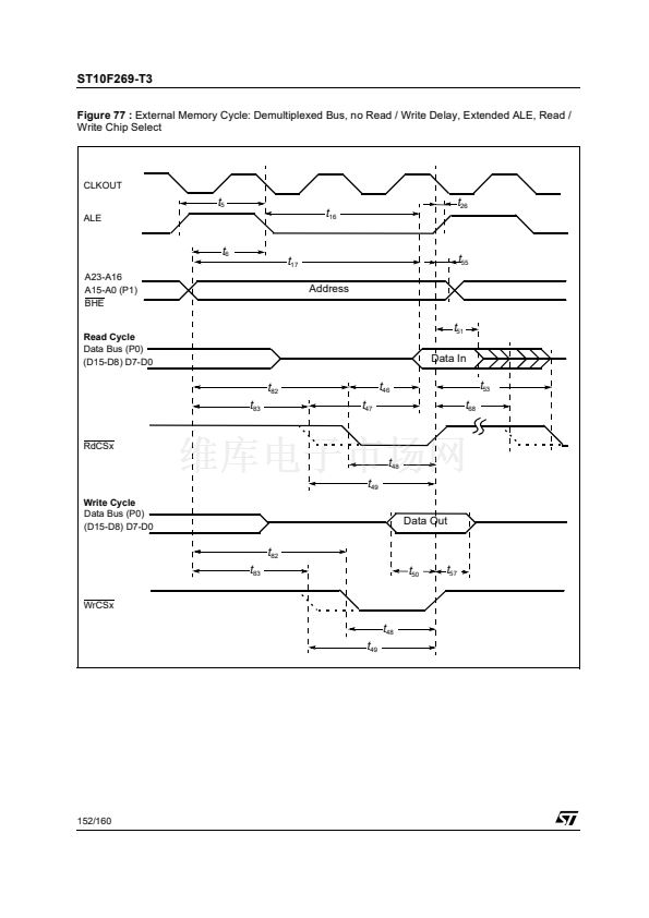
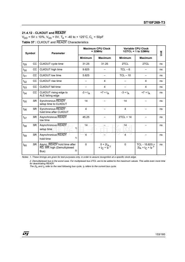
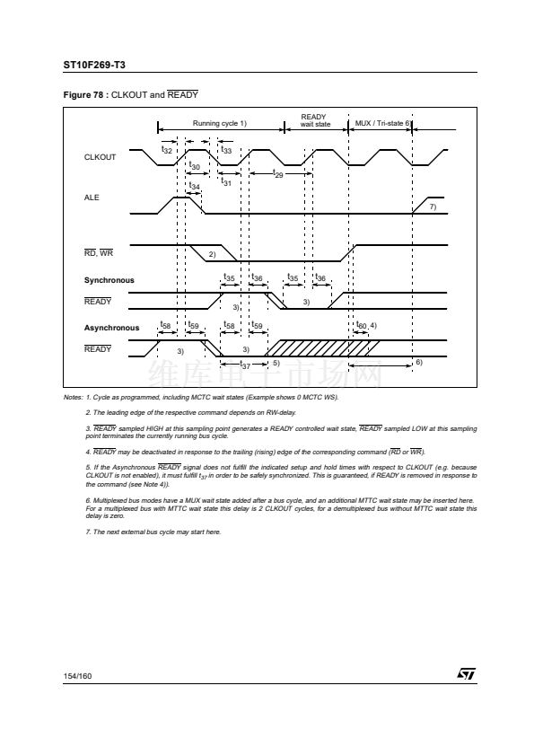
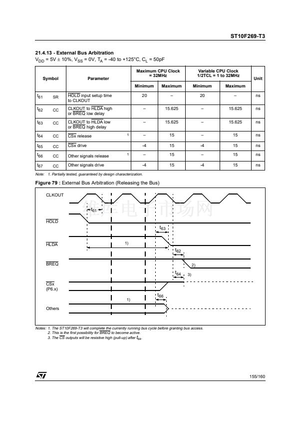
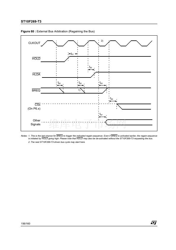
ST10F269-T3
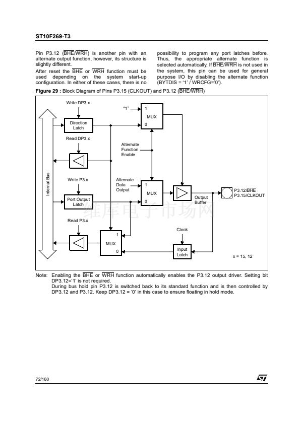
Pin P3.12 (BHE/WRH) is another pin with an
alternate output function, however, its structure is
slightly different.
After reset the BHE or WRH function must be
used depending on the system start-up
configuration. In either of these cases, there is no
possibility to program any port latches before.
Thus, the appropriate alternate function is
selected automatically. If BHE/WRH is not used in
the system, this pin can be used for general
purpose I/O by disabling the alternate function
(BYTDIS = 鈥?鈥?/ WRCFG=鈥?鈥?.
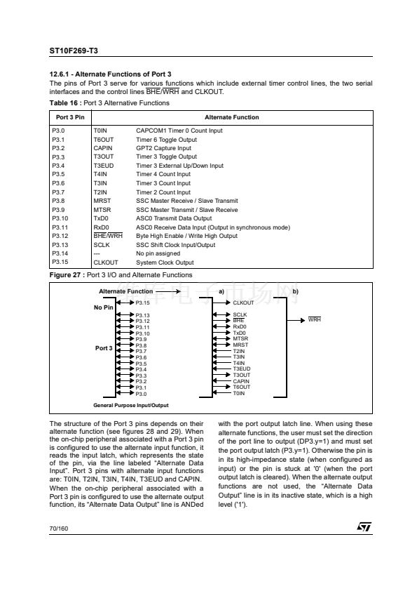
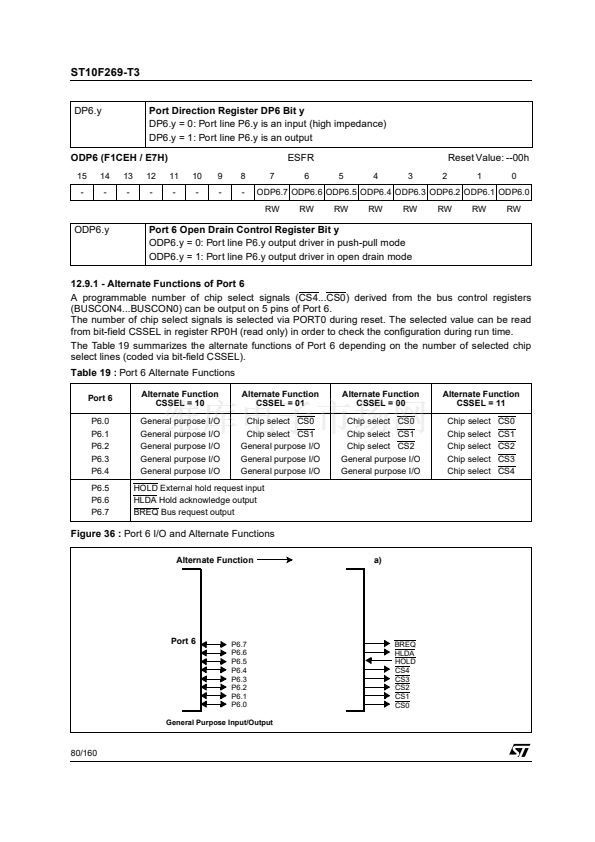
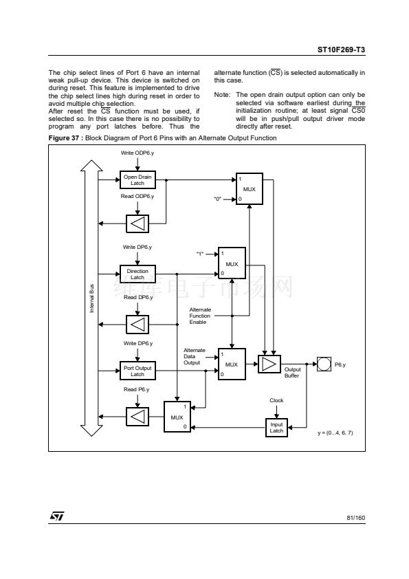
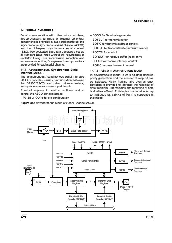
Figure 29 :
Block Diagram of Pins P3.15 (CLKOUT) and P3.12 (BHE/WRH)
Write DP3.x
鈥?鈥?/div>
Direction
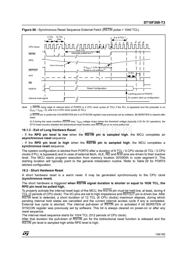
Latch
Read DP3.x
Alternate
Function
Enable
1
MUX
0
Internal Bus
Write P3.x
Alternate
Data
Output
1
MUX
0
Output
Buffer
P3.12/BHE
P3.15/CLKOUT
Port Output
Latch
Read P3.x
Clock
1
MUX
0
Input
Latch
x = 15, 12
Note: Enabling the BHE or WRH function automatically enables the P3.12 output driver. Setting bit
DP3.12=鈥?鈥?is not required.
During bus hold pin P3.12 is switched back to its standard function and is then controlled by
DP3.12 and P3.12. Keep DP3.12 = 鈥?鈥?in this case to ensure floating in hold mode.
72/160


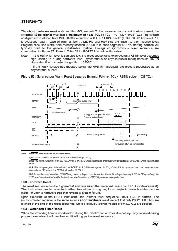
 1
1
 2
2
 3
3
 4
4
 5
5
 6
6
 7
7
 8
8
 9
9
 10
10
 11
11
 12
12
 13
13
 14
14
 15
15
 16
16
 17
17
 18
18
 19
19
 20
20
 21
21
 22
22
 23
23
 24
24
 25
25
 26
26
 27
27
 28
28
 29
29
 30
30
 31
31
 32
32
 33
33
 34
34
 35
35
 36
36
 37
37
 38
38
 39
39
 40
40
 41
41
 42
42
 43
43
 44
44
 45
45
 46
46
 47
47
 48
48
 49
49
 50
50
 51
51
 52
52
 53
53
 54
54
 55
55
 56
56
 57
57
 58
58
 59
59
 60
60
 61
61
 62
62
 63
63
 64
64
 65
65
 66
66
 67
67
 68
68
 69
69
 70
70
 71
71
 72
72
 73
73
 74
74
 75
75
 76
76
 77
77
 78
78
 79
79
 80
80
 81
81
 82
82
 83
83
 84
84
 85
85
 86
86
 87
87
 88
88
 89
89
 90
90
 91
91
 92
92
 93
93
 94
94
 95
95
 96
96
 97
97
 98
98
 99
99
 100
100
 101
101
 102
102
 103
103
 104
104
 105
105
 106
106
 107
107
 108
108
 109
109
 110
110
 111
111
 112
112
 113
113
 114
114
 115
115
 116
116
 117
117
 118
118
 119
119
 120
120
 121
121
 122
122
 123
123
 124
124
 125
125
 126
126
 127
127
 128
128
 129
129
 130
130
 131
131
 132
132
 133
133
 134
134
 135
135
 136
136
 137
137
 138
138
 139
139
 140
140
 141
141
 142
142
 143
143
 144
144
 145
145
 146
146
 147
147
 148
148
 149
149
 150
150
 151
151
 152
152
 153
153
 154
154
 155
155
 156
156
 157
157
 158
158
 159
159
 160
160
