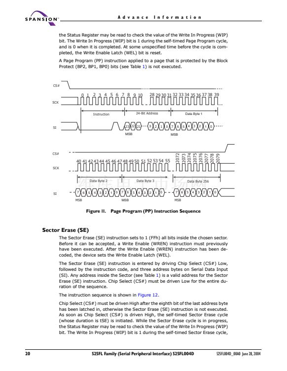
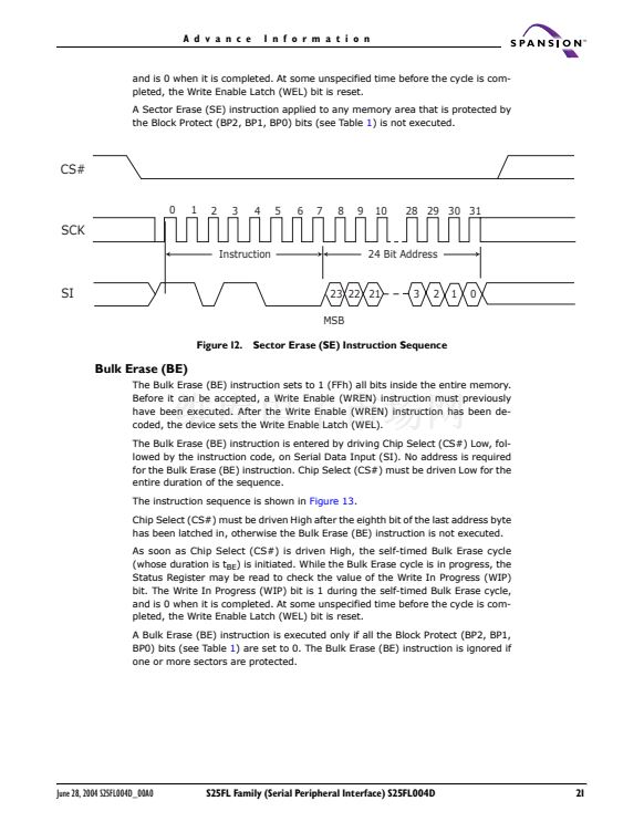
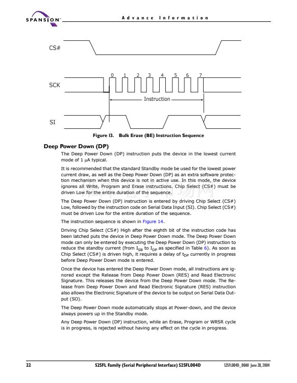
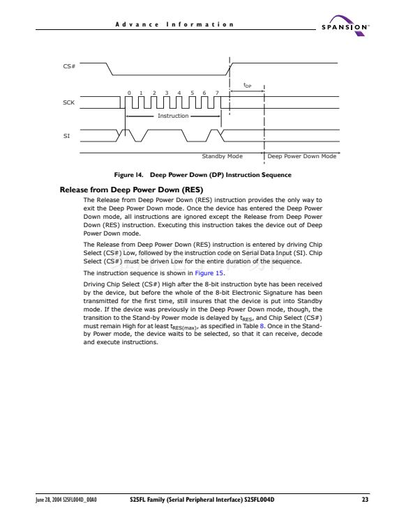
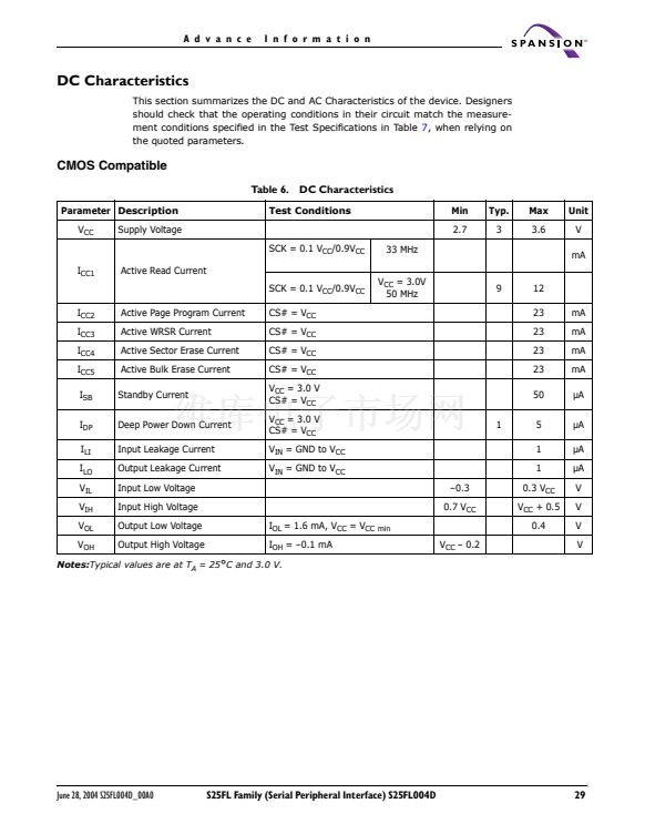
A d v a n c e
I n f o r m a t i o n
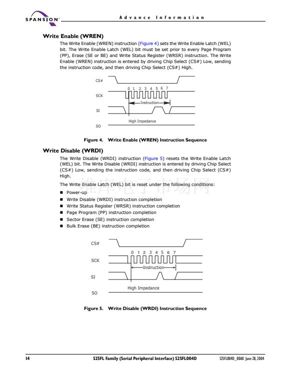
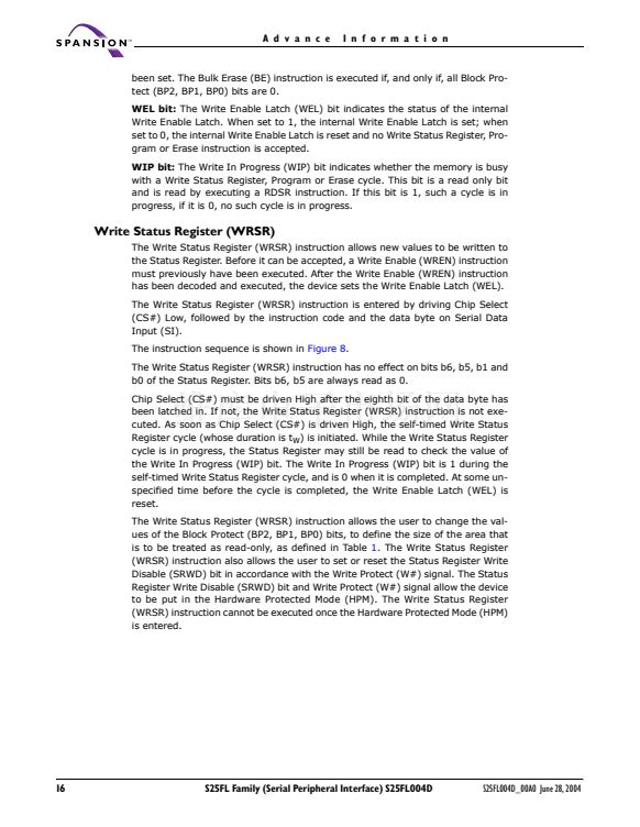
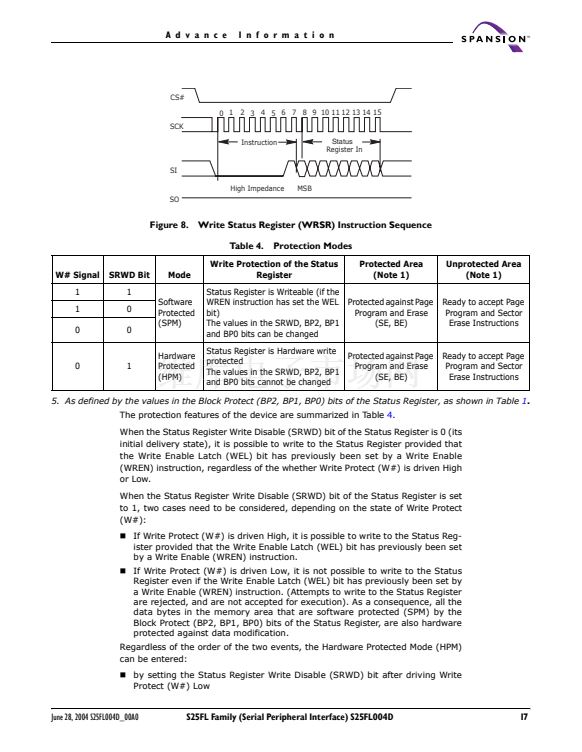
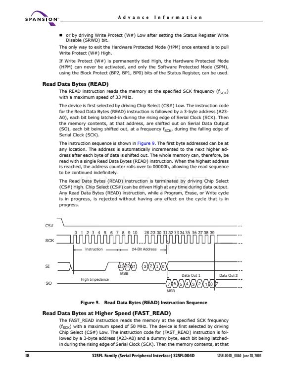
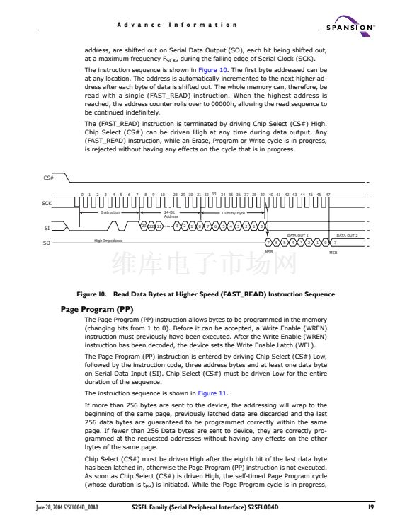
Write Enable (WREN)
The Write Enable (WREN) instruction (Figure
4)
sets the Write Enable Latch (WEL)
bit. The Write Enable Latch (WEL) bit must be set prior to every Page Program
(PP), Erase (SE or BE) and Write Status Register (WRSR) instruction. The Write
Enable (WREN) instruction is entered by driving Chip Select (CS#) Low, sending
the instruction code, and then driving Chip Select (CS#) High.
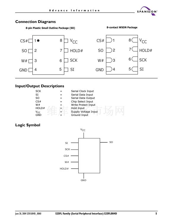
CS#
0 1
SCK
Instruction
SI
High Impedance
SO
2 3 4 5 6 7
Figure 4. Write Enable (WREN) Instruction Sequence
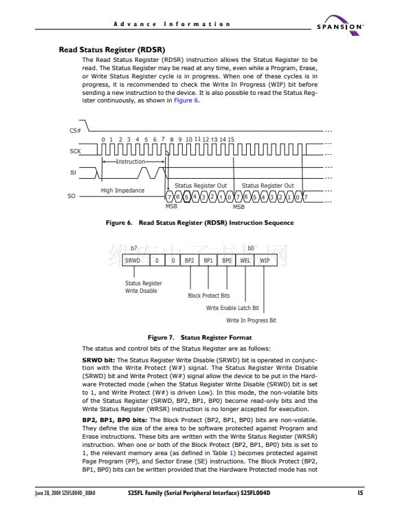
Write Disable (WRDI)
The Write Disable (WRDI) instruction (Figure
5)
resets the Write Enable Latch
(WEL) bit. The Write Disable (WRDI) instruction is entered by driving Chip Select
(CS#) Low, sending the instruction code, and then driving Chip Select (CS#)
High.
The Write Enable Latch (WEL) bit is reset under the following conditions:
Power-up
Write Disable (WRDI) instruction completion
Write Status Register (WRSR) instruction completion
Page Program (PP) instruction completion
Sector Erase (SE) instruction completion
Bulk Erase (BE) instruction completion
CS#
0
1 2
3 4 5
6 7
SCK
Instruction
SI
High Impedance
SO
Figure 5.
Write Disable (WRDI) Instruction Sequence
14
S25FL Family (Serial Peripheral Interface) S25FL004D
S25FL004D_00A0 June 28, 2004


 1
1
 2
2
 3
3
 4
4
 5
5
 6
6
 7
7
 8
8
 9
9
 10
10
 11
11
 12
12
 13
13
 14
14
 15
15
 16
16
 17
17
 18
18
 19
19
 20
20
 21
21
 22
22
 23
23
 24
24
 25
25
 26
26
 27
27
 28
28
 29
29
 30
30
 31
31
 32
32
 33
33
 34
34
 35
35
 36
36
