Philips Semiconductors
SC16C654B/654DB
5 V, 3.3 V and 2.5 V quad UART, 5 Mbit/s (max.) with 64-byte FIFOs
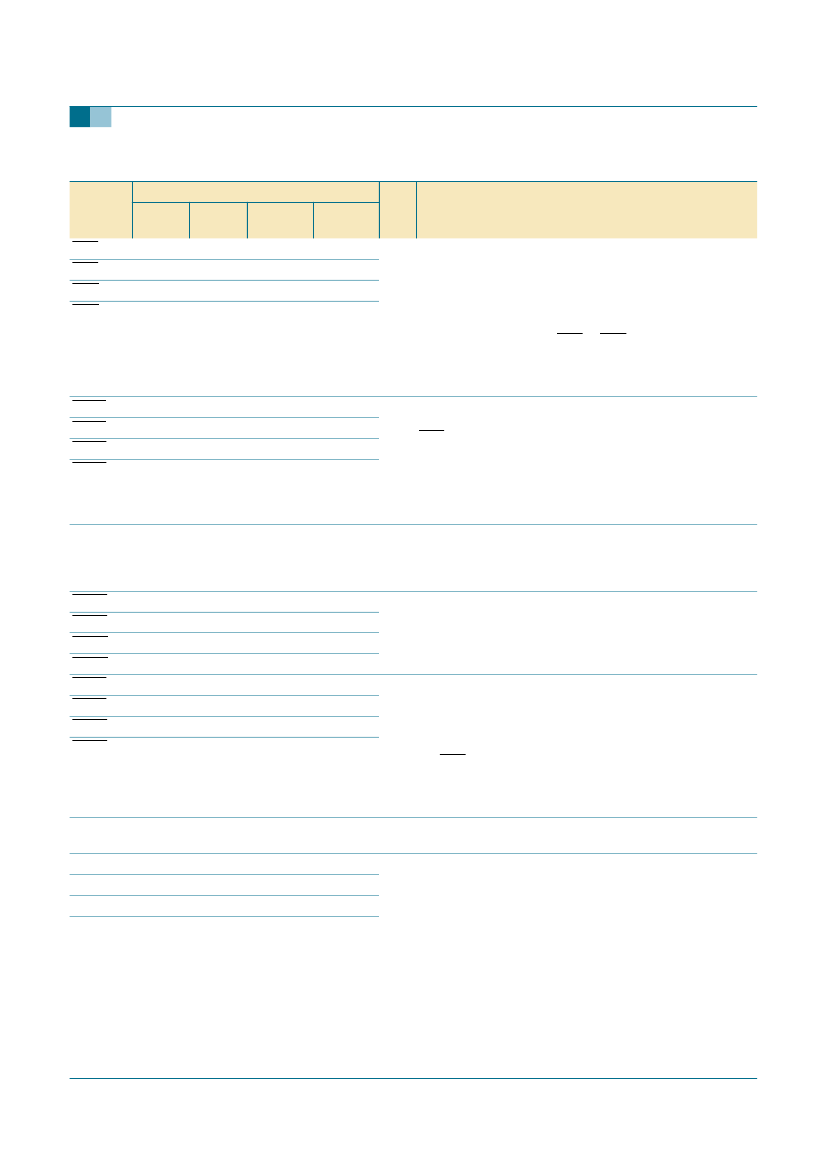
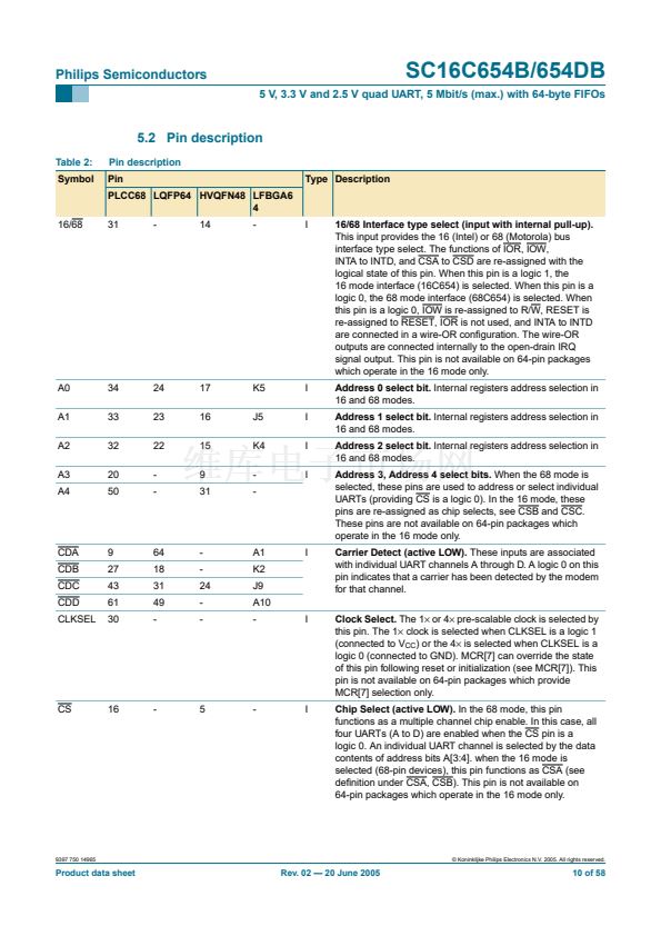
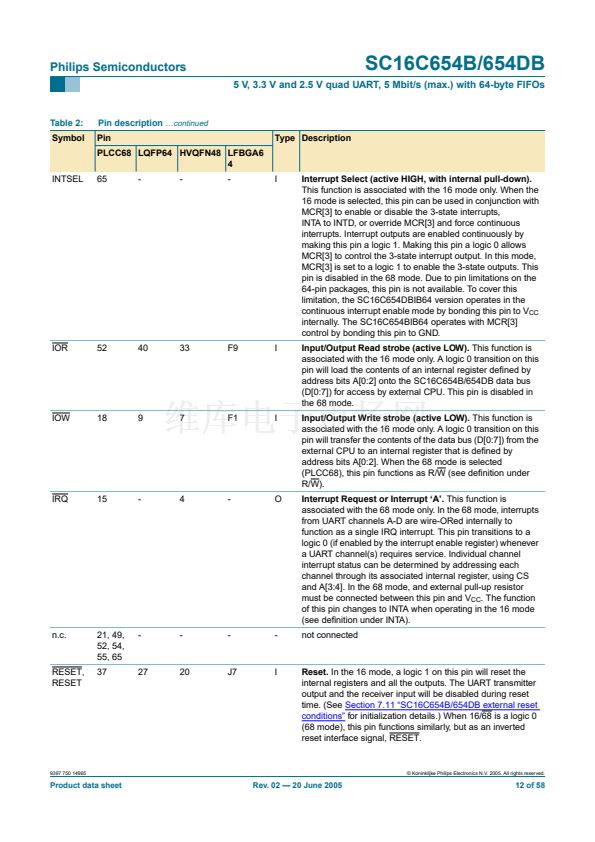
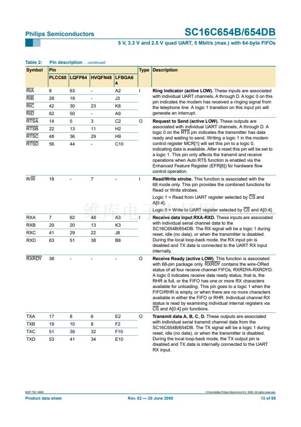
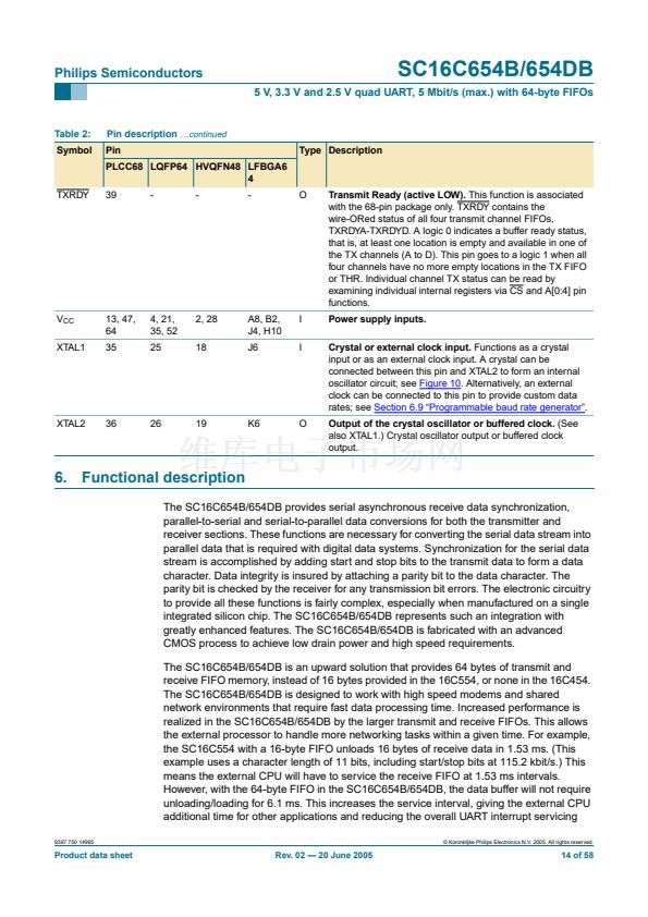
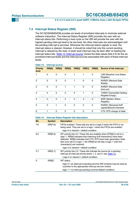
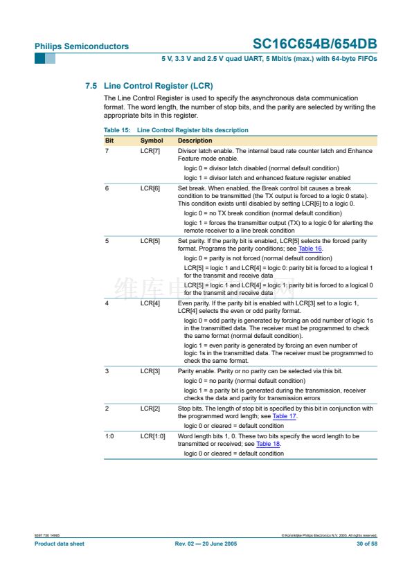
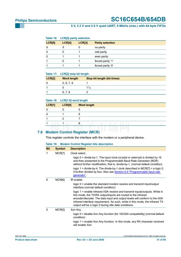
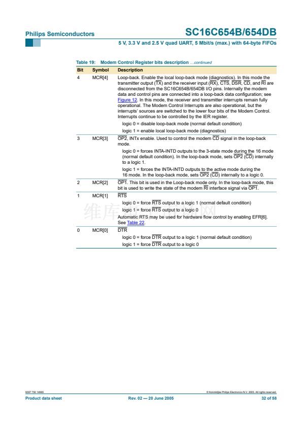
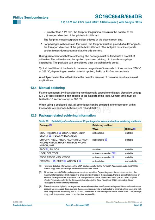
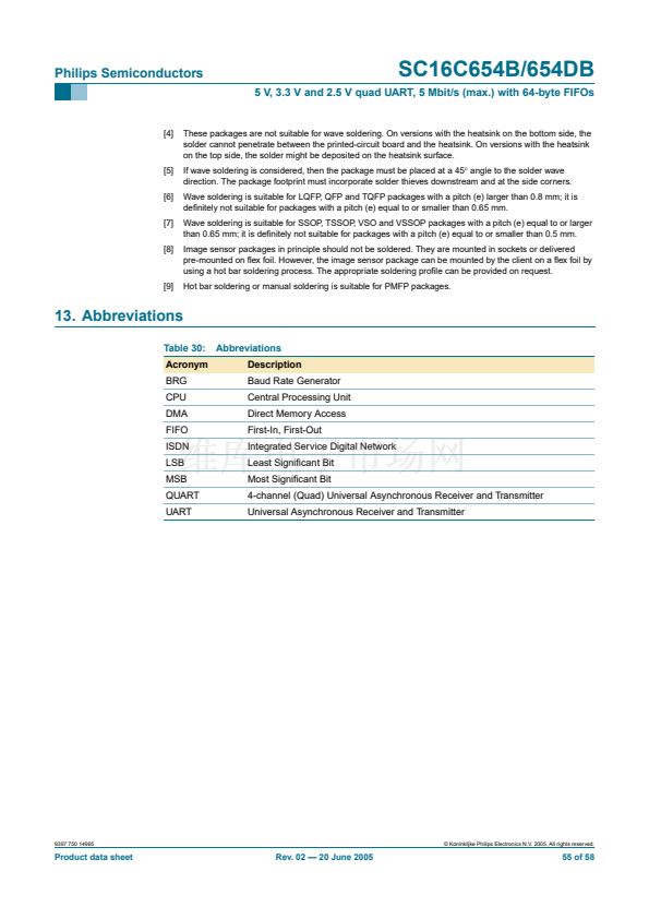
Table 2:
Symbol
Pin description
鈥ontinued
Pin
PLCC68 LQFP64 HVQFN48 LFBGA6
4
Type Description
CSA
CSB
CSC
CSD
16
20
50
54
7
11
38
42
5
9
31
35
E1
G1
G9
E9
I
Chip Select A, B, C, D (active LOW).
This function is
associated with the 16 mode only, and for individual
channels 鈥楢鈥?through 鈥楧鈥? When in 16 mode, these pins
enable data transfers between the user CPU and the
SC16C654B/654DB for the channel(s) addressed. Individual
UART sections (A, B, C, D) are addressed by providing a
logic 0 on the respective CSA to CSD pin. When the
68 mode is selected, the functions of these pins are
re-assigned. 68 mode functions are described under their
respective name/pin headings.
Clear to Send (active LOW).
These inputs are associated
with individual UART channels A through D. A logic 0 on the
CTS pin indicates the modem or data set is ready to accept
transmit data from the SC16C654B/654DB. Status can be
tested by reading MSR[4]. This pin only affects the transmit
or receive operations when Auto CTS function is enabled via
the Enhanced Feature Register EFR[7] for hardware 铿俹w
control operation.
Data bus (bi-directional).
These pins are the 8-bit, 3-state
data bus for transferring information to or from the controlling
CPU. D0 is the least signi铿乧ant bit and the 铿乺st data bit in a
transmit or receive serial data stream.
Data Set Ready (active LOW).
These inputs are associated
with individual UART channels, A through D. A logic 0 on this
pin indicates the modem or data set is powered-on and is
ready for data exchange with the UART. This pin has no
effect on the UART鈥檚 transmit or receive operation.
Data Terminal Ready (active LOW).
These outputs are
associated with individual UART channels, A through D. A
logic 0 on this pin indicates that the SC16C654B/654DB is
powered-on and ready. This pin can be controlled via the
modem control register. Writing a logic 1 to MCR[0] will set
the DTR output to logic 0, enabling the modem. This pin will
be a logic 1 after writing a logic 0 to MCR[0], or after a reset.
This pin has no effect on the UART鈥檚 transmit or receive
operation.
Signal and power ground.
Interrupt A, B, C, D (active HIGH).
This function is
associated with the 16 mode only. These pins provide
individual channel interrupts INTA to INTD. INTA to INTD are
enabled when MCR[3] is set to a logic 1, interrupts are
enabled in the interrupt enable register (IER), and when an
interrupt condition exists. Interrupt conditions include:
receiver errors, available receiver buffer data, transmit buffer
empty, or when a modem status 铿俛g is detected. When the
68 mode is selected, the functions of these pins are
re-assigned. 68 mode functions are described under their
respective name/pin headings.
CTSA
CTSB
CTSC
CTSD
11
25
45
59
2
16
33
47
1
12
26
-
C1
J2
K10
B10
I
D0 to D2, 66 to 68 53 to 55, 39 to 41,
D3 to D7 , 1 to 5 56 to 60 42 to 46
B7, A7,
B6, A6,
B5, A5,
B4, A4
B1
K1
K9
B9
D1
J1
J10
C9
I/O
DSRA
DSRB
DSRC
DSRD
DTRA
DTRB
DTRC
DTRD
10
26
44
60
12
24
46
58
1
17
32
48
3
15
34
46
-
-
25
-
-
-
27
-
I
O
GND
INTA
INTB
INTC
INTD
6, 23,
40, 57
15
21
49
55
14, 28,
45, 61
6
12
37
43
21, 37, 47 B3, K7,
H1, D9
4
10
30
36
D2
G2
G10
D10
I
O
9397 750 14965
漏 Koninklijke Philips Electronics N.V. 2005. All rights reserved.
Product data sheet
Rev. 02 鈥?20 June 2005
11 of 58


 1
1
 2
2
 3
3
 4
4
 5
5
 6
6
 7
7
 8
8
 9
9
 10
10
 11
11
 12
12
 13
13
 14
14
 15
15
 16
16
 17
17
 18
18
 19
19
 20
20
 21
21
 22
22
 23
23
 24
24
 25
25
 26
26
 27
27
 28
28
 29
29
 30
30
 31
31
 32
32
 33
33
 34
34
 35
35
 36
36
 37
37
 38
38
 39
39
 40
40
 41
41
 42
42
 43
43
 44
44
 45
45
 46
46
 47
47
 48
48
 49
49
 50
50
 51
51
 52
52
 53
53
 54
54
 55
55
 56
56
 57
57
 58
58
