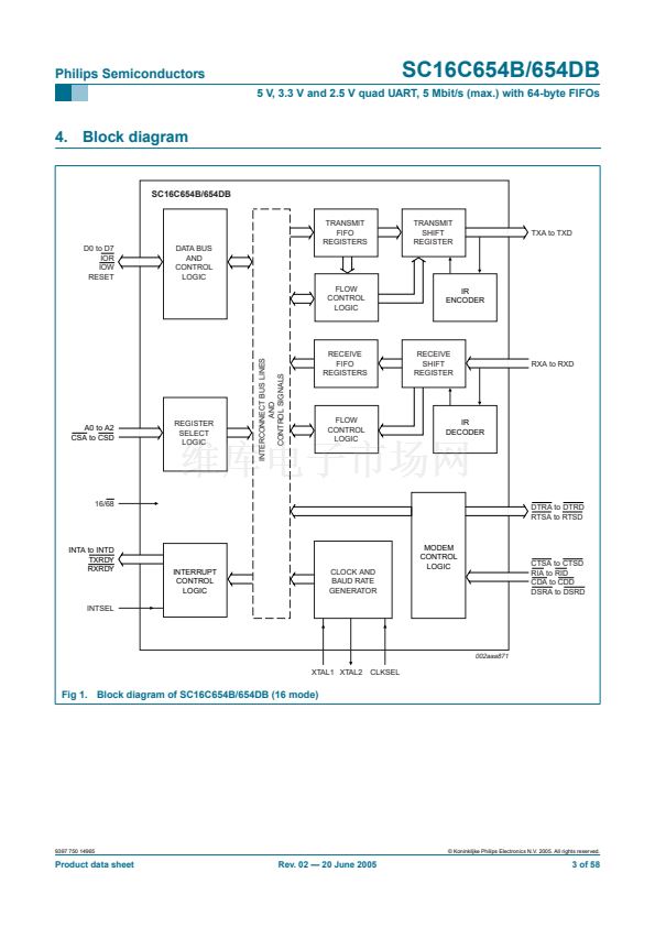
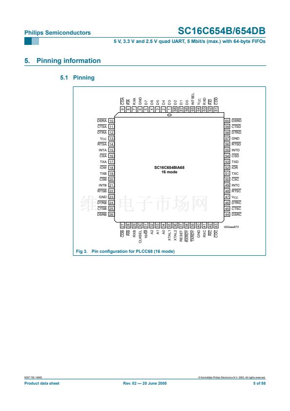
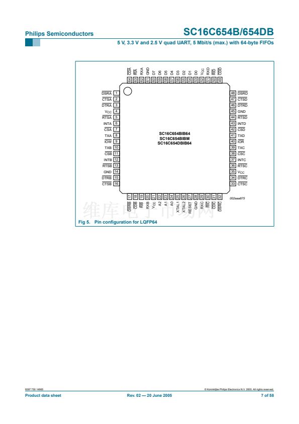
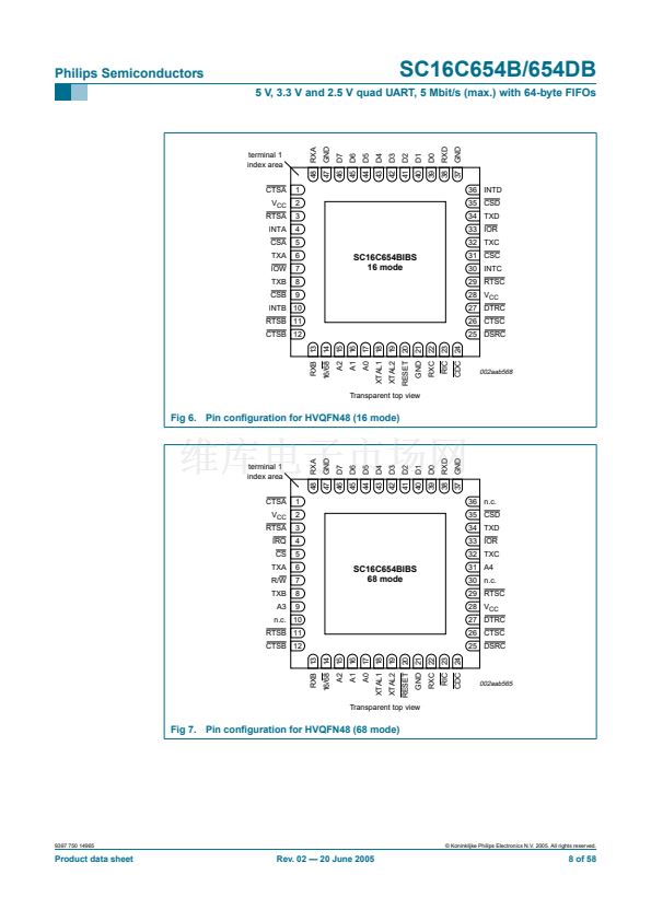
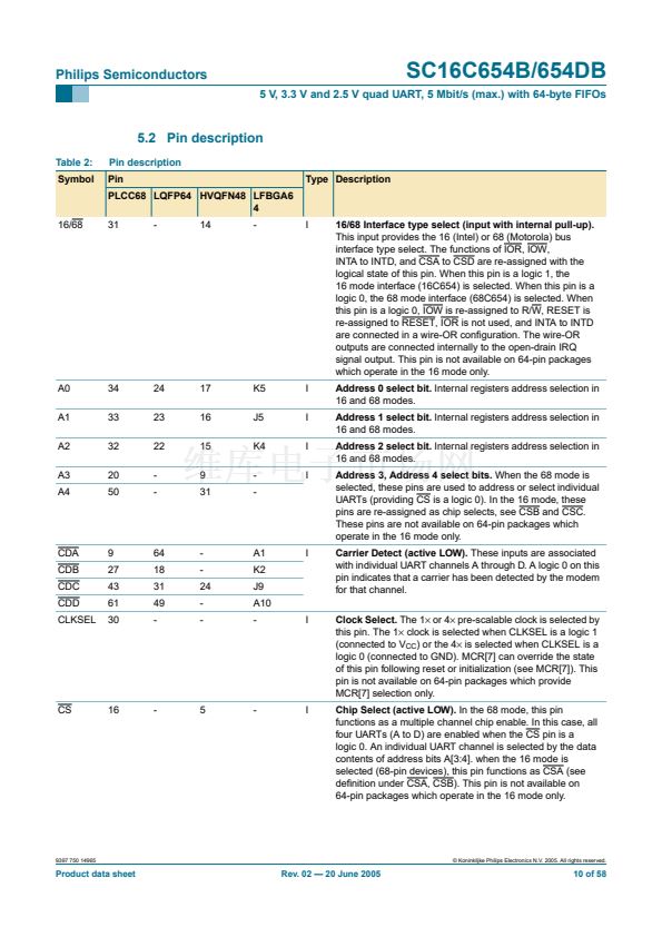
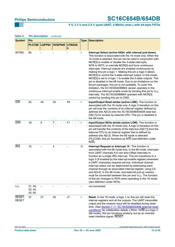
Philips Semiconductors
SC16C654B/654DB
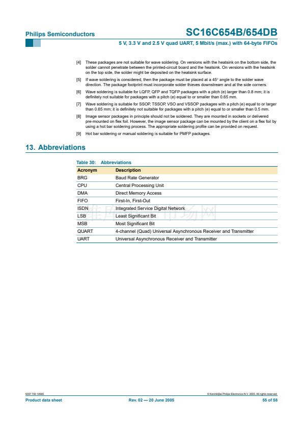
5 V, 3.3 V and 2.5 V quad UART, 5 Mbit/s (max.) with 64-byte FIFOs
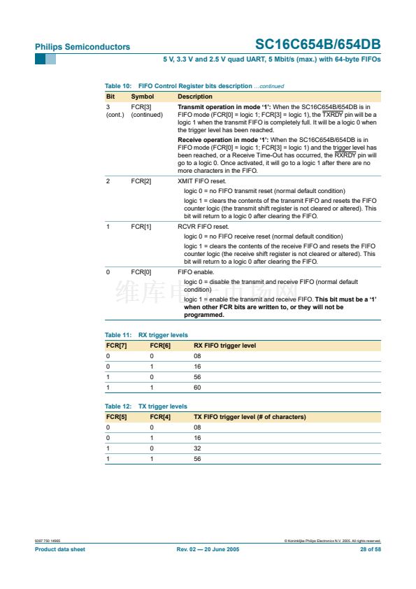
FIFO Control Register bits description
鈥ontinued
Description
Transmit operation in mode 鈥?鈥?
When the SC16C654B/654DB is in
FIFO mode (FCR[0] = logic 1; FCR[3] = logic 1), the TXRDY pin will be a
logic 1 when the transmit FIFO is completely full. It will be a logic 0 when
the trigger level has been reached.
Receive operation in mode 鈥?鈥?
When the SC16C654B/654DB is in
FIFO mode (FCR[0] = logic 1; FCR[3] = logic 1) and the trigger level has
been reached, or a Receive Time-Out has occurred, the RXRDY pin will
go to a logic 0. Once activated, it will go to a logic 1 after there are no
more characters in the FIFO.
Table 10:
Bit
3
(cont.)
Symbol
FCR[3]
(continued)
2
FCR[2]
XMIT FIFO reset.
logic 0 = no FIFO transmit reset (normal default condition)
logic 1 = clears the contents of the transmit FIFO and resets the FIFO
counter logic (the transmit shift register is not cleared or altered). This
bit will return to a logic 0 after clearing the FIFO.
1
FCR[1]
RCVR FIFO reset.
logic 0 = no FIFO receive reset (normal default condition)
logic 1 = clears the contents of the receive FIFO and resets the FIFO
counter logic (the receive shift register is not cleared or altered). This
bit will return to a logic 0 after clearing the FIFO.
0
FCR[0]
FIFO enable.
logic 0 = disable the transmit and receive FIFO (normal default
condition)
logic 1 = enable the transmit and receive FIFO.
This bit must be a 鈥?鈥?/div>
when other FCR bits are written to, or they will not be
programmed.
Table 11:
FCR[7]
0
0
1
1
Table 12:
FCR[5]
0
0
1
1
RX trigger levels
FCR[6]
0
1
0
1
TX trigger levels
FCR[4]
0
1
0
1
TX FIFO trigger level (# of characters)
08
16
32
56
RX FIFO trigger level
08
16
56
60
9397 750 14965
漏 Koninklijke Philips Electronics N.V. 2005. All rights reserved.
Product data sheet
Rev. 02 鈥?20 June 2005
28 of 58


 1
1
 2
2
 3
3
 4
4
 5
5
 6
6
 7
7
 8
8
 9
9
 10
10
 11
11
 12
12
 13
13
 14
14
 15
15
 16
16
 17
17
 18
18
 19
19
 20
20
 21
21
 22
22
 23
23
 24
24
 25
25
 26
26
 27
27
 28
28
 29
29
 30
30
 31
31
 32
32
 33
33
 34
34
 35
35
 36
36
 37
37
 38
38
 39
39
 40
40
 41
41
 42
42
 43
43
 44
44
 45
45
 46
46
 47
47
 48
48
 49
49
 50
50
 51
51
 52
52
 53
53
 54
54
 55
55
 56
56
 57
57
 58
58
