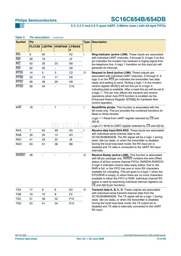
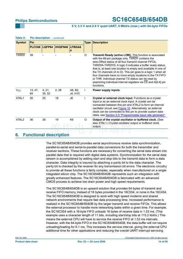
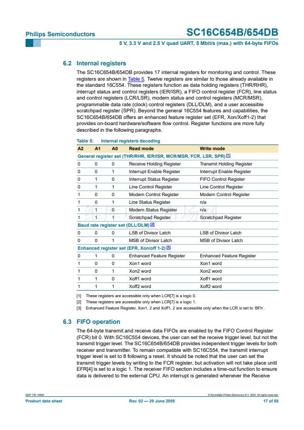
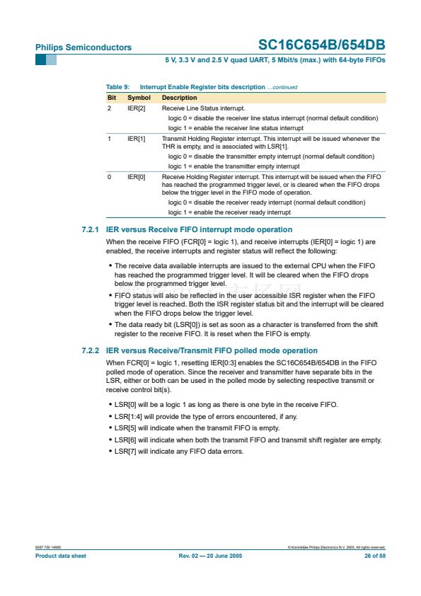
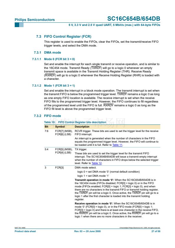
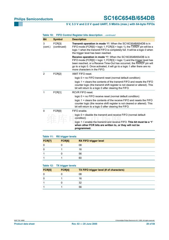
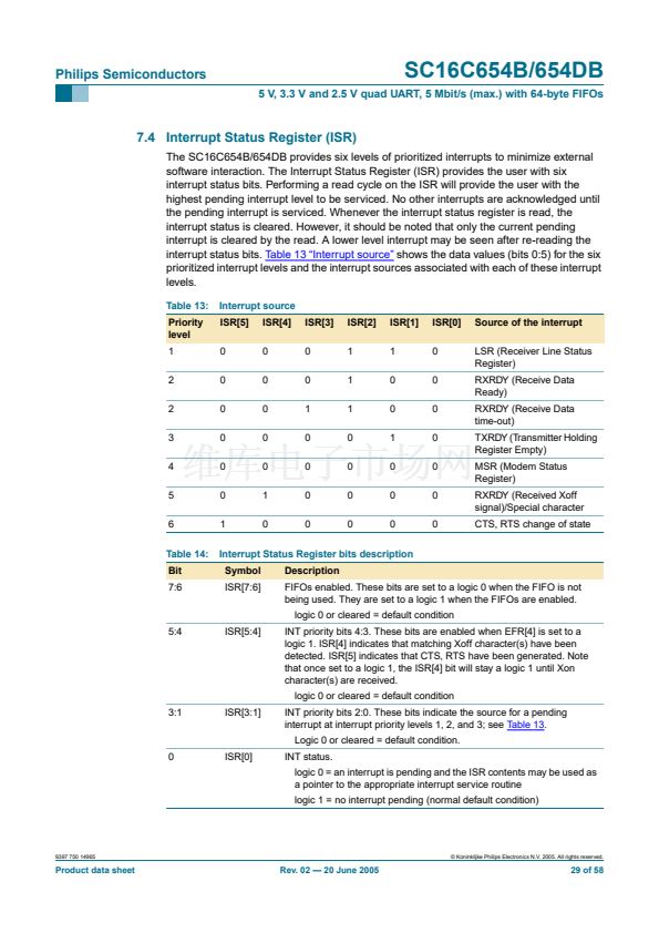
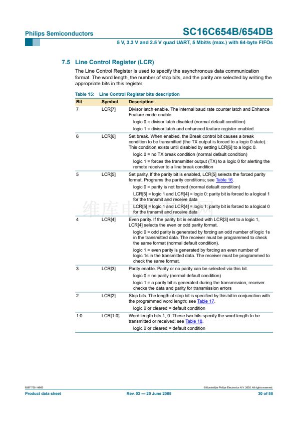
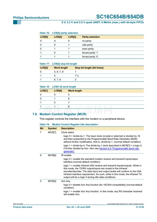
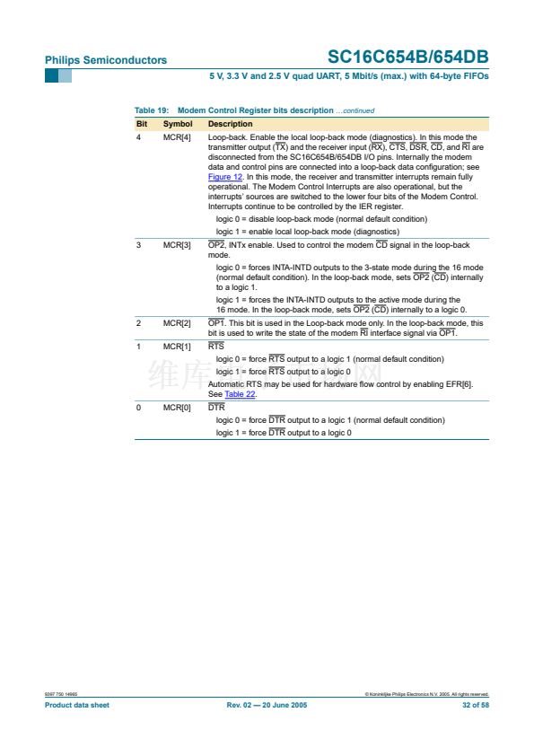
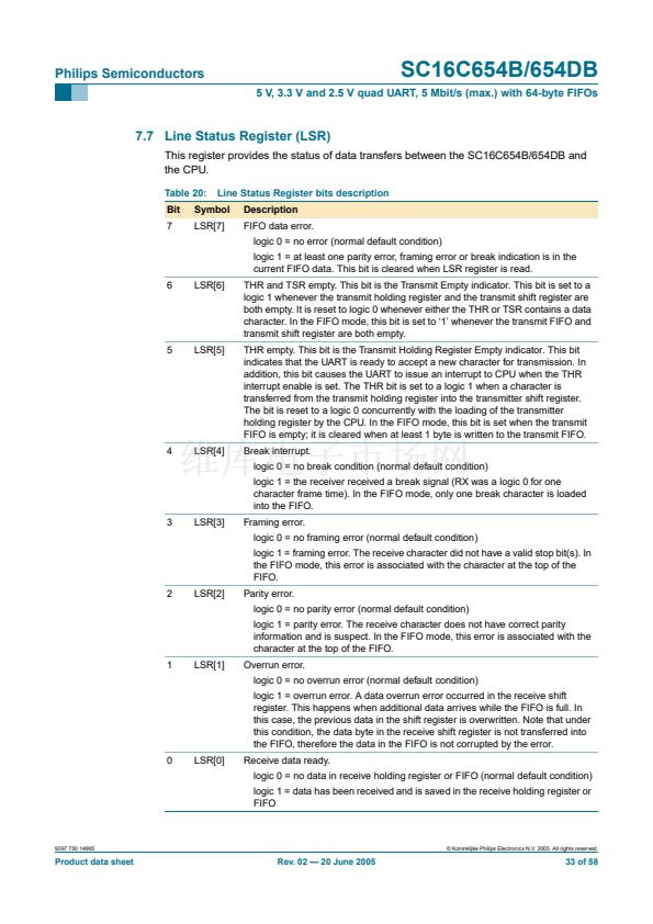
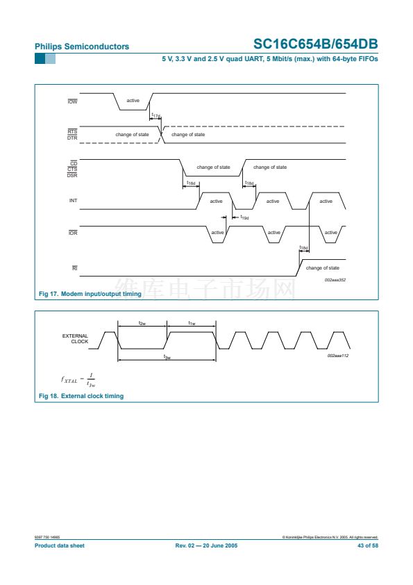
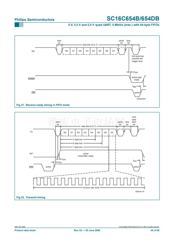
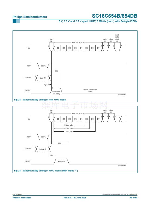
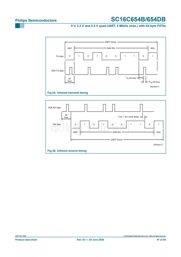
Philips Semiconductors
SC16C654B/654DB
5 V, 3.3 V and 2.5 V quad UART, 5 Mbit/s (max.) with 64-byte FIFOs
When two interrupt conditions have the same priority, it is important to service these
interrupts correctly. Receive Data Ready and Receive Time Out have the same interrupt
priority (when enabled by IER[0]). The receiver issues an interrupt after the number of
characters have reached the programmed trigger level. In this case, the
SC16C654B/654DB FIFO may hold more characters than the programmed trigger level.
Following the removal of a data byte, the user should re-check LSR[0] for additional
characters. A Receive Time Out will not occur if the receive FIFO is empty. The time-out
counter is reset at the center of each stop bit received or each time the receive holding
register (RHR) is read. The actual time-out value is 4 character time.
In the 16 mode for the PLCC68 package, the system/board designer can optionally
provide software controlled 3-state interrupt operation. This is accomplished by INTSEL
and MCR[3]. When INTSEL interface pin is left open or made a logic 0, MCR[3] controls
the 3-state interrupt outputs, INTA to INTD. When INTSEL is a logic 1, MCR[3] has no
effect on the INTA to INTD outputs, and the package operates with interrupt outputs
enabled continuously.
6.9 Programmable baud rate generator
The SC16C654B/654DB supports high speed modem technologies that have increased
input data rates by employing data compression schemes. For example, a 33.6 kbit/s
modem that employs data compression may require a 115.2 kbit/s input data rate.
A 128.0 kbit/s ISDN modem that supports data compression may need an input data rate
of 460.8 kbit/s.
A single baud rate generator is provided for the transmitter and receiver, allowing
independent TX/RX channel control. The programmable Baud Rate Generator is capable
of accepting an input clock up to 80 MHz (for 3.3 V and 5 V operation), as required for
supporting a 5 Mbit/s data rate. The SC16C654B/654DB can be con铿乬ured for internal or
external clock operation. For internal clock oscillator operation, an industry standard
microprocessor crystal (parallel resonant/22 pF to 33 pF load) is connected externally
between the XTAL1 and XTAL2 pins; see
Figure 10.
Alternatively, an external clock can be
connected to the XTAL1 pin to clock the internal baud rate generator for standard or
custom rates; see
Table 7.
XTAL1
XTAL2
XTAL1
XTAL2
1.5 k鈩?/div>
X1
1.8432 MHz
X1
1.8432 MHz
C1
22 pF
C2
33 pF
C1
22 pF
C2
47 pF
002aaa870
Fig 10. Crystal oscillator connection
The generator divides the input 16脳 clock by any divisor from 1 to (2
16
鈭?/div>
1). The
SC16C654B/654DB divides the basic external clock by 16. Further division of this 16脳
clock provides two table rates to support low and high data rate applications using the
same system design. After a hardware reset and during initialization, the
9397 750 14965
漏 Koninklijke Philips Electronics N.V. 2005. All rights reserved.
Product data sheet
Rev. 02 鈥?20 June 2005
20 of 58


 1
1
 2
2
 3
3
 4
4
 5
5
 6
6
 7
7
 8
8
 9
9
 10
10
 11
11
 12
12
 13
13
 14
14
 15
15
 16
16
 17
17
 18
18
 19
19
 20
20
 21
21
 22
22
 23
23
 24
24
 25
25
 26
26
 27
27
 28
28
 29
29
 30
30
 31
31
 32
32
 33
33
 34
34
 35
35
 36
36
 37
37
 38
38
 39
39
 40
40
 41
41
 42
42
 43
43
 44
44
 45
45
 46
46
 47
47
 48
48
 49
49
 50
50
 51
51
 52
52
 53
53
 54
54
 55
55
 56
56
 57
57
 58
58
