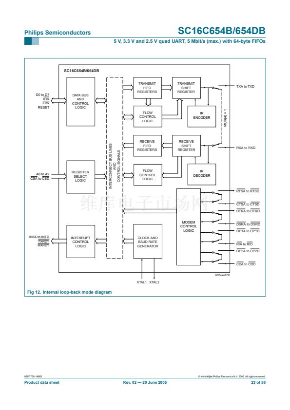
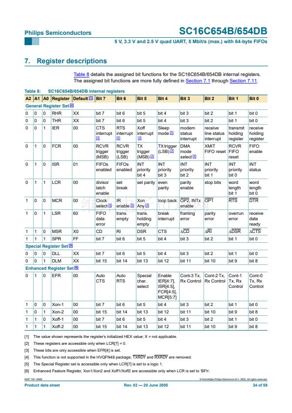
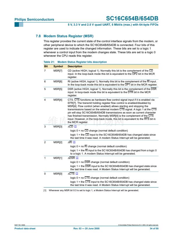
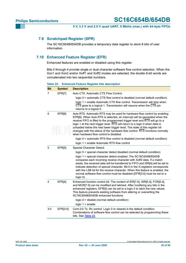
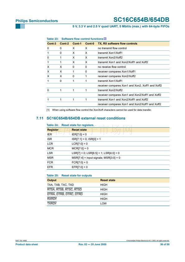
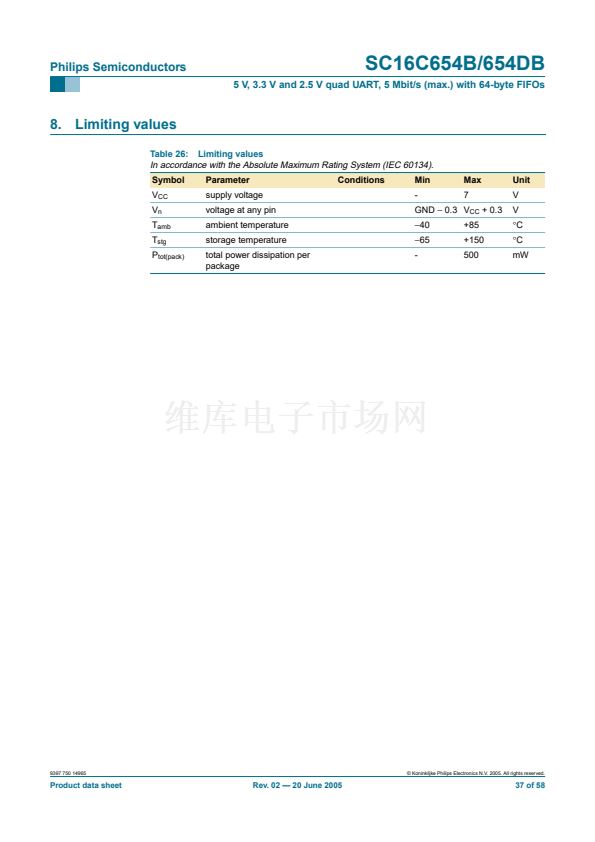
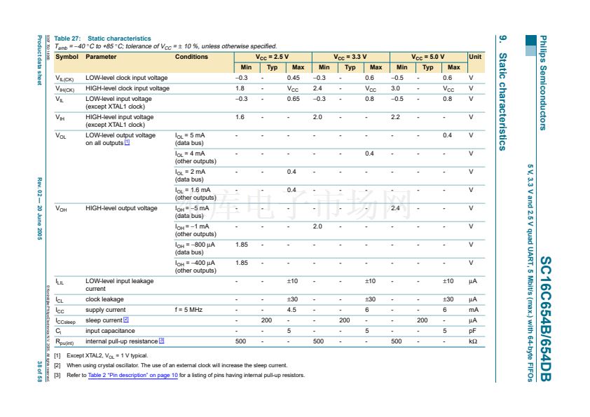
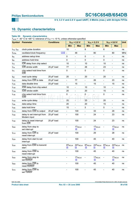
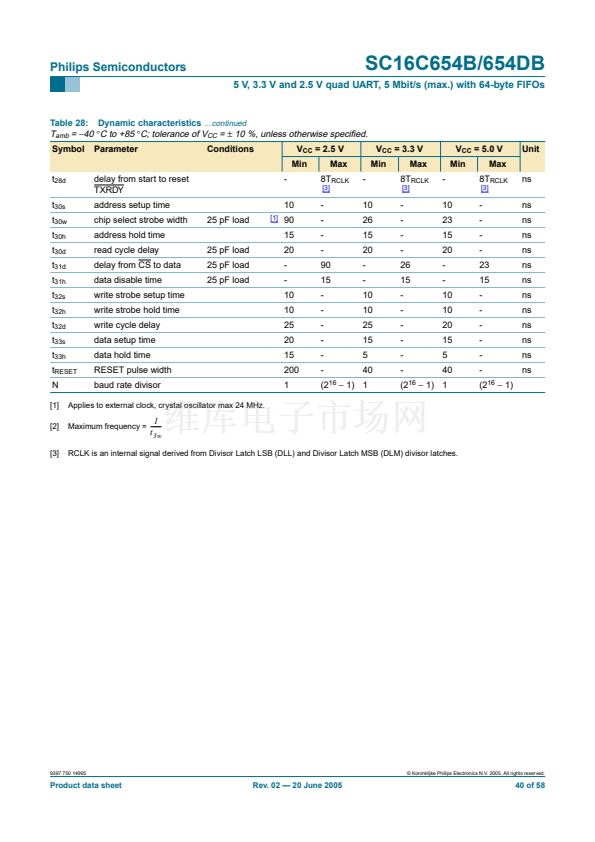
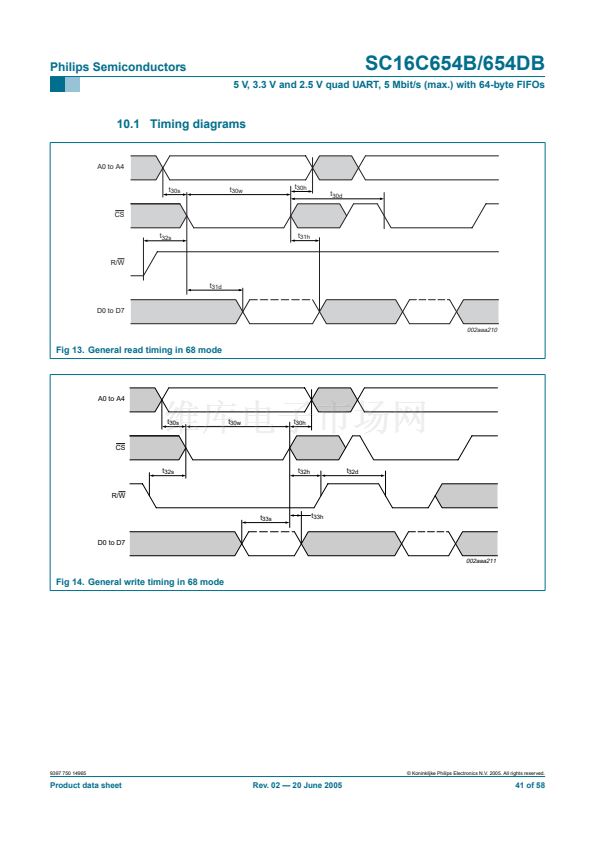
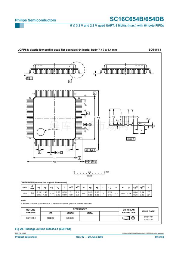
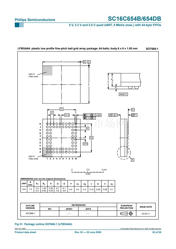
Philips Semiconductors
SC16C654B/654DB
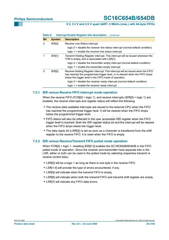
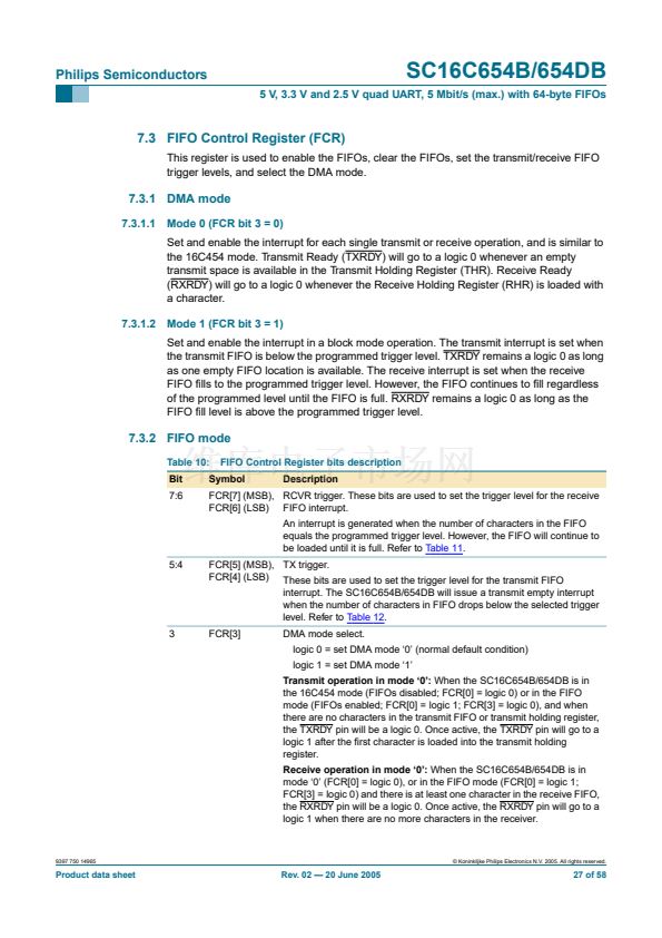
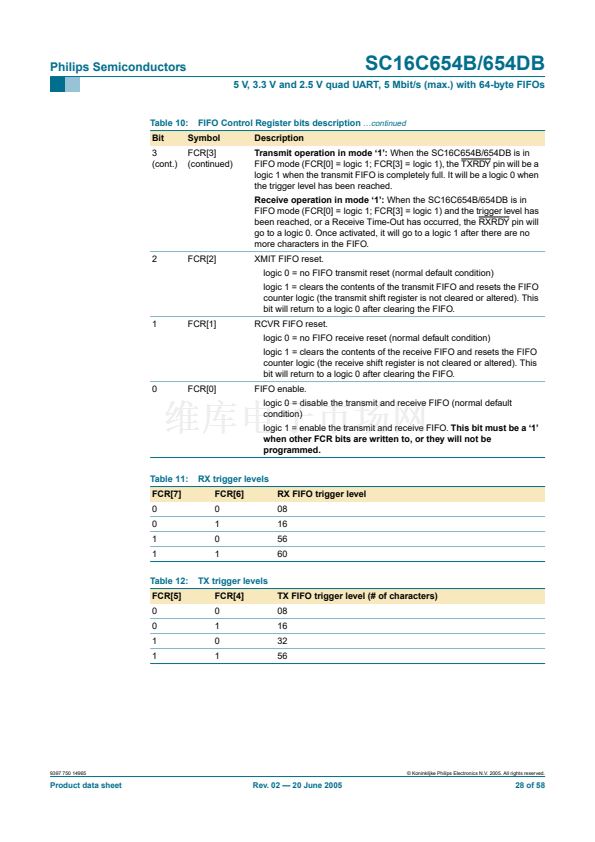
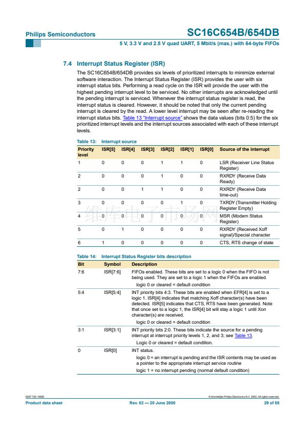
5 V, 3.3 V and 2.5 V quad UART, 5 Mbit/s (max.) with 64-byte FIFOs
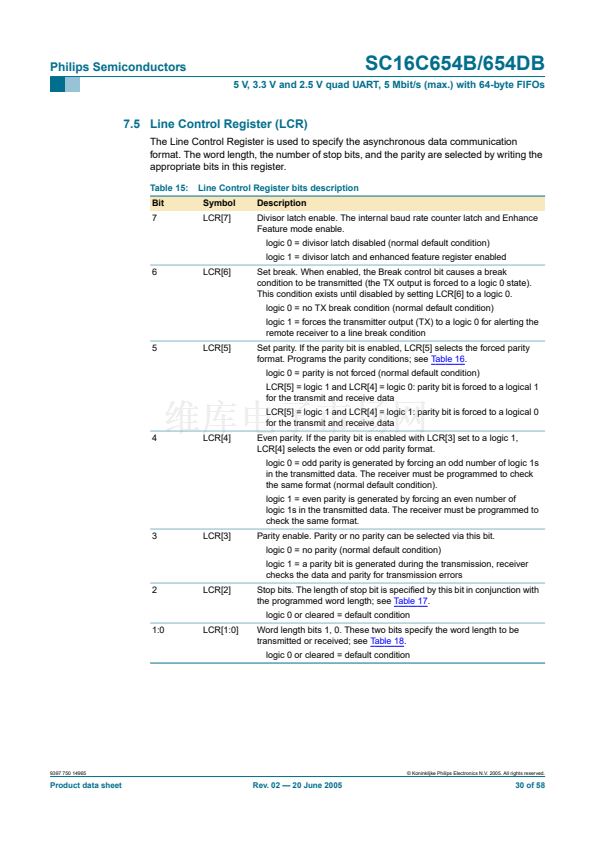
7.5 Line Control Register (LCR)
The Line Control Register is used to specify the asynchronous data communication
format. The word length, the number of stop bits, and the parity are selected by writing the
appropriate bits in this register.
Table 15:
Bit
7
Line Control Register bits description
Symbol
LCR[7]
Description
Divisor latch enable. The internal baud rate counter latch and Enhance
Feature mode enable.
logic 0 = divisor latch disabled (normal default condition)
logic 1 = divisor latch and enhanced feature register enabled
6
LCR[6]
Set break. When enabled, the Break control bit causes a break
condition to be transmitted (the TX output is forced to a logic 0 state).
This condition exists until disabled by setting LCR[6] to a logic 0.
logic 0 = no TX break condition (normal default condition)
logic 1 = forces the transmitter output (TX) to a logic 0 for alerting the
remote receiver to a line break condition
5
LCR[5]
Set parity. If the parity bit is enabled, LCR[5] selects the forced parity
format. Programs the parity conditions; see
Table 16.
logic 0 = parity is not forced (normal default condition)
LCR[5] = logic 1 and LCR[4] = logic 0: parity bit is forced to a logical 1
for the transmit and receive data
LCR[5] = logic 1 and LCR[4] = logic 1: parity bit is forced to a logical 0
for the transmit and receive data
4
LCR[4]
Even parity. If the parity bit is enabled with LCR[3] set to a logic 1,
LCR[4] selects the even or odd parity format.
logic 0 = odd parity is generated by forcing an odd number of logic 1s
in the transmitted data. The receiver must be programmed to check
the same format (normal default condition).
logic 1 = even parity is generated by forcing an even number of
logic 1s in the transmitted data. The receiver must be programmed to
check the same format.
3
LCR[3]
Parity enable. Parity or no parity can be selected via this bit.
logic 0 = no parity (normal default condition)
logic 1 = a parity bit is generated during the transmission, receiver
checks the data and parity for transmission errors
2
LCR[2]
Stop bits. The length of stop bit is speci铿乪d by this bit in conjunction with
the programmed word length; see
Table 17.
logic 0 or cleared = default condition
1:0
LCR[1:0]
Word length bits 1, 0. These two bits specify the word length to be
transmitted or received; see
Table 18.
logic 0 or cleared = default condition
9397 750 14965
漏 Koninklijke Philips Electronics N.V. 2005. All rights reserved.
Product data sheet
Rev. 02 鈥?20 June 2005
30 of 58


 1
1
 2
2
 3
3
 4
4
 5
5
 6
6
 7
7
 8
8
 9
9
 10
10
 11
11
 12
12
 13
13
 14
14
 15
15
 16
16
 17
17
 18
18
 19
19
 20
20
 21
21
 22
22
 23
23
 24
24
 25
25
 26
26
 27
27
 28
28
 29
29
 30
30
 31
31
 32
32
 33
33
 34
34
 35
35
 36
36
 37
37
 38
38
 39
39
 40
40
 41
41
 42
42
 43
43
 44
44
 45
45
 46
46
 47
47
 48
48
 49
49
 50
50
 51
51
 52
52
 53
53
 54
54
 55
55
 56
56
 57
57
 58
58
