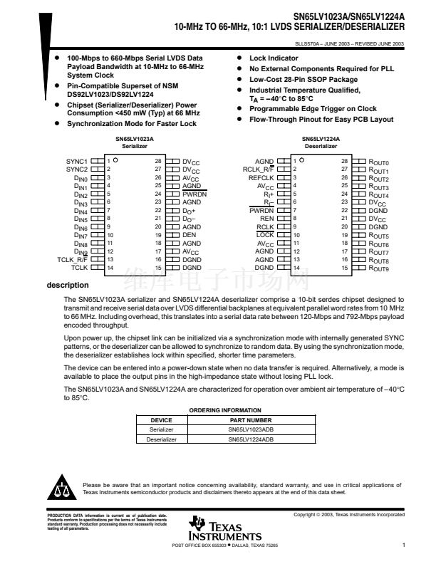
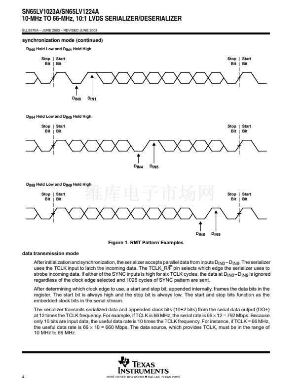
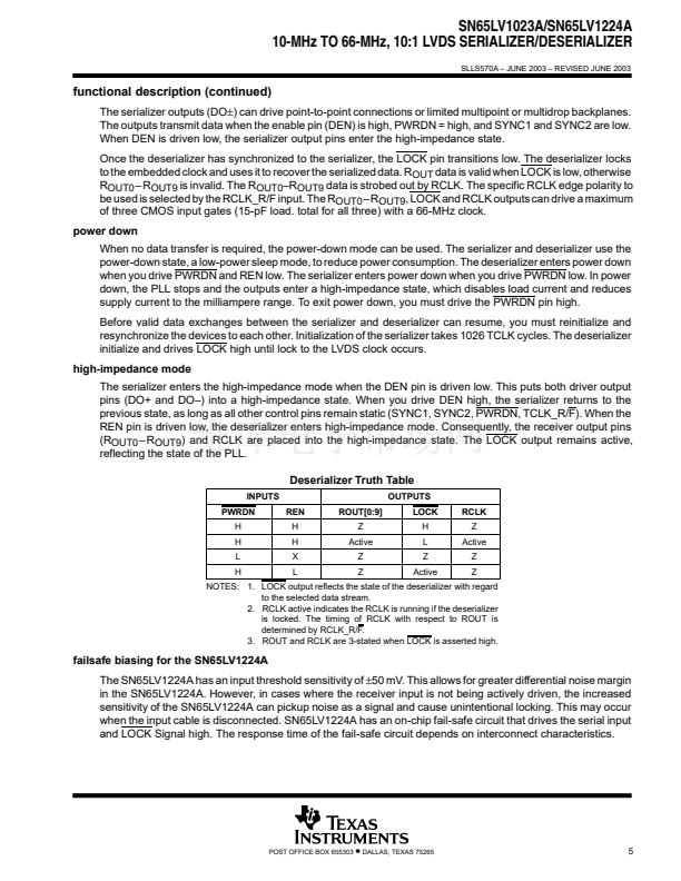
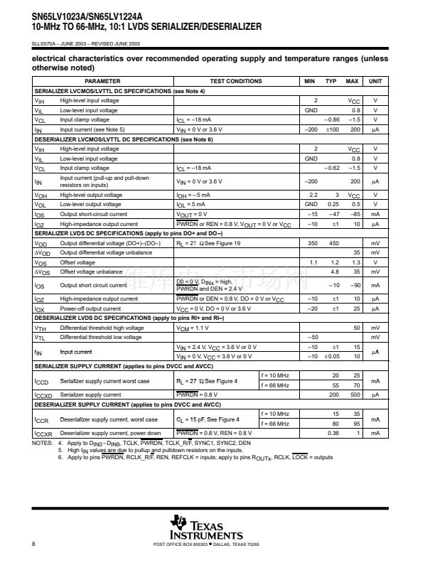
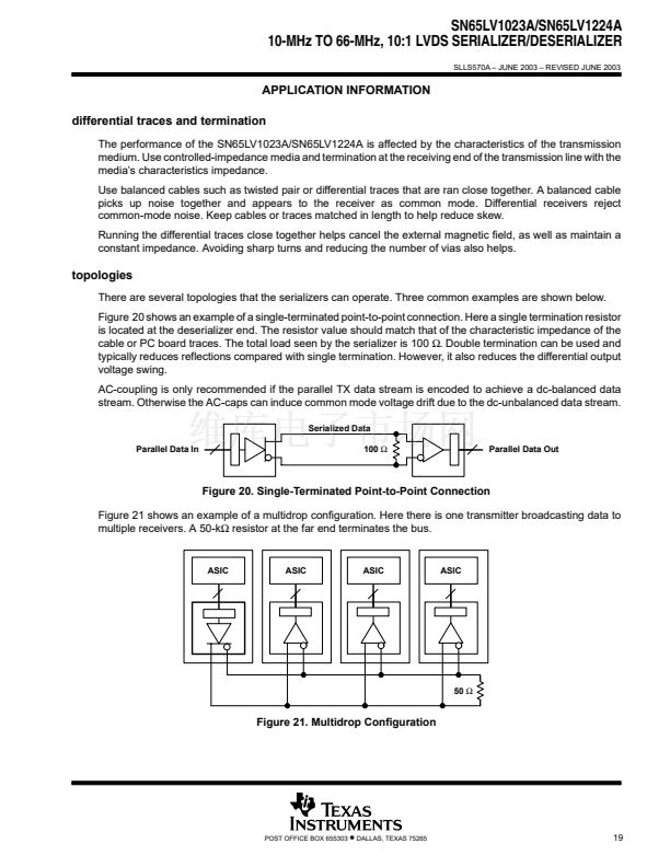
鈥?/div>
V
CC
to GND . . . . . . . . . . . . . . . . . . . . . . . . . . . . . . . . . . . . . . . . . . . . . . . . . . . . . . . . . . . . . . . . . . . . . . 鈥?0.3 V to 4 V
LVTTL input voltage . . . . . . . . . . . . . . . . . . . . . . . . . . . . . . . . . . . . . . . . . . . . . . . . . . . . . . . 鈥?0.3 V to (V
CC
+ 0.3 V)
LVTTL output voltage . . . . . . . . . . . . . . . . . . . . . . . . . . . . . . . . . . . . . . . . . . . . . . . . . . . . . . 鈥?0.3 V to (V
CC
+ 0.3 V)
LVDS receiver input voltage . . . . . . . . . . . . . . . . . . . . . . . . . . . . . . . . . . . . . . . . . . . . . . . . . . . . . . . . 鈥?0.3 V to 3.9 V
LVDS driver output voltage . . . . . . . . . . . . . . . . . . . . . . . . . . . . . . . . . . . . . . . . . . . . . . . . . . . . . . . . . 鈥?0.3 V to 3.9 V
LVDS output short circuit duration . . . . . . . . . . . . . . . . . . . . . . . . . . . . . . . . . . . . . . . . . . . . . . . . . . . . . . . . . . . 10 ms
Electrostatic discharge: HBM . . . . . . . . . . . . . . . . . . . . . . . . . . . . . . . . . . . . . . . . . . . . . . . . . . . . . . . . . . up to 6 kV
MM . . . . . . . . . . . . . . . . . . . . . . . . . . . . . . . . . . . . . . . . . . . . . . . . . . . . . . . . . . . up to 200 V
Junction temperature . . . . . . . . . . . . . . . . . . . . . . . . . . . . . . . . . . . . . . . . . . . . . . . . . . . . . . . . . . . . . . . . . . . . . 150掳C
Storage temperature . . . . . . . . . . . . . . . . . . . . . . . . . . . . . . . . . . . . . . . . . . . . . . . . . . . . . . . . . . . . . 鈥?65掳C to 150掳C
Lead temperature (soldering, 4 seconds) . . . . . . . . . . . . . . . . . . . . . . . . . . . . . . . . . . . . . . . . . . . . . . . . . . . . 260掳C
Maximum package power dissipation, T
A
= 25掳C . . . . . . . . . . . . . . . . . . . . . . . . . . . . . . . . . . . . . . . . . . . . . 1.27 W
Package derating . . . . . . . . . . . . . . . . . . . . . . . . . . . . . . . . . . . . . . . . . . . . . . . . . . . . . . . . 10.3 mW/掳C above 25掳C
鈥?Stresses beyond those listed under 鈥渁bsolute maximum ratings鈥?may cause permanent damage to the device. These are stress ratings only, and
functional operation of the device at these or any other conditions beyond those indicated under 鈥渞ecommended operating conditions鈥?is not
implied. Exposure to absolute-maximum-rated conditions for extended periods may affect device reliability.
recommended operating conditions
MIN
Supply voltage, VCC
}
Receiver input voltage range
Receiver input common mode range, VCM
Supply noise voltage
Operating free-air temperature, TA
鈥?0
25
V
3
0
ID
2
V
2.4 鈥?/div>
NOM
3.3
MAX
3.6
2.4
ID
2
UNIT
V
V
V
mVP鈥揚
掳C
100
85
鈥?By design, DVCC and AVCC are separated internally and does not matter what the difference is for
铮礑VCC鈥揂VCC铮?
as long as both are within
3 V to 3.6 V.
POST OFFICE BOX 655303
鈥?/div>
DALLAS, TEXAS 75265
7


 1
1
 2
2
 3
3
 4
4
 5
5
 6
6
 7
7
 8
8
 9
9
 10
10
 11
11
 12
12
 13
13
 14
14
 15
15
 16
16
 17
17
 18
18
 19
19
 20
20
 21
21
 22
22
